RU40L10L
P-Channel Advanced Power MOSFET
MOSFET
Features
• -40V/-32A, RDS (ON) =20mΩ(tpy.)@VGS=-10V RDS (ON) =30mΩ(tpy.)@VGS=-4.5V • Super High Dense Cell Design • ESD protected • Reliable and Rugged • 100% avalanche tested • Lead Free and Green Devices Available (RoHS Compliant)
Pin Description
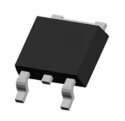
TO252
Applications
• Power Supplies • Inverter
P-Channel MOSFET
Absolute Maximum Ratings
Symbol Parameter Rating -40 ±20 175 -55 to 175 TC=25°C -32
①
Unit
Common Ratings (TC=25°C Unless Otherwise Noted) VDSS VGSS TJ TSTG IS I DP ID Drain-Source Voltage Gate-Source Voltage Maximum Junction Temperature Storage Temperature Range Diode Continuous Forward Current V °C °C A
Mounted on Large Heat Sink 300μs Pulse Drain Current Tested Continuous Drain Current TC=25°C TC=25°C TC=100°C PD RθJC
②
-120
A A
-32 -23 52 26 2.9
Maximum Power Dissipation Thermal Resistance-Junction to Case
TC=25°C TC=100°C
W °C/W
Drain-Source Avalanche Ratings EAS Avalanche Energy, Single Pulsed 144 mJ
Copyright© Ruichips Semiconductor Co., Ltd Rev. A– DEC., 2011
www.ruichips.com
�RU40L10L
Electrical Characteristics
Symbol Static Characteristics BVDSS IDSS VGS(th) IGSS RDS(ON)
③
(TC=25°C Unless Otherwise Noted) RU40L10L Min. Typ. Max.
Parameter
Test Condition
Unit
Drain-Source Breakdown Voltage Zero Gate Voltage Drain Current Gate Threshold Voltage Gate Leakage Current Drain-Source On-state Resistance
VGS=0V, IDS=-250µA VDS= -40V, VGS=0V TJ=85°C VDS=VGS, IDS=-250µA VGS=±20V, VDS=0V VGS= -10V, IDS=-10A VGS= -4.5V, IDS=-8A
-40 -1 -30 -1.0 -1.8 -2.5 ±10 20 30 25 35
V µA V µA mΩ mΩ
Diode Characteristics VSD
trr Qrr
③
Diode Forward Voltage Reverse Recovery Time Reverse Recovery Charge
④
ISD=-1A, VGS=0V ISD=-1A, dlSD/dt=100A/µs
-0.75 36 28
-1
V ns nC Ω pF
Dynamic Characteristics RG Gate Resistance Ciss Coss Crss td(ON) tr td(OFF) tf
VGS=0V,VDS=0V,F=1MHz VGS=0V, VDS= -20V, Frequency=1.0MHz VDD=-20V, RL=0.66Ω, IDS=-30A, VGEN=-10V, RG=6Ω
1.5 2310 250 165 15 23 43 17
Input Capacitance Output Capacitance Reverse Transfer Capacitance Turn-on Delay Time Turn-on Rise Time Turn-off Delay Time Turn-off Fall Time
④
ns
Gate Charge Characteristics Qg Qgs Qgd
Notes:
Total Gate Charge Gate-Source Charge Gate-Drain Charge
Pulse width limited by safe operating area. Limited by TJmax, IAS =24A, VDD =-24V, RG = 50Ω , Starting TJ = 25°C. Pulse test ; Pulse width≤300µs, duty cycle≤2%. Guaranteed by design, not subject to production testing.
45 VDS=-32V, VGS= -10V, IDS=-30A 8 15 nC
Copyright© Ruichips Semiconductor Co., Ltd Rev. A– DEC., 2011
2
www.ruichips.com
�RU40L10L
Typical Characteristics
Power Dissipation Drain Current
Tj - Junction Temperature (°C)
-ID - Drain Current (A)
Tj - Junction Temperature (°C) Safe Operation Area
Ptot - Power (W)
Thermal Transient Impedance
-VDS - Drain-Source Voltage (V)
Copyright© Ruichips Semiconductor Co., Ltd Rev. A– DEC., 2011 3
Normalized Effective Transient
Square Wave Pulse Duration (sec)
www.ruichips.com
-ID - Drain Current (A)
�RU40L10L
Typical Characteristics
Output Characteristics Drain-Source On Resistance
-VDS - Drain-Source Voltage (V)
RDS(ON) - On Resistance (mΩ)
-ID - Drain Current (A)
-ID - Drain Current (A)
Drain-Source On Resistance
Gate Threshold Voltage
-VGS - Gate-Source Voltage (V)
Normalized Threshold Voltage
Tj - Junction Temperature (°C)
4
Copyright© Ruichips Semiconductor Co., Ltd Rev. A– DEC., 2011
RDS(ON) - On - Resistance (m)
www.ruichips.com
�RU40L10L
Typical Characteristics
Drain-Source On Resistance Source-Drain Diode Forward
Normalized On Resistance
Tj - Junction Temperature (°C)
-IS - Source Current (A)
-VSD - Source-Drain Voltage (V) Capacitance
Gate Charge
-VDS - Drain-Source Voltage (V)
-VGS - Gate-Source Voltage (V)
C - Capacitance (pF)
QG - Gate Charge (nC)
Copyright© Ruichips Semiconductor Co., Ltd Rev. A– DEC., 2011
5
www.ruichips.com
�RU40L10L
Avalanche Test Circuit and Waveforms
Switching Time Test Circuit and Waveforms
Copyright© Ruichips Semiconductor Co., Ltd Rev. A– DEC., 2011
6
www.ruichips.com
�RU40L10L
Ordering and Marking Information
Device RU40L10L Marking RU40L10L Package TO-252 Packaging Tape&Reel Quantity 2500 Reel Size 13’’ Tape width 16mm
Copyright© Ruichips Semiconductor Co., Ltd Rev. A– DEC., 2011
7
www.ruichips.com
�RU40L10L
Package Information
TO252-2L
SYMBOL A A1 b C D D1 D2 E e
MM MIN 2.200 0.000 0.660 0.460 6.500 5.100 6.000 2.186 MAX 2.400 0.127 0.860 0.580 6.700 5.460 6.200 2.386 MIN
INCH MAX 0.094 0.005 0.034 0.023 0.264 0.215 0.244 0.094 SYMBOL L L1 L2 L3 L4 Φ θ h V MIN 9.800 1.400 0.600 1.100 0° 0.000 0.087 0.000 0.026 0.018 0.256 0.201 0.236 0.086
MM MAX 10.400 1.700 1.000 1.300 8° 0.300
INCH MIN 0.386 0.055 0.024 0.043 0° 0.000 MAX 0.409 0.067 0.039 0.051 8° 0.012
2.900 REF. 1.600 REF.
0.114 REF. 0.063REF.
4.830 REF.
0.190 REF.
5.350 REF.
0.211 REF.
ALL DIMENSIONS REFER TO JEDEC STANDARD DO NOT INCLUDE MOLD FLASH OR PROTRUSIONS
Copyright© Ruichips Semiconductor Co., Ltd Rev. A– DEC., 2011
8
www.ruichips.com
�RU40L10L
Customer Service
Worldwide Sales and Service: Sales@ruichips.com Technical Support: Technical@ruichips.com Investor Relations Contacts: Investor@ruichips.com Marcom Contact: Marcom@ruichips.com Editorial Contact: Editorial@ruichips.com HR Contact: HR@ruichips.com Legal Contact:
Legal@ruichips.com Shen Zhen RUICHIPS Semiconductor CO., LTD
Room 501, the 5floor An Tong Industrial Building, NO.207 Mei Hua Road Fu Tian Area Shen Zhen City, CHINA TEL: (86-755) 8311-5334 FAX: (86-755) 8311-4278 E-mail: Sales-SZ@ruichips.com
Copyright© Ruichips Semiconductor Co., Ltd Rev. A– DEC., 2011
9
www.ruichips.com
�