Metal Composite Power Inductor (wire wound)
Specification Sheet
CIGW160808XMR47MLC (1608 / EIA 0603)
APPLICATION
Smart phones, Tablet, Wearable devices, Power converter modules, etc.
FEATURES
RECOMMENDED LAND PATTERN
Small power inductor for mobile devices
Low DCR structure and high efficiency inductor for power circuits.
Monolithic structure for high reliability
Free of all RoHS-regulated substances
Halogen free
TYPE
A
B
C
Unit : mm
1608
0.8
0.5
0.9
DIMENSION
TYPE
1608
L
1.6±0.2
Dimension [mm]
W
T
0.8±0.2
0.7±0.1
D
0.35±0.15
DESCRIPTION
Part no.
Size
[inch/mm]
Thickness
[mm] (max)
Inductance
[uH]
Inductance
tolerance
(%)
CIGW160808XMR47MLC
0603/1608
0.8
0.47
±20
DC Resistance [mΩ]
Rated DC Current *1 [A]
Rated DC Current *2 [A]
Max.
Typ.
Max.
Typ.
Max.
Typ.
43
37
2.7
3
3
3.3
* Inductance : Measured with a LCR meter 4991A(Agilent) or equivalent (Test Freq. 1MHz, Level 0.1V)
* DC Resistance : Measured with a Resistance HI-TESTER 3541(HIOKI) or equivalent
* Maximum allowable DC current : Value defined when DC current flows and the nominal value of inductance has decreased by 30% or
when current flows and temperature has risen to 40℃ whichever is smaller. (Reference: ambient temperature is 25℃±10)
(Isat) : Allowable current in DC saturation : The DC saturation allowable current value is specified when the decrease of
the nominal inductance value at 30% (Reference: ambient temperature is 25℃±10)
(Irms) : Allowable current of temperature rise : The temperature rise allowable current value is specified when temperature of
the inductor is raised 40℃ by DC current. (Reference: ambient temperature is 25℃±10)
* Absolute maximum voltage : Rated Voltage 20V.
* Operating temperature range : -–40 to +125°C (Including self-temperature rise)
PRODUCT IDENTIFICATION
CIG
(1)
W
(2)
1608
(3)
08
(4)
(1) Power Inductor
(3) Dimension (1608: 1.6mm × 0.8mm )
(5) Remark (Characterization Code)
(7) Tolerance(M:±20%)
(8) Internal Code
(9) Packaging (C:paper tape, E:embossed tape)
XM
(5)
R47
(6)
L
(8)
(2) Type
(T: Metal Composite Thin Film Type)
(4) Thickness (08: 0.8mm)
(6) Inductance(R47: 0.47 uH)
RECOMMENDED SOLDERING CONDITION
REFLOW SOLDERING
M
(7)
FLOW SOLDERING
PACKAGING
Packaging Style
Quantity(pcs/reel)
Card Board Taping
4000 pcs
C
(9)
�Reliability Test
Item
Specified Value
Test Condition
More than 90% of terminal electrode should be
soldered newly.
After being dipped in flux for 4±1 seconds, and preheated at
150∼180℃ for 2∼3 min, the specimen shall be immersed in
solder at 245±5℃ for 4±1 seconds.
Resistance to Soldering
No mechanical damage.
Remaining terminal Electrode: 75% min.
Inductance change to be within ±20% to the initial.
After being dipped in flux for 4±1 seconds, and preheated at
150∼180℃ for 2∼3 min, the specimen shall be immersed in
solder at 260±5℃ for 10 ±0.5 seconds.
Thermal Shock
(Temperature Cycle test)
No mechanical damage
Inductance change to be within ±20% to the initial.
Repeat 100 cycles under the following conditions.
-40±3℃ for 30 min → 85±3℃ for 30 min
High Temp. Humidity
Resistance Test
No mechanical damage
Inductance change to be within ±20% to the initial
85±2℃, 85%RH, for 500±12 hours.
Measure the test items after leaving at normal temperature and
humidity for 24 hours.
Low Temperature Test
No mechanical damage
Inductance change to be within ±20% to the initial.
Solder the sample on PCB. Exposure
at -55±2℃ for 500±12 hours.
Measure the test items after leaving at normal temperature and
humidity for 24hours.
High Temperature Test
No mechanical damage
Inductance change to be within ±20% to the initial.
Solder the sample on PCB. Exposure at 125±2℃ for 500±12
hours.
Measure the test items after leaving at normal temperature and
humidity for 24hours.
High Temp. Humidity Resistance
Loading Test
No mechanical damage
Inductance change to be within ±20% to the initial
85±2℃, 85%RH, Rated Current for 500±12 hours.
Measure the test items after leaving at normal temperature and
humidity for 24 hours.
High Temperature Loading Test
No mechanical damage
Inductance change to be within ±20% to the initial
85±2℃, Rated Current for 500±12 hours.
Measure the test items after leaving at normal temperature and
humidity for 24 hours.
Reflow Test
No mechanical damage
Inductance change to be within ±20% to the initial
Peak 260±5℃, 3 times
Vibration Test
No mechanical damage
Inductance change to be within ±20% to the initial.
Solder the sample on PCB. Vibrate as apply 10~55Hz, 1.5mm
amplitude for 2 hours in each of three(X,Y,Z) axis (total 6 hours).
No mechanical damage
Bending Limit; 2mm
Test Speed; 1.0mm/sec.
Keep the test board at the limit point in 5 sec.
PCB thickness : 1.6mm
Solderability
Bending Test
No indication of peeling shall occur on the terminal
electrode.
W(kgf)
TIME(sec)
0.5
10±1
Terminal Adhesion Test
Drop Test
No mechanical damage
Inductance change to be within ±20% to the initial.
Random Free Fall test on concrete plate.
1 meter, 10 drops
�Metal Composite Power Inductor (wire wound)
Data Sheet
1. Model : CIGW160808XMR47MLC
2. Description
Size
[inch/mm]
Thickness
[mm] (max)
Inductance
[uH]
Inductance
tolerance
(%)
0603/1608
0.8
0.47
±20
Part no.
CIGW160808XMR47MLC
DC Resistance [mΩ]
Rated DC Current *1 [A]
Rated DC Current *2 [A]
Max.
Typ.
Max.
Typ.
Max.
Typ.
43
37
2.7
3
3
3.3
* Inductance : Measured with a LCR meter 4991A(Agilent) or equivalent (Test Freq. 1MHz, Level 0.1V)
* DC Resistance : Measured with a Resistance HI-TESTER 3541(HIOKI) or equivalent
* Maximum allowable DC current : Value defined when DC current flows and the nominal value of inductance has decreased by 30% or
when current flows and temperature has risen to 40℃ whichever is smaller. (Reference: ambient temperature is 25℃±10)
(Isat) : Allowable current in DC saturation : The DC saturation allowable current value is specified when the decrease of
the nominal inductance value at 30% (Reference: ambient temperature is 25℃±10)
(Irms) : Allowable current of temperature rise : The temperature rise allowable current value is specified when temperature of
the inductor is raised 40℃ by DC current. (Reference: ambient temperature is 25℃±10)
* Absolute maximum voltage : Rated Voltage 20V.
* Operating temperature range : -–40 to +125°C (Including self-temperature rise)
3. Characteristics data
1) Frequency characteristics (Ls)
2) Frequency characteristics (Q)
Agilent E4294A +E4991A , 1MHz to 1,000MHz
Agilent E4294A +E4991A , 1MHz to 1,000MHz
45
0.8
40
0.6
30
0.2
Q
Inductance [uH]
35
0.4
25
20
0
15
-0.2
10
-0.4
5
-0.6
0
1
10
100
1000
1
10
Frequency [MHz]
0.60
Inductance [uH]
0.55
0.50
0.45
0.40
0.35
0.30
0.25
0.20
1
DC Current [A]
1000
4)Temperature characteristics (Typ.)
Temperature rate of change [℃]
3) DC Bias characteristics (Typ.)
0
100
Frequency [MHz]
2
3
50
40
30
20
10
0
-10
0.0
1.0
2.0
DC Current [A]
Any data in this sheet are subject to change, modify or discontinue without notice
The data sheets include the typical data for design reference only. If there is any question
regarding the data sheets, please contact our sales personnel or application engineers
3.0
�
很抱歉,暂时无法提供与“CIGW160808XMR47MLC”相匹配的价格&库存,您可以联系我们找货
免费人工找货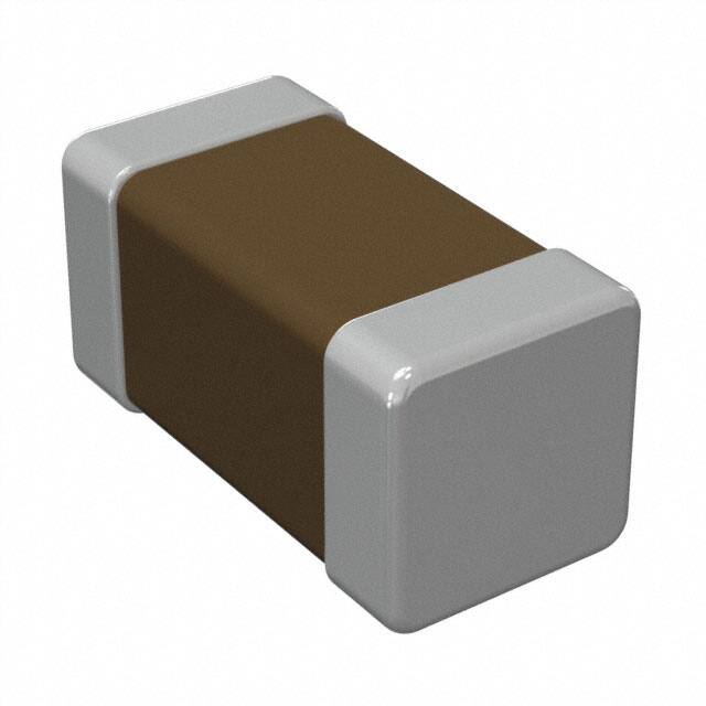


 工商网监
湘ICP备2023018690号
工商网监
湘ICP备2023018690号
