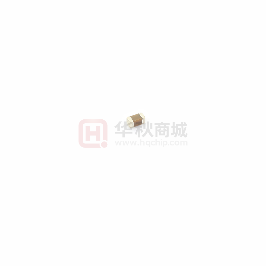
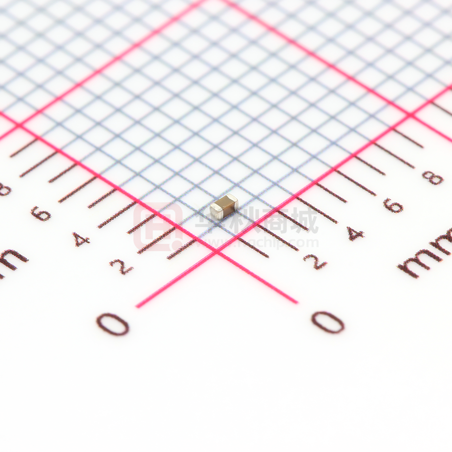
此商品编号的参数规格是: CL05B333KO5NNNC/0402
33nF, 0402封装
CL 10
1
2
A 106 M
P
8
N
N
N
C
3
6
7
8
9
10
11
4
5
1. SERIES CODE
CL = Multi layer Ceramic Capacitors
inch(㎜)
2. SIZE CODE
02 = 01005(0402)
03 = 0201(0603)
05 = 0402(1005)
10 = 0603(1608)
21 = 0805(2012)
31 = 1206(3216)
32 = 1210(3225)
42 = 1808(4520)
43 = 1812(4532)
55 = 2220(5750)
★
3. DIELECTRIC CODE
ClassⅠ
ClassⅡ
C = C0G
A = X5R F = Y5V
B = X7R X = X6S
Y = X7S Z = X7T
★★
4. CAPACITANCE CODE
Capacitance expressed in ㎊. 2 significant digits plus number of zeros.
example) 106 =10Ⱌ106 =10000000㎊
For Values ⾘ 10 ㎊, Letter R denotes decimal point
example) 1R5 =1.5㎊
5. TOLERANCE CODE
B =Ⰽ0.1㎊
C =Ⰽ0.25 ㎊
D =Ⰽ0.5 ㎊
F = Ⰽ1㎊, Ⰽ1%�
G= Ⰽ2%
J =Ⰽ5%
K =Ⰽ10%
M =Ⰽ20%
Z = �80/�20%
*For Values ≤ 10㎊, F =Ⰽ1㎊
Values ⾘10㎊, F =Ⰽ1%
6. RATED VOLTAGE CODE
R = 4V
Q = 6.3V
P = 10V
O = 16V
A = 25V
L = 35V
B = 50V
C = 100V
D = 200V
E = 250V
F = 350V
G = 500V
H = 630V
I = 1000V
J = 2000V
K = 3000V
★★★
7. THICKNESS CODE
2 = 0.20 ㎜
3 = 0.30㎜
5 = 0.50㎜
8 = 0.80㎜
9 = 0.90㎜
A = 0.65㎜ F = 1.25 ㎜
C = 0.85㎜ H = 1.60 ㎜
D = 1.00㎜ I = 2.00㎜
E = 1.10㎜ J = 2.50㎜
L = 3.20 ㎜
M = 1.15 ㎜
P = 1.15 ㎜
Q = 1.25 ㎜
S = 1.35 ㎜
U = 1.80⽆
V = 2.50 ㎜
Y = 1.25 ㎜
8. INNER ELECTRODE/TERMINATION/PLATING CODE
A = Normal Product Pd / Ag / Ni barrier / Sn 100%
N = Normal Product Ni / Cu / Ni barrier / Sn 100%
G = Normal Product Cu / Cu / Ni barrier / Sn 100%
L = Low profile Ni / Cu / Ni barrier / Sn 100%
S = Nomal Product Ni / Cu / Soft termination / Ni barrier / Sn100%
9. PRODUCT CODE
N = Normal
A = Array(4-element)
B = Array(4-element)
L = LICC
J = SLIC
10. CONTROL CODE
*Size tolerance
Size
01005(0402) 0201(0603) 0402(1005) 0603(1608) 0805(2012) 1206(3216)
Code
Ⰽ0.03
Ⰽ0.05
Ⰽ0.07
Ⰽ0.07
Ⰽ0.30
S
Ⰽ0.05
Ⰽ0.07
Ⰽ0.10
Ⰽ0.15
Ⰽ0.15
Q
Ⰽ0.07
Ⰽ0.09
Ⰽ0.15
Ⰽ0.20
Ⰽ0.20
R
Ⰽ0.09
Ⰽ0.20
Ⰽ0.25
Ⰽ0.30
U
Ⰽ0.40
Ⰽ0.30
Z
9
Ⰽ0.30
N= Reserved for future use
11. PACKAGING CODE
B = Bulk
O = Cardboard Tape, 10”Reel
E = Embossed Type, 7”Reel
P = Bulk Case
D = Cardboard Tape, 13”Reel (10,000ea)
G = Embossed Type, 7”Reel (3,000ea)
C= Cardboard Tape, 7”Reel
L = Cardboard Tape, 13”Reel (15,000ea)
F = Embossed Type, 13”Reel
H = Cardboard Tape, 7”Reel (15,000ea)
S = Embossed Type, 10”Reel
8 = Cardboard Tape, 7”Reel
Z = Cardboard Type, 7”Reel (Chip aligned for horizontal SMT)
Y = Cardboard Type, 7”Reel (Chip aligned for vertical SMT)
�Class I (Temperature Compensation)
Symbol
EIA Code
Operation Temperature Range( ℃)
Temperature Coefficient Range(ppm/℃)
C
C0G
�55 _��125
0 Ⰽ30
★
Class ll (High Dielectric Constant)
Symbol
EIA Code
Operation Temperature Range( ℃)
Capacitance Change(△℃%)
A
B
X
F
Y
Z
X5R
X7R
X6S
Y5V
X7S
X7T
�55 _�� 85
�55 _��125
�55 _��105
�30 _�� 85
�55 _��125
�55 _��125
Ⰽ15
Ⰽ15
Ⰽ 22
�82 _��22
Ⰽ22
�33 _��22
★★
Series
TC
E-3
Y5V
X5R
X7R
X6S
X7S
X7T
C0G
E-6
E-12
Capacitance Step
1.0
1.0
1.5
1.2
4.7
2.2
1.0
1.5
2.2
1.8
2.2
3.3
2.7
3.3
4.7
3.9
4.7
6.8
5.6
6.8
8.2
★★★
Size
Code
Thickness(mm)
01005(0402)
0201(0603)
2
3
3
5
5
8
A
C
C
M
F
Q
Y
C
C
E
E
P
M
F
H
0.20
0.30
0.30
0.50
0.50
0.80
0.65
0.85
0.85
1.15
1.25
1.25
1.25
0.85
0.85
1.10
1.10
1.15
1.15
1.25
1.60
0402(1005)
0603(1608)
0805(2012)
1206(3216)
Spec(mm)
Ⰽ0.02
Ⰽ0.03
Ⰽ0.03*
Ⰽ0.05
� 0.0/�0.1*
Ⰽ0.10
Ⰽ0.10
Ⰽ0.10
Ⰽ0.10*
Ⰽ0.10
Ⰽ0.10
Ⰽ0.15
Ⰽ0.20
Ⰽ0.15
Ⰽ0.10*
Ⰽ0.15
Ⰽ0.10*
Ⰽ0.10*
Ⰽ0.15
Ⰽ0.15
Ⰽ0.20
Size
1210(3225)
1808(4520)
1812(4532)
2220(5750)
Code
C
9
F
S
H
U
I
J
V
F
H
I
F
H
I
J
L
H
I
J
L
Thickness(mm)
0.85
0.90
1.25
1.35
1.60
1.80
2.00
2.50
2.50
1.25
1.60
2.00
1.25
1.60
2.00
2.50
3.20
1.60
2.00
2.50
3.00
Spec(mm)
Ⰽ0.10*
Ⰽ0.10*
Ⰽ0.20
Ⰽ0.15
Ⰽ0.20
Ⰽ0.20*
Ⰽ0.20
Ⰽ0.20
Ⰽ0.30
Ⰽ0.20
Ⰽ0.20
Ⰽ0.20
Ⰽ0.20
Ⰽ0.20
Ⰽ0.20
Ⰽ0.20
Ⰽ0.30
Ⰽ0.20
Ⰽ0.20
Ⰽ0.20
Ⰽ0.30
�Feature
t Wide selection of size : from 0402 to 2220
t Highly reliable tolerance and high speed automatic chip placement on PCBs
t Wide capacitance range
t Wide temperature compensation and voltage range
: from C0G to Y5V and from 6.3V to 50V
t Highly reliable performance
t Highly resistant termination metal
t Tape & reel for surface mount assembly
Application
t HHP, DSC, DVC, LCD, TV, Memory Module, PDA, Game Machine
t Tuner (Product code C is suitable.)
t Desktop PC, Note PC, HHP, DC-DC Converter, DSC
Structure and Dimensions
L
W
T
BW
Size Code
EIA Code
05
0402
10
0603
21
0805
31
1206
32
1210
42
1808
43
1812
55
2220
Dimension(mm)
L
W
T
Thickness Code
BW
1.00Ⰽ0.05
1.60Ⰽ0.10
1.60Ⰽ0.10
2.00Ⰽ0.10
2.00Ⰽ0.10
2.00Ⰽ0.10
2.00Ⰽ0.15
2.00Ⰽ0.20
3.20Ⰽ0.20
3.20Ⰽ0.15
3.20Ⰽ0.20
3.20Ⰽ0.20
3.20Ⰽ0.15
3.20Ⰽ0.20
3.20Ⰽ0.30
3.20Ⰽ0.30
3.20Ⰽ0.30
3.20Ⰽ0.30
3.20Ⰽ0.30
3.20Ⰽ0.30
3.20Ⰽ0.40
4.50Ⰽ0.40
4.50Ⰽ0.40
4.50Ⰽ0.40
4.50Ⰽ0.40
4.50Ⰽ0.40
4.50Ⰽ0.40
5.70Ⰽ0.40
5.70Ⰽ0.40
0.50Ⰽ0.05
0.80Ⰽ0.10
0.80Ⰽ0.10
1.25Ⰽ0.10
1.25Ⰽ0.10
1.25Ⰽ0.10
1.25Ⰽ0.15
1.25Ⰽ0.20
1.60Ⰽ0.20
1.60Ⰽ0.15
1.60Ⰽ0.20
1.60Ⰽ0.20
1.60Ⰽ0.15
1.60Ⰽ0.20
2.50Ⰽ0.20
2.50Ⰽ0.20
2.50Ⰽ0.20
2.50Ⰽ0.20
2.50Ⰽ0.20
2.50Ⰽ0.20
2.50Ⰽ0.30
2.00Ⰽ0.20
2.00Ⰽ0.20
2.00Ⰽ0.20
3.20Ⰽ0.30
3.20Ⰽ0.30
3.20Ⰽ0.30
5.00Ⰽ0.40
5.00Ⰽ0.40
0.50Ⰽ0.05
0.50�0.0/�0.1(*)
0.80Ⰽ0.10
0.85Ⰽ0.10
1.15Ⰽ0.10
1.25Ⰽ0.10
1.25Ⰽ0.15
1.25Ⰽ0.20
0.60Ⰽ0.10(*)
0.85Ⰽ0.15
0.85Ⰽ0.10(*)
1.15Ⰽ0.10(*)
1.25Ⰽ0.15
1.60Ⰽ0.20
0.85Ⰽ0.10(*)
0.90Ⰽ0.10(*)
1.60Ⰽ0.20
1.80Ⰽ0.20(*)
2.00Ⰽ0.20
2.50Ⰽ0.20
2.50Ⰽ0.30
1.25Ⰽ0.20
1.40Ⰽ0.20
2.00Ⰽ0.20
1.25Ⰽ0.20
2.50Ⰽ0.20
3.20Ⰽ0.30
2.50Ⰽ0.20
3.20Ⰽ0.30
5
5
8
C
M
F
Q
0.25Ⰽ0.10
Y
6
C
C
P
F
H
C
9
H
U
I
J
V
F
G
I
F
J
L
J
L
0.30Ⰽ0.20
0.5�0.2/�0.3
0.50Ⰽ0.30
0.60Ⰽ0.30
0.80Ⰽ0.30
0.80Ⰽ0.30
1.00Ⰽ0.30
�Product Lineup (Standard & High Capacitors-X7R, X7S)
Part Number
1
2
3
4
5
6
7
8
9
10
11
12
13
14
15
16
17
18
19
20
21
22
23
24
25
26
27
28
29
30
31
32
33
34
35
1
37
38
39
40
41
42
43
44
45
46
47
48
49
50
51
52
CL05B151KB5NNN
CL05B181KB5NNN
CL05B221KB5NNN
CL05B271KB5NNN
CL05B331KB5NNN
CL05B391KB5NNN
CL05B471KB5NNN
CL05B561KB5NNN
CL05B681KB5NNN
CL05B102KB5NNN
CL05B122KB5NNN
CL05B152KB5NNN
CL05B182KB5NNN
CL05B222KB5NNN
CL05B272KB5NNN
CL05B332KB5NNN
CL05B472KB5NNN
CL05B562KB5NNN
CL05B682KB5NNN
CL05B822KB5NNN
CL05B103KB5NNN
CL05B123KA5NNN
CL05B153KA5NNN
CL05B223KA5NNN
CL05B273KO5NNN
CL05B333KO5NNN
CL05B393KO5NNN
CL05B473KO5NNN
CL05B563KO5NNN
CL05B683KO5NNN
CL05B823KO5NNN
CL05B104KO5NNN
CL05B224KO5NNN
CL05B474KP5NNN
CL05B105KQ5NQN
CL05Y474KP5NNN
CL10B101KB8NNN
CL10B121KB8NNN
CL10B151KB8NNN
CL10B181KB8NNN
CL10B201KB8NNN
CL10B221KB8NNN
CL10B271KB8NNN
CL10B331KB8NNN
CL10B391KB8NNN
CL10B471KB8NNN
CL10B561KB8NNN
CL10B681KB8NNN
CL10B751KB8NNN
CL10B821KB8NNN
CL10B102KB8NNN
CL10B122KB8NNN
Size L x W
(mm)
1.00Ⱌ0.50
1.00Ⱌ0.50
1.60Ⱌ0.80
Capacitance
Rated
Voltage
(Vdc)
Capacitance
Tolerance
Thickness
Max.(mm)
150㎊
180㎊
220㎊
270㎊
330㎊
390㎋
470㎊
560㎊
680㎊
1㎋
1.2㎋
1.5㎋
1.8㎋
2.2㎋
2.7㎋
3.3㎋
4.7㎋
5.6㎋
6.8㎋
8.2㎋
10㎋
12㎋
15㎋
22㎋
27㎋
33㎋
39㎋
47㎋
56㎋
68㎋
82㎋
100㎋
220㎋
470㎋
1㎌
470㎋
100㎊
120㎊
150㎊
180㎊
200㎊
220㎊
270㎊
330㎊
390㎊
470㎊
560㎊
680㎊
750㎊
820㎊
1㎋
1.2㎋
50
50
50
50
50
50
50
50
50
50
50
50
50
50
50
50
50
50
50
50
50
25
25
25
16
16
16
16
16
16
16
16
16
10
6.3
10
50
50
50
50
50
50
50
50
50
50
50
50
50
50
50
50
Ⰽ10%
Ⰽ10%
Ⰽ10%
Ⰽ10%
Ⰽ10%
Ⰽ10%
Ⰽ10%
Ⰽ10%
Ⰽ10%
Ⰽ10%
Ⰽ10%
Ⰽ10%
Ⰽ10%
Ⰽ10%
Ⰽ10%
Ⰽ10%
Ⰽ10%
Ⰽ10%
Ⰽ10%
Ⰽ10%
Ⰽ10%
Ⰽ10%
Ⰽ10%
Ⰽ10%
Ⰽ10%
Ⰽ10%
Ⰽ10%
Ⰽ10%
Ⰽ10%
Ⰽ10%
Ⰽ10%
Ⰽ10%
Ⰽ10%
Ⰽ10%
Ⰽ10%
Ⰽ10%
Ⰽ10%
Ⰽ10%
Ⰽ10%
Ⰽ10%
Ⰽ10%
Ⰽ10%
Ⰽ10%
Ⰽ10%
Ⰽ10%
Ⰽ10%
Ⰽ10%
Ⰽ10%
Ⰽ10%
Ⰽ10%
Ⰽ10%
Ⰽ10%
0.55
0.55
0.55
0.55
0.55
0.55
0.55
0.55
0.55
0.55
0.55
0.55
0.55
0.55
0.55
0.55
0.55
0.55
0.55
0.55
0.55
0.55
0.55
0.55
0.55
0.55
0.55
0.55
0.55
0.55
0.55
0.55
0.55
0.55
0.60
0.55
0.90
0.90
0.90
0.90
0.90
0.90
0.90
0.90
0.90
0.90
0.90
0.90
0.90
0.90
0.90
0.90
�No
Item
1
Appearance
2
Insulation Resistance
Performance
Test Condition
No abnormal exterior appearance
Visual Inspection throughMicroscope (x10)
10,000㏁ min. or 500 ㏁ ・ ㎌ min.(or*100㏁ ň㎌)
product whichever is smaller
(Rated voltageⴍ16V:10,000㏁ min. or100㏁ ň㎌
min. product whichever is smaller)
Apply the rated voltage for 60~120 sec.
Ratedvoltage⾚500V: InsulationResistance shall be
measured with 500Ⰽ50Vdc
Apply the specified voltage* for 1~5 sec.
Charge / Discharge current limit: 50mA max.
*CLASSⅠ(Rated Voltage⾘100V) : 300% of the rated Voltage
CLASSⅡ(Rated Voltage⾘100V) : 250% of the rated Voltage
3
Withstanding Voltage
CLASSⅠ
No dielectric breakdown or mechanical breakdown
Within the specified tolerance
4
Capaci
tance
CLASSⅡ
Within the specified tolerance
In the case of Vr ⴎ100V products, following condition should
be applied.
100VⴍRated Voltage⾘500V : 200% of the rated Voltage
500VⴍRated Voltage⾘1000V :150% of the rated Voltage
Rated Voltageⴎ1000V :120% of the rated Voltage
Capacitance
ⴍ1,000㎊
⾚1,000㎊
Capacitance
ⴍ10㎌
⾚10㎌
*
Frequency
1MHzⰍ10%
1KHzⰍ10%
Frequency
1KHzⰍ10%
120HzⰍ20%
1KHzⰍ10%
Voltage
0.5 ~ 5 Vrms
Voltage
1.0Ⰽ0.2Vrms
0.5Ⰽ0.1Vrms
0.5Ⰽ0.1Vrms
* A capacitor prior to measuring the capacitance is heat
treated at 150℃�0/�10℃ and maintained in ambient
air for 24Ⰽ2 hours.
Q
CLASSⅠ
Capacitance ⴎ 30㎊: Q ⴎ1,000
⾘ 30㎊: Qⴎ400 �20ⰜC
(C : Capacitance)
1. Characteristic : A(X5R)
Rated Voltage
Spec
50V /35V
0.025 max / 0.05 max*
0.025 max /
25V
0.05 max* / 0.10 max*
0.035 max /
16V
0.05 max* / 0.10 max*
ⴍ10V
0.05 max /0.10 max*
5
TanѰ
CLASSⅡ
Capacitance
ⴍ1,000㎊
⾚1,000㎊
Capacitance
ⴍ10㎌
⾚10㎌
*
Frequency
1MHzⰍ10%
1KHzⰍ10%
Frequency
1KHzⰍ10%
120HzⰍ20%
1KHzⰍ10%
Voltage
0.5 ~ 5 Vrms
Voltage
1.0Ⰽ0.2Vrms
0.5Ⰽ0.1Vrms
0.5Ⰽ0.1Vrms
2. Characteristic : B(X7R), X(X6S), Y(X7S)
Rated Voltage
Spec
0.025 max /
50Vⴎ/ 35V / 25V
0.05 max* / 0.10 max*
16V
0.035 max / 0.10 max*
0.05 max /0.10 max*
ⴍ10V
3. Characteristic : F(Y5V)
Rated Voltage
50V / 35V / 25V
16V
10V
ⴍ6.3V
Spec
0.05 max /
0.07 max* / 0.09 max*
0.07 max /
0.09 max* / 0.125 max*
0.125 max /0.16 max*
0.16 max
You can check the specification at the web site or contact sales
people for each product with mark*
�No
Item
Performance
Test Condition
Capacitance shall be measured by the steps shown in the following table.
6
Temperature
Characteristics
of Capacitance
CLASSⅠ
CLASSⅡ
Characteristic
C
Temp.Coefficient(PPM/℃)
0Ⰽ30
Characteristic
Capacitance Change(%)
with No bias
A(X5R)/ B(X7R)
X(X6S), Y(X7S)
Z(X7T)
F(Y5V)
Ⰽ15%
Ⰽ22%
�22%~�33%
�22%~�82%
Step
1
2
3
4
5
Temperature (℃ )
25Ⰽ2
Min. Operating Temp. Ⰽ2
25Ⰽ2
Max. Operating Temp. Ⰽ2
25Ⰽ2
(1) CLASSм
Temperature Coefficient shall be calculated from the formula as below
C2�C1
Temp. Coefficient =
ţ106 [ppm/℃]
C1ⰜⶹT
C1: Capacitance at step 3
C2: Capacitance at 125℃
ⶹT: 100℃ (=125℃ �25℃ )
(2) CLASSн
Capacitance Change shall be calculated from the formula as below
C2�C1
ⶹC=
Ⱌ100(%)
C1
C1: Capacitance at step 3
C2: Capacitance at step 2 or 4
Apply 500g.f* pressure for 10Ⰽ1 sec. *200g.f for 0201
*100g.f for 01005
7
Adhesive Strength of
Termination
Appearance
8
Bending
Strength
Capacitance
No indication of peeling shall occur on the terminal
electrode
No indication of peeling shall occur
Characteristic
Capacitance Change
CLASSⅠ
Ⰽ5% or Ⰽ 0.5 pF
whichever is larger
A(X5R), B(X7R),
X(X6S), Y(X7S) Ⰽ12.5%
CLASSⅡ
Z(X7T)
F(Y5V)
Ⰽ30%
More than 75% of the terminal surface is to be soldered
newly, so metal part does not come out or dissolve
9
Solderability
Appearance
Capacitance
Resistance
10 to Soldering
Heat
No mechanical damage shall occur
Characteristic
Capacitance Change
CLASSⅠ
Ⰽ2.5% or Ⰽ 0.25 pF
whichever is larger
A(X5R), B(X7R),
CLASSⅡ X(X6S), Y(X7S) Ⰽ7.5%
Z(X7T)
F(Y5V)
Q
(CLASSⅠ�
TanѰ
(CLASSⅡ)
Insulation
resistance
Withstanding
voltage
Ⰽ20%
Within the specified initial value
Within the specified initial value
Within the specified initial value
Within the specified initial value
500g.f
ҟBending Limit: 1mm ҟTest Speed: 1.0mm/sec.
ҟKeep the test board at the limit point in 5 sec.
ҟThen Measure Capacitance
20
50
45Ⰽ1
Solder
Solder Temp.
Flux
Dip time
Pre-heating
R=230
45Ⰽ1
Bending limit
Sn�3Ag�0.5Cu
245Ⰽ5℃
RMA Type
3Ⰽ0.3 sec.
at 80~120℃ for 10~30 sec.
Solder temperature: 270Ⰽ5℃ DIP TIME:10Ⰽ1 sec.
Each termination shall be fully immersed and preheated as below:
Step
Temperature(℃)
Time (sec.)
1
2
80~100
150~180
60
60
Leave the capacitor in ambient condition for specified time* before
measurement
*24 Ⰽ 2 hours(CLASSⅠ�
24 Ⰽ 2 hours(CLASSⅡ)
�No
Item
Appearance
Performance
No mechanical damage shall occur
Characteristic
CLASSⅠ
A(X5R), B(X7R)
Capacitance
11
X(X6S), Y(X7S)
CLASSⅡ Z(X7T)
Vibration
Test
F(Y5V)
Q
(CLASSм)
TanѰ
(CLASSⅡ)
Insulation
resistance
Appearance
Capacitance Change
Ⰽ2.5% or Ⰽ 0.25 pF
whichever is larger
Ⰽ5%
Ⰽ20%
Within the specified initial value
Within the specified initial value
No mechanical damage shall occur
CLASSⅠ
Capacitance Change
Ⰽ7.5% or Ⰽ 0.75pF
whichever is larger
500㏁ min. or 25㏁・㎌ min.
product whichever is smaller / 12.5㏁ ・㎌ or over*
No mechanical damage shall occur
Characteristic
CLASSⅠ
Capacitance Change
Ⰽ3% or Ⰽ 0.3 pF
whichever is larger
A(X5R), B(X7R),
X(X6S), Y(X7S)
Ⰽ12.5%
Z(X7T)
Ⰽ30%
F(Y5V)
Capacitanceⴎ30㎊ : Qⴎ350
Q
10ⴍCapacitance⾘30㎊: Qⴎ275�2.5ⰜC
(CLASSⅠ� Capacitance⾘10㎊ : Qⴎ200+10ţC (C: Capacitance)
1.Capacitance : A(X5R)
0.05 max / 0.075 max* (35V / 50V)
0.05 max / 0.075 max* / 0.125 max*(16V / 25V)
0.075 max / 0.125 max* (Ŧ10V)
2.Capacitance : B(X7R), X(X6S)
0.05 max / 0.125 max* (16V / 25V / 35V / 50Vŧ)
TanѰ
0.075 max / 0.125 max* (Ŧ10V)
(CLASSⅡ)
3.Capacitance : F(Y5V)
0.09 max (50V)
0.09 max / 0.125 max* (25V / 35V)
0.09 max / 0.125 max* / 0.16 max* (16V)
0.16 max / 0.195 max* (10V)
0.195 max (4V / 6.3V)
Capacitance
CLASSⅡ
High Temperature Resistance
Applied Voltage: rated voltage
Temperature: 40Ⰽ2℃
Humidity: 90~95% RH
Duration Time: 500�12/�0 Hr.
Charge/Discharge Current: 50㎃ max.
A(X5R), B(X7R),
X(X6S), Y(X7S) Ⰽ12.5%
CLASSⅡ Z(X7T)
Perform the initial measurement according to Note1.
F(Y5V)
Ⰽ30%
Perform the final measurement according to Note2.
Capacitanceŧ30㎊: Qⴎ200
Q
⾘30㎊: Qⴎ100+10/3ⰜC(C: Capacitance)
(CLASSⅠ�
1.Capacitance: A(X5R)
0.05 max / 0.075 max* (35V / 50V)
0.05 max / 0.075 max* / 0.125 max*(16V / 25V)
0.075 max / 0.125 max* (ⴍ10V)
2.Capacitance: B(X7R), X(X6S)
TanѰ
0.05 max / 0.125 max* (16V / 25V / 35V / 50Vⴎ)
(CLASSⅡ)
0.075 max / 0.125 max* (ⴍ10V)
3.Capacitance: F(Y5V)
0.09 max (50V)
0.09 max / 0.125 max* (25V / 35V)
This test is only applied to Vrⴍ500V products.
0.09 max / 0.125 max* / 0.16 max* (16V)
You can check the specification at the web site or contact sales people
0.16 max / 0.195 max* (10V)
0.195 max (4V / 6.3V)
for each product with mark*
Insulation
resistance
Appearance
13
Repeat this for 2hours each in 3 mutually perpendicular directions.
Ⰽ10%
Capacitance
Moisture
Resistance
The capacitor shall be subjected to a harmonic motion having a total
amplitude of 1.5mm changing frequency from 10Hz to 55Hz and
back to 10Hz in about 1 min.
Within the specified initial value
Characteristic
12
Test Condition
Insulation
resistance
1,000㏁ min. or 50㏁ ・㎌ min.
product whichever is smaller / 25㏁ ・㎌ or over*
Temperature : max. operating temperature
Duration Time: 1000�48/�0 Hr.
Charge/Discharge Current: 50㎃ max.
Vrⴍ200V : 200% of the rated Voltage
250VⴍVrⴍ500V: 150% of the rated Voltage
Vr%630V : 120% of the rated Voltage
1000VⴍVrⴍ3000V: 100% of the rated Voltage
* :150% or 100% of the rated Voltage
Perform the initial measurement according to Note1 for classⅡ
Perform the final measurement according to Note2.
You can check the specification at the web site or contact sales people
for each product with mark*
�No
Item
Performance
Test Condition
Appearance No mechanical damage shall occur
Capacitance Change
Ⰽ2.5% or Ⰽ0.25pF
whichever is larger
Characteristic
14
Temperature Cycle
CLASSⅠ
Capacitance
A(X5R), B(X7R)
CLASSⅡ
Step
1
Ⰽ7.5%
X(X6S), Y(X7S)
Z(X7T)
F(Y5V)
2
Ⰽ15%
3
Ⰽ20%
Q
(CLASSⅠ� Within the specified initial value
TanѰ Within the specified initial value
(CLASSⅡ)
Insulation
resistance
Capacitor shall be subjected to 5 cycles.
Condition for 1 cycle:
Within the specified initial value
No
4
Temperature(℃)
min. operating
temperature �0/�3
25
max. operating
temperature �0/�3
25
Time(min.)
30
2~3
30
2~3
Leave the capacitor in ambient condition for specified time*before
measurenment
*24 Ⰽ2 hours(CLASSⅠ)
24 Ⰽ2 hours(CLASSⅡ)
Recommended Soldering Method
Size
inch(mm)
Temperature
Characteristic
Capacitance
�
Condition
Flow
Reflow
�
�
ⷃ
01005(0402)
0201 (0603)
0402 (1005)
15
Recommended Soldering Method
By Size & Capacitance
Class Ⅰ
0603(1608)
Class Ⅱ
Class Ⅰ
0805 (2012)
1206 (3216)
Class Ⅱ
�
ⷃ
ⷃ
C ⾘1㎌
ⷃ
ⷃ
C ⴎ1㎌
�
ⷃ
�
ⷃ
ⷃ
C ⾘4.7㎌
ⷃ
ⷃ
C ⴎ4.7㎌
�
ⷃ
Array
�
�
ⷃ
Class Ⅰ
�
ⷃ
ⷃ
C ⾘10㎌
ⷃ
ⷃ
C ⴎ10㎌
�
ⷃ
�
�
ⷃ
Class Ⅱ
Array
ⷃ
1210 (3225)
1808 (4520)
�
�
�
ⷃ
1812 (4532)
ⷃ
2220 (5750)
ⷃ
Note 1. Initial Measurement For ClassⅡ
Perform the heat treatment at 150℃ �0/�10℃ for 1 hour. Then Leave the capacitor in ambient condition for 24Ⰽ2 hours before measurement.
Then perform the measurement.
Note 2. Latter Measurement
1. CLASSⅠ
Leave the capacitor in ambient condition for 24Ⰽ2 hours before measurement. Then perform the measurement.
2. CLASSⅡ
Perform the heat treatment at 150℃�0/�10℃ for 1 hour. Then Leave the capacitor in ambient condition for 24Ⰽ2 hours before measurement.
Then perform the measurement.
Note 3. All Size in Reliability Test Condition Section is “inch”
Note 4. Camera Strobe Circuit Capacitors Should be Following a Special Reliability Test Condition.
Please check with our sales representatives or product engineers.
�Reel Dimensions
Symbol
7" Reel
E
10" Reel
C
13" Reel
C B
D
Symbol
7" Reel
A
t
W
10" Reel
13" Reel
Unit: mm
D
Tape Width
8mm
12mm
8mm
12mm
8mm
12mm
A
B
C
Ⱍ180 �0/�3
Ⱍ180 �0/�3
Ⱍ258 �0/�3
Ⱍ258 �0/�3
Ⱍ330Ⰽ2.0
Ⱍ330Ⰽ2.0
Ⱍ60Ⰽ1.0
Ⱍ60 �1/�0
Ⱍ80 �1/�0
Ⱍ80 �1/�0
Ⱍ80Ⰽ1.0
Ⱍ80Ⰽ1.0
Ⱍ13Ⰽ0.3
Ⱍ13Ⰽ0.3
Ⱍ13Ⰽ0.3
Ⱍ13Ⰽ0.3
Ⱍ13Ⰽ0.3
Ⱍ13Ⰽ0.3
Tape Width
8mm
12mm
8mm
12mm
8mm
12mm
2.0Ⰽ0.5
2.0Ⰽ0.5
2.0Ⰽ0.5
2.0Ⰽ0.5
2.0Ⰽ0.5
2.0Ⰽ0.5
E
4Ⰽ0.2
4Ⰽ0.2
4Ⰽ0.2
4Ⰽ0.2
4Ⰽ0.2
4Ⰽ0.2
W
t
9Ⰽ0.5
13Ⰽ0.5
9Ⰽ0.5
13Ⰽ0.5
9Ⰽ0.5
13Ⰽ0.5
1.2Ⰽ0.2
1.2Ⰽ0.2
1.8Ⰽ0.2
1.8Ⰽ0.2
2.2Ⰽ0.2
2.2Ⰽ0.2
Bulk Case Packaging
ҟBulk case packaging can reduce the stock space and transportation costs.
ҟThe bulk feeding system can increase the productivity.
ҟIt can eliminate the components loss.
A
C
B
T
D
E
F
W
G
H
L
I
Unit: mm
Symbol
A
B
T
C
D
E
Dimension
6.8Ⰽ0.1
8.8Ⰽ0.1
12Ⰽ0.1
1.5�0.1/� 0
2�0/� 0.1
3.0�0.2/�0
Symbol
F
W
G
H
L
I
Dimension
31.5�0.2/� 0
36 �0/� 0.2
19Ⰽ0.35
7Ⰽ0.35
110Ⰽ0.7
5Ⰽ0.35
ҟQUANTITY
Unit: inch(mm) and pcs
Size
0402(1005)
0603(1608)
Quantity
50,000
10,000 or 15,000
0805(2012)
Tⴍ0.85mm
Tⴎ1.0mm
10,000
5,000
�1.Storage of products
1-1. Storage Environment
Tape packing materials are designed to withstand long-term storage, but they will degrade more rapidly in the presence of high
temperature or high humidity, Therefore, the products must be stored in an ambient 5~40℃ with a relative humidity of 20~70%.
Allowable storage period is within 6 months from the outgoing date of delivery.
1-2. Corrosive Gases
Since sulfur and chlorine may degrade the solderability of the end termination, it is important to store the capacitors in an
environment free of these gases
1-3. Temperature Fluctuations
Since dew condensation may occur by the differences in temperature when the products are taken out of storage, it is
important to maintain a temperature-controlled environment.
2.Design of Solder Land Pattern
When designing printed circuit boards, the shape and size of the solder lands must allow for the proper amount of solder on
the capacitor. The amount of solder at the end terminations has a direct effect on the
probability that the chip will crack. The greater amount of solder, the larger amount of stress on the chip, and the more likely
that it will break. Use the following illustrations as guidelines for proper Solder land design.
Recommendation of solder Land Shape and Size
Solder Resist
w
Solder
Land
Solder Resist
T
b
2 / 3W < b < W
2 / 3T < a < T
a
3.Adhesives
MLCCs generally require the use of an adhesive to position the chips to the circuit board prior to soldering.
3-1. Requirements for Adhesives
They must have enough adhesion so that the chips will not fall off or move during the handling of the circuit board.
They must maintain their adhesive strength when exposed to soldering temperatures.
They should not spread or run when applied to the circuit board.
They should have a long pot life.
They should harden quickly.
They should not corrode the circuit board or chip material.
They should be a good insulator.
They should be non-toxic, and not produce harmful gases, nor be harmful when touched.
3-2. Application Method
It is important to use the proper amount of adhesive. Too little will cause poor adhesion to the circuit board, and too much may
strain theconductor pattern, thereby causing defective soldering. The following illustrations show the proper quantity of adhesive.
Land
a
Solder Resist
a
b
PCB
c
c
Unit: mm
Type
21
31
a
0.2min
0.2min
b
70~100 Ѹm
70~100 Ѹm
c
>0
>0
3-3. Adhesive hardening Characteristics
To prevent oxidation of the terminations, the adhesive must harden at 160℃ or less, within 2 minutes or less.
�


 工商网监
湘ICP备2023018690号
工商网监
湘ICP备2023018690号
