APRIL 2016
DATASHEET
ARTIK 520
SAMSUNG ELECTRONICS RESERVES THE RIGHT TO CHANGE PRODUCTS, INFORMATION AND SPECIFICATIONS WITHOUT NOTICE.
Products and specifications discussed herein are for reference purposes only. All information discussed herein is provided on an "AS IS" basis, without warranties
of any kind. This document and all information discussed herein remain the sole and exclusive property of Samsung Electronics. No license of any patent,
copyright, mask work, trademark or any other intellectual property right is granted by one party to the other party under this document, by implication, estoppel
or other-wise. Samsung products are not intended for use in life support, critical care, medical, safety equipment, or similar applications where product failure
could result in loss of life or personal or physical harm, or any military or defense application, or any governmental procurement to which special terms or
provisions may apply. For updates or additional information about Samsung products, contact your nearest Samsung office. All brand names, trademarks and
registered trademarks belong to their respective owners.
�Samsung Semiconductor, Inc.
ARTIK 520 Module Data Sheet
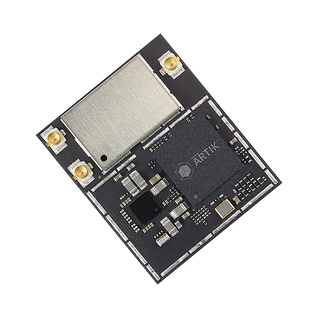
Samsung’s ARTIK™ 520 Module is a highly-integrated System-in®
®
Module that utilizes a dual core ARM Cortex -A7 processor
packaged DRAM and Flash memories, a Secure Element and a
wide range of wireless communication options such as
®
802.11a/b/g/n/ac, Bluetooth 4.1, Bluetooth Low Energy (BLE),
®
and 802.15.4/ZigBee communications all into a 30x25mm
footprint. The many standard digital control interfaces support
external sensors and higher performance peripherals to expand
the module capabilities.
With the combination of Wi-Fi,
Bluetooth and ZigBee the ARTIK 520 Module is the perfect choice
for home automation and home hub devices, while also
supporting a rich UI/UX capability with the camera and display
options. The hardware based Secure Element works with the
®
ARM TrustZone and Trustonic’s Trusted Execution Environment
(TEE) to provide “bank level” security end-to-end.
SAMSUNG ELECTRONICS RESERVES THE RIGHT TO CHANGE PRODUCTS, INFORMATION AND SPECIFICATIONS WITHOUT NOTICE.
Products and specifications discussed herein are for reference purposes only. All information discussed herein is provided on an "AS IS" basis, without warranties
of any kind. This document and all information discussed herein remain the sole and exclusive property of Samsung Electronics. No license of any patent,
copyright, mask work, trademark or any other intellectual property right is granted by one party to the other party under this document, by implication, estoppel
or other-wise. Samsung products are not intended for use in life support, critical care, medical, safety equipment, or similar applications where product failure
could result in loss of life or personal or physical harm, or any military or defense application, or any governmental procurement to which special terms or
provisions may apply. For updates or additional information about Samsung products, contact your nearest Samsung office. All brand names, trademarks and
registered trademarks belong to their respective owners.
�Samsung Semiconductor, Inc.
ARTIK 520 Module Data Sheet
Version History.................................................................................................................................................................. 6
ARTIK 520 Module ZigBee ................................................................................................................................................ 9
ARTIK 520 Module ZigBee Front End .............................................................................................................................. 9
ARTIK 520 Module PMIC .................................................................................................................................................. 9
ARTIK 520 Module Wi-Fi/Bluetooth .............................................................................................................................. 10
ARTIK 520 Module Secure Element ............................................................................................................................... 10
ARTIK 520 Module Secure JTAG ..................................................................................................................................... 11
ARTIK 520 Module Processor System ........................................................................................................................... 11
USB ................................................................................................................................................................................... 23
Audio Codec .................................................................................................................................................................... 23
UARTS ............................................................................................................................................................................... 24
Camera ............................................................................................................................................................................ 24
SD Card ............................................................................................................................................................................ 24
Power/Reset .................................................................................................................................................................... 25
LCD ................................................................................................................................................................................... 25
Ethernet Controller ......................................................................................................................................................... 26
Arduino ............................................................................................................................................................................ 27
Test Points ....................................................................................................................................................................... 27
SigFox ............................................................................................................................................................................... 28
Debug ............................................................................................................................................................................... 28
Absolute Maximum Ratings .......................................................................................................................................... 36
Recommended Operating Conditions .......................................................................................................................... 36
DC Module Use Case Characteristics ........................................................................................................................... 37
Power Supply Requirements ......................................................................................................................................... 37
ESD Ratings ..................................................................................................................................................................... 40
DC Electrical Characteristics ......................................................................................................................................... 41
AC Electrical Characteristics .......................................................................................................................................... 45
RF Electrical Characteristics .......................................................................................................................................... 50
�Samsung Semiconductor, Inc.
ARTIK 520 Module Data Sheet
Figure 1. ARTIK 520 Module Functional Block Diagram ......................................................................................................7
Figure 2. ARTIK 520 Module – Top View / Bottom View ......................................................................................................8
Figure 3. Processor System Block Schematic .................................................................................................................... 12
Figure 4. ARTIK 520 Module Connectors ............................................................................................................................ 16
Figure 5. ARTIK 520 Module Booting Sequence ................................................................................................................ 33
Figure 6. Hirose RF Connector for BT/Wi-Fi and ZigBee................................................................................................... 35
Figure 7. ARTIK 520 Module Power Distribution ............................................................................................................... 37
Figure 8. High Speed SDMMC Interface Timing ................................................................................................................ 45
Figure 9. SPI Interface Timing (CPHA = 0, CPOL = 1 (Format A)) ..................................................................................... 46
2
Figure 10. I C Interface Timing ............................................................................................................................................ 49
Figure 11. Mechanical Dimensions ..................................................................................................................................... 57
Table 1. Connector J3 ............................................................................................................................................................ 17
Table 2. Connector J4 ............................................................................................................................................................ 19
Table 3. Connector J5 ............................................................................................................................................................ 21
Table 4. USB ........................................................................................................................................................................... 23
Table 5. Audio Codec ............................................................................................................................................................ 23
Table 6. UARTS ....................................................................................................................................................................... 24
Table 7. Camera ..................................................................................................................................................................... 24
Table 8. SD Card .................................................................................................................................................................... 24
Table 9. Power/Reset ............................................................................................................................................................ 25
Table 10. LCD ......................................................................................................................................................................... 25
Table 11. Ethernet Controller .............................................................................................................................................. 26
Table 12. Arduino .................................................................................................................................................................. 27
Table 13. Test Points ............................................................................................................................................................. 27
Table 14. SigFox ..................................................................................................................................................................... 28
Table 15. Debug ..................................................................................................................................................................... 28
Table 16. Type A GPIO Alternate Functions Connector J3 ............................................................................................... 29
Table 17. Type A GPIO Alternate Functions Connector J4 ............................................................................................... 30
Table 18. Type B GPIO Alternate Functions Connector J4 ............................................................................................... 30
Table 19. Type A GPIO Alternate Functions Connector J5 ............................................................................................... 31
Table 20. Booting Options.................................................................................................................................................... 32
Table 21. Required Functions per Reset Type ................................................................................................................... 34
Table 22. Absolute Maximum Ratings ................................................................................................................................ 36
Table 23. Recommended Operating Conditions ............................................................................................................... 36
Table 24. Buck Description and Default Setting ................................................................................................................ 37
Table 25. PMIC LDOs ............................................................................................................................................................. 38
�Samsung Semiconductor, Inc.
ARTIK 520 Module Data Sheet
Table 26. AC/DC Characteristics LDO18 ............................................................................................................................. 39
Table 27. ESD Ratings ........................................................................................................................................................... 40
Table 28. Shock and Vibration Ratings ............................................................................................................................... 40
Table 29. I/O DC Electrical Characteristics ......................................................................................................................... 41
Table 30. I/O DC Electrical Characteristics ZIGBEE ........................................................................................................... 42
Table 31. I/O DC Electrical Characteristics PMIC ............................................................................................................... 42
Table 32. I/O DC Electrical Characteristics USB ................................................................................................................. 42
Table 33. Type A I/O Driver Strength and Delay Time ...................................................................................................... 43
Table 34. Type A I/O Pull-up/Down Resistor ...................................................................................................................... 43
Table 35. Type B I/O Output Cell Delay Time .................................................................................................................... 43
Table 36. Type B I/O Pull Up/Down Controller .................................................................................................................. 44
Table 37. Power on Reset Timing Specifications ............................................................................................................... 44
Table 38. High Speed SDMMC Interface Transmit/Receive Timing Constants ............................................................. 45
Table 39. SPI Interface Transmit/ Receive Timing Constants with 15pF Load .............................................................. 47
Table 40. SPI Interface Transmit/ Receive Timing Constants with 30pF Load .............................................................. 48
2
Table 41. I C BUS Controller Module Signal Timing.......................................................................................................... 49
Table 42. Wi-Fi WLAN 2.4GHz Receiver RF Specifications ................................................................................................ 50
Table 43. Wi-Fi WLAN 2.4GHz Transmitter RF Specifications .......................................................................................... 52
Table 44. Bluetooth RF Specifications ................................................................................................................................ 53
Table 45. ZigBee RF Receive Specifications ........................................................................................................................ 54
Table 46. ZigBee Transmit Specifications........................................................................................................................... 55
Table 47. Connectors J3, J4, J5 .............................................................................................................................................. 56
�Samsung Semiconductor, Inc.
Revision
Date
1.07
10/19/2016
ARTIK 520 Module Data Sheet
Description
ARTIK 520 Module Data Sheet
Maturity
Release
�Samsung Semiconductor, Inc.
ARTIK 520 Module Data Sheet
®
®
Figure 1 shows the functional block diagram of the ARTIK 520 Module. It consists of a dual-core ARM Cortex -A7
application processor with 512MB DRAM and 4GB eMMC Flash, PMIC, Secure Element, Wi-Fi/BT chipset, ZigBee
chipset, RF connectors and socket-type connectors.
ARTIK 520 MODULE
100x GPIO
(MUXED)
AUDIO
1x PCM, 1x I2S
1x JTAG
2.5x UART
1x SD CARD
SECURE
ELEMENT
2x ANALOG
POWER
MANAGEMENT
Wi-Fi
802.11a/b/g/n/ac
SYSTEM PROCESSORS
2x A7 @ 1GHz
32kB/32kB per Core
1MB L2 Cache
LPDDR3
512MB ePOP
BLUETOOTH
4.1+LE
802.15.4
ZIGBEE
FLASH
4GB ePOP
2x SPI
6x I2C
1x LCD
1x CAMERA
1x I2C
1x USB2.0
�Samsung Semiconductor, Inc.
ARTIK 520 Module Data Sheet
®
The top side is populated with the ARM application processor, PMIC, Wi-Fi/BT combo chipset and RF connectors
for Wi-Fi/BT and ZigBee antenna. The bottom side is populated with the ZigBee chipset, ZigBee front-end for RF
and Secure Element, two main connectors for function connection to main set and one debug connector for
debug interface connection.
J3
J3
PMIC
SE
J5
J5
ZIGBEE
Wi-Fi
BT
ARM®
PROCESSOR
J4
FE
J4
�Samsung Semiconductor, Inc.
ARTIK 520 Module Data Sheet
®
The ARTIK 520 Module carries a fully-integrated ZigBee unit called the Ember EM3587. It integrates a 2.4 GHz,
®
®
IEEE 802.15.4-2003-compliant transceiver, 32-bit ARM Cortex -M3 microprocessor, flash and RAM memory and
peripherals. The most important hardware features of the ZigBee module are:
®
®
Complete system-on-chip using 32-bit ARM Cortex -M3 processor.
Low power consumption:
RX current typical 27mA
TX current typical 31mA
Deep sleep current ≤ 1.25µA
RF performance:
Normal mode link budget up to 110dB
RX sensitivity up to 102dBm
Robust Wi-Fi and Bluetooth coexistence
Single-voltage operation
For more information on EM3587 contact a sales representative from Silicon Laboratories, Inc.
The ARTIK 520 Module carries a fully integrated RF Front-End Module (FEM) designed specifically for ZigBee
Smart Energy IoT environments. The device provides integrated and fully matched input baluns, an integrated
inter-stage matching and harmonic filter, and digital controls compatible with 1.6 to 3.6 V CMOS levels. The RF
blocks of the SE2432L support a wide range supply voltage tailored toward battery operated environments. The
most important hardware features of the ZigBee front-end are:
Integrated Power Amplifier up to 24dBm
Integrated Low-Noise Amplifier with programmable bypass
Integrated antenna switching, with transmit and receive diversity function
Low NF, 2dB typical
Differential transmit/receive interface with integrated baluns
Fast-switch on/off time ≤ 800ns
Sleep-mode current ≤ 0.05µA
For more information on SE2432L contact a sales representative from Skyworks Solutions, Inc.
The ARTIK 520 Module has a fully-integrated PMIC containing 5 Bucks and 25 LDOs. This unit provides all power
requirements for the ARTIK 520 Module in one compact form factor. In addition, various stable power outputs
are offered at the connectors, such that additional customer-defined use cases can be defined and efficiently
implemented.
For more information on S2MPS14 contact a sales representative from Samsung Semiconductor, Inc.
�Samsung Semiconductor, Inc.
ARTIK 520 Module Data Sheet
The ARTIK 520 Module has a fully-integrated MIMO combo BCM4354 for IEEE 802.11 a/b/g/n/ac wireless LAN
with Bluetooth 4.0+LE and FM. The most important hardware features of the Wireless/Bluetooth combo module
are:
WLAN 802.11ac compliant:
Single-stream spatial multiplexing up to 433Mbps
Support for 20, 40 and 80 MHz channels with optional SGI (256 QAM modulation)
WLAN 802.11 a/b/g/n/ac compliant
Bluetooth 4.0+LE
2G and 5G MIMO support
FM Receiver, 65MHz-108MHz bands
For more information on BCM 4354 contact a sales representative from Broadcom Ltd.
The ARTIK 520 Module has a dedicated Secure Element to assure end-to-end authentication and communication
between nodes in an IoT setting. The most important hardware features of the Secure Element are:
Dedicated secure CPU SC300
Crypto Accelerator
Hardware based AES/DES/3DES
TORNADO-E
5KB crypto RAM
Crypto co-processor
Modular exponential accelerator
RSA 4128bits/ECC 544 bits
Data security
Abnormal-condition detectors for: reset, interrupt, voltage, temperature, laser exposure, shield removal
Random Wait Generator, Random Current Generator
Secure optimized layout
Dynamic bus encryption
Embedded tamper-free memory
1.5MB flash (program and data)
32KB MASK ROM
48KB Static RAM
5KB Crypto RAM
Memory Protection Unit with 4GB addressable space
Secure flash write operation with fast page (0.5ms) and sector erase (4ms)
500K erase/write cycles/s
Serial interfaces:
2
I C/SPI/UART (ISO 7816)
A guaranteed 25 years data retention at room temperature
For more information on S3FV5RP contact a sales representative from Samsung Semiconductor, Inc.
�Samsung Semiconductor, Inc.
ARTIK 520 Module Data Sheet
Our secure JTAG core that is part of the ARTIK 520 Module provides debug capabilities for the developer. The
secure JTAG core authenticates the legal user. In addition, it provides an access level that the legal user can
operate under. The main features of the secure JTAG core are:
Dedicated authentication process through password
Dedicated Hash engine (SHA-1) with hash sequencer
Two access levels “access-on” and “access-off”
Industry standard JTAG capabilities
The processor system architecture that resides on the ARTIK 520 Module is a system-on-a-chip (SoC) based on a
32-bit RISC processor. Designed using the 28nm low power process, the processor system architecture provides
®
superior performance using a dual-core CORTEX -A7 CPU. The ARTIK 520 Module contains 3D graphics
hardware, image signal-processor hardware and a variety of high-speed interfaces such as eMMC5.0.
®
The ARTIK 520 Module contains the dual Cortex -A7. The ARTIK 520 Module allows for heavy traffic operations
such as
720p video encoding/decoding, 3D graphics display and high resolution image signal processing.
The application processor supports dynamic virtual-address mapping aiding software engineers to fully utilize
the memory resources. The key features of the ARTIK 520 Module are:
®
®
Dual-core ARM Cortex -A7, 32 KB I$/32 KB D$ and 1MB L2 Cache
128-bit multi-layer AXI bus architecture
Internal ROM and RAM for secure booting and general-use purposes
Memory subsystem:
1-port 32-bit 400MHz LPDDR2/LPDDR3 interface
Supports 3D and 2D graphics hardware
LCD single qHD display supports MIPI
Support for 2-lane MIPI DSI interface
Support for 2-lane MIPI CSI interface
2
Support for 1-channel PCM and 1-channel 24-bit I S audio interface
2
2
Support for 6-channel I C general-purpose multi-master interface and 1-channel dedicated camera I C
interface
Support for 2-channel high-speed SPI interface
Support for 2.5-channel high-speed UART (up to 3Mbps data rate for Bluetooth 2.1 EDR and IrDA 1.0 SIR)
Support for USB 2.0, 1-channel supports LS/FS/HS (1.5Mbps/12Mbps/480Mbps) with on-chip PHY
Support for 2-channel SD/MMC interface supports SDIO3.0, eMMC5.0 DDR with 8-bit interface
Support for up to 100 configurable GPIO (multiplexed)
Real time clock, PLLs, timer with PWM, and watchdog timer
Support for 2-channel (multiplexed) general-purpose ADC
�Samsung Semiconductor, Inc.
ARTIK 520 Module Data Sheet
PROCESSOR SYSTEM
Display/Camera
Cortex-A7 Dual
LCD DSI up to
960x540@24bpp
CPU 0
1.0 GHz
32kB/32kB
DMC
LPDDR2-S4 533MHz
LPDDR3 @ 667MHZ
CPU 1
1.0 GHz
32kB/32kB
SRAM/NOR/ROM
SCU
CAMERA CSI up to
3MP@30fps
DDR3
1MB L2 Cache
High Speed I/F
Secure
256KB SRAM
Secure
64KB ROM
Multi Media
Low Power Multi-Layer AXI/AHB Bus
Mali-400MP2
Series
USB 2.0
CCI
External Peripherals
I2C
ADC
GPIO
SD/SDIO/
eMMC5.0
2-ch
JPEG Codec
SPI
UART
I2S/PCM
The ARTIK 520 Module provides 1x 2-lane MIPI interface that complies with the MIPI DSI standard specification
V1.01r11. The key features of the MIPI DSI sub-system are:
Maximum resolution ranges up to qHD (960x540@24bpp)
Supports 1 or 2 data lanes.
Supported interfaces are:
Protocol-to-PHY Interface (PPI) in MIPI D-PHY specification V0.90
RGB Interface for video image input from display controller
An I80 interface for Command Mode Image input from display controller
PMS control interface for PLL to configure byte clock frequency
Pre-scaler to generate escape clock from byte clock
The ARTIK 520 Module provides 1x 2-lane MIPI interface that complies with the MIPI CSI standard specification
V1.01r06. The key features of the MIPI CSI sub-system are:
Supports 1 or 2 data lanes
�Samsung Semiconductor, Inc.
ARTIK 520 Module Data Sheet
Supports up to 3MP@30fps
Supported image formats are:
YUV420, YUV420 (Legacy), YUV420 (CSPS), 8-bit YUV422, 10-bit YUV422
MJPEG
The ARTIK 520 Module provides 2x Serial Peripheral Interfaces (SPI) that transfers serial data. SPI support
includes
8-bit/16-bit/32-bit shift registers to transmit and receive data. During an SPI transfer, data is simultaneously
transmitted (shifted out serially) and received (shifted in serially). The SPI implementation adheres to the
protocols described by National Semiconductor, Microwire and Motorola’s Serial Peripheral Interface. The key
features of the SPI sub-system are:
Support for full-duplex
8-bit/16-bit/32-bit shift register for Tx and Rx
8-bit/16-bit/32-bit bus interface
Complies with the SPI protocol described by National Semiconductor, Microwire and Motorola
Support for 2 independent 32-bit wide transmit and receive FIFOs:
Depth 64 in SPI port 0 and depth 16 in SPI port 1
Supports for master mode and slave mode
Supports for receive-without-transmit operation
Support Tx/Rx up to 50 MHz
The ADC interface controls one 28nm low power CMOS 1.8V 12-bit ADC. It converts the analog input signal into
12-bit binary code at a conversion rate of 50kSPS-1MSPS with a 1MHz-20MHz main clock. The ADCIF includes a
12-bit resolution that combines with an analog input multiplexer. The analog input multiplexer selects one from
2 input channels.
The ARTIK 520 Module provides 2x full 4-pin UARTs plus 1x 2-pin UART with just RxD and TxD signals. The key
features of the UART sub-system are:
Both DMA and interrupt based mode of operation supported
All independent channels support IrDA 1.0
Each UART channel contains two FIFOs to receive and transmit data:
256 bytes in ch0 and ch2
64 bytes in ch1
16 bytes in ch3
Each UART channel contains:
Programmable baud-rates
One or two stop bit insertion
5-bit, 6-bit, 7-bit, or 8-bit data width
Parity checking
2
2
The ARTIK 520 Module provides one 3-line Inter-IC Sound (I S) channel. I S is one of the most popular digital
2
audio interfaces. The I S bus handles audio data and other signals, such as sub-coding and control.
2
It is possible to transmit data between two I S buses. To minimize the number of pins required and to keep
2
wiring simple, a 3-line serial bus is used. The key features of the I S sub-system are:
�Samsung Semiconductor, Inc.
ARTIK 520 Module Data Sheet
2
Supports 1-port stereo (1 channel) I S-bus for audio with DMA based operation
Supports serial data transfer of 8/16/24-bit per channel
2
Supports I S, MSB-justified, and LSB-justified data formats
Supports both master and slave modes
The ARTIK 520 Module provides 1x PCM channel. The PCM audio interface provides a bi-directional serial
interface
to an external codec. The key features of the PCM sub-system are:
A 16-bit PCM with 1 port audio interface
Supports only Master mode
All PCM serial timings and strobes are extracted from one master clock
Supports 1x input (16-bit x 32depth) and 1x output (16-bit x 32 depth) FIFO to buffer data
DMA interface for Tx or Rx or both
The ARTIK 520 Module provides a GPIO system to allow for a wide variety of use cases to be supported. The key
features of the GPIO system are:
Control for up to 91 external interrupts
Falling edge triggered
Rising edge triggered
Both edge triggered
Control for up to 25 wake-up interrupts
Falling edge triggered
Rising edge triggered
Both edge triggered
Control for up to 100 General Purpose I/Os
Controls a variety of pin states in sleep mode
2
2
The ARTIK 520 Module provides 6x generic 400kb/s I C channels + 1x dedicated 400kb/s camera I C channel.
2
The key features of the I C sub-system are:
Supporting master and slave mode
7-bit addressing mode only
Supports serial, 8-bit oriented and bi-directional data transfer
Supports up to 100 kb/s in the standard mode
Supports up to 400 kb/s in the fast mode
Supports master transmit, master receive, slave transmit, and slave receive operation
Supports both interrupt and polling events
The ARTIK 520 Module provides one USB2.0 interface. The key features of the USB2.0 sub-system are:
In compliance with the USB 2.0 specification revision 1.0a
In compliance with the UTMI+ Level3 revision 1.0
Supports high-speed and full-speed transfers
Supports up to 15 device-programmable endpoints:
Programmable endpoint type: Bulk, Isochronous, Interrupt
Programmable In/Out direction
�Samsung Semiconductor, Inc.
ARTIK 520 Module Data Sheet
Supports packet-based dynamic FIFO memory allocation up to 7936 depth
The ARTIK 520 Module provides one SDIO/xMMC interface. The Mobile Storage Host is an interface between the
system and SD/MMC card. This host supports 8-bit DDR transfer with a 200 MHz clock rate. The key features of
mobile storage host sub-system are:
Support for Embedded Multimedia Cards (eMMC – version 5.0)
Support for Embedded Multimedia Cards (eMMC – version 4.5)
Support for Secure Digital I/O (SDIO – version 3.0)
Support for Consumer Electronics Advanced Transport Architecture (CE-ATA – version 1.1)
Support for Multimedia Cards (MMC – version 4.4)
®
The ARTIK 520 Module provides 1x instance of the Mali™-400 GPU series from ARM . The Mali™-400 series adds
graphics capabilities to the ARTIK 520 Module. The key features of the Mali™-400 sub-system are:
Resolution of 4kx4k for the frame buffer as well as the texture buffer
Tile-based pixel processing
Scalable multi-core pixel processors (128 threads)
The ARTIK 520 Module provides a Dynamic Memory Controller (DMC) that is compatible with the JEDEC standard
supporting LPDDR3/DDR3 and SDRAM devices. The following memory interfaces are supported:
LPDDR2-S4 up to 533MHz
LPDDR3 up to 667 MHz
DDR3
®
®
The ARTIK 520 Module provides 2xCPU cores which consist of ARM Cortex -A7 core processors. For easier and
faster CPU core switching, the ARTIK 520 Module supports a cache coherency interconnect (CCI) bus with L2
®
®
cache snooping capability. The ARM Cortex -A7 dual-core has the following common features:
®
®
Common ARM v7-A Cortex architecture
A core speed up to 1GHZ
Security Extensions for implementation of enhanced security
Virtualization Extensions for the development of virtualized systems that enable switching guest operation
systems
Program Trace Macrocell that is ARM CoreSight compatible
®
Multi-core ARM TrustZone technology
�Samsung Semiconductor, Inc.
ARTIK 520 Module Data Sheet
The ARTIK 520 Module utilizes three 60-position connectors for all power, analog and digital I/O. Connectors J3,
J4 and J5 are Panasonic ATX460124 with 60 pins and 0.4mm pitch.
shows the power/signal name
assigned to each pin of each connector.
,
and
describe the pinout in detail.
CONNECTOR J3
CONNECTOR J4
CONNECTOR J5
MAIN_BAT
1
2
MAIN_BAT
XspiCLK0
1
2
AP_USB_DM
GND
1
2
GND
MAIN_BAT
3
4
MAIN_BAT
XspiCSn0
3
4
AP_USB_DP
EBI_OEn
3
4
GPM3_1
GND
5
6
GND
XspiMISO0
5
6
GND
EBI_Wen
5
6
GPM3_0
GND
7
8
GND
XspiMOSI0
7
8
AP_USB_VBUS
EBI_CSn
7
8
GND
XGPIO15
9
10
PWR_KEY
PSR_TE
9
10
GND
9
10
XjTCK
XEINT_14
11 12
XEINT_13
Xi2c7_SDA
11 12
GPM4_4
EBI_ADDR0
11 12
XjTDI
XEINT_16
13 14
XEINT_12
Xi2c7_SCL
13 14
GPM4_5
EBI_ADDR1
13 14
XjTDO
XEINT_17
15 16
XEINT_8
Xi2c1_SCL
15 16
GPM4_6
EBI_ADDR2
15 16
XjTMS
XEINT_18
17 18
DRD_VBUS_SENSE_0
Xi2c1_SDA
17 18
GPM4_7
EBI_ADDR3
17 18
XjTRSTn
XEINT_20
19 20
XEINT_6
VTCAM_RESET
19 20
GND
EBI_ADDR4
19 20
GND
XEINT_21
21 22
XEINT_5
XISP2_SCL0
21 22
DISP_MIPI_D0_N EBI_ADDR5
21 22
32768HZ
XEINT_24
23 24
XEINT_4
XISP2_SDA0
23 24
DISP_MIPI_D1_P
EBI_ADDR6
23 24
GND
XEINT_25
25 26
XEINT_3
GND
25 26
GND
GND
25 26
DEBUG_RXD
XEINT_27
27 28
XEINT_2
VTCAM_D0_N
27 28
DISP_MIPI_D1_N
EBI_DAT0
27 28
DEBUG_TXD
XEINT_28
29 30
XEINT_1
VTCAM_D0_P
29 30
DISP_MIPI_D1_P
EBI_DAT1
29 30
GND
V_ADP_SENSE
31 32
XEINT_0
GND
31 32
GND
EBI_DAT2
31 32
XspiCLK1
GND
33 34
XGPIO17/XT_INT163 VTCAM_D1_N
33 34
DISP_MIPI_CLK_N
EBI_DAT3
33 34
XspiCSn1
XOM2
35 36
GND
VTCAM_D1_P
35 36
DISP_MIPI_CLK_P
EBI_DAT4
35 36
XspiMISO1
XOM3
37 38
Xu3_RXD
GND
37 38
GND
EBI_DAT5
37 38
XspiMOSI1
XGPIO6
39 40
Xu3_TXD
VTCAM_CLK_N
39 40
XMMC2CDN
EBI_DAT6
39 40
GND
XEINT_22
41 42
GND
VTCAM_CLK_P
41 42
XMMC2CLK
EBI_DAT7
41 42
VLDO18
XUART_SCLK
43 44
Xadc0AIN0
GND
43 44
XMMC2CMD
EBI_DAT8
43 44
VLDO18
XUART_MOSI
45 46
Xadc0AIN1
Xpwmo_1
45 46
XMMC2DATA0
EBI_DAT9
45 46
ZB_PC2
XUART_MISO
47 48
XAudi2s2SDO
Xpwmo_0
47 48
XMMC2DATA1
EBI_DAT10
47 48
ZB_PC0
XUART_CS
49 50
XAudi2s2SDI
COIN_BATT
49 50
XMMC2DATA2
EBI_DAT11
49 50
ZB_PC3
GND
51 52
XAudi2s2SCLK
AP_NRESET
51 52
XMMC2DATA3
EBI_DAT12
51 52
ZB_JTCK
XCLKOUT
53 54
XAudi2s2LRCK
Xi2c3_SCL
53 54
GND
EBI_DAT13
53 54
ZB_PC4
GND
55 56
XAudi2s2CDCLK
Xi2c3_SDA
55 56
GPC0_4
EBI_DAT14
55 56
ZB_RSTN
XEINT_9
57 58
GND
LCD_RST
57 58
AP_NWRESET
EBI_DAT15
57 58
ZB_PA4
VTCAM_PDN
59 60
CODEC_PDN
XGPIO3
59 60
XGPIO2
GND
59 60
ZB_PA5
USB_ID
�Samsung Semiconductor, Inc.
ARTIK 520 Module Data Sheet
Connector J3
DS
PUD*
[mA]
Conn#
Pin#
Name
I/O
I/O Type
Voltage
Group
Function
J3
1
MAIN_BAT
NA
NA
3V8
NA
J3
3
MAIN_BAT
NA
NA
3V8
NA
NA
NA
Main battery
NA
NA
Main battery
J3
5
GND
NA
NA
0V0
J3
7
GND
NA
NA
0V0
NA
NA
NA
Ground
NA
NA
NA
Ground
PDE
ETHERNET
CONTROLLER
External chip GPIO1
J3
9
XGPIO15
I
A
1V8
2
J3
11
XEINT_14
I
A
1V8
2
PUE
ARDUINO
General purpose interrupt or IO
ETHERNET
CONTROLLER
External chip IRQ
J3
13
XEINT_16
I
A
1V8
2
PUD
D
J3
15
XEINT_17
I
A
1V8
2
PUD
D
POWER/RESET
Charge status interrupt
J3
17
XEINT_18
I
A
1V8
2
PUD
D
UART
SPI-TO-UART IC for SPI bus emulation
RESET
J3
19
XEINT_20
I
A
1V8
2
PUD
D
UART
SPI-TO-UART IC for SPI bus emulation
IRQ
J3
21
XEINT_21
O
A
1V8
2
PUD
D
LCD
Backlight enable
J3
23
XEINT_24
I
A
1V8
2
PDE
POWER/RESET
Turn device on
J3
25
XEINT_25
I
A
1V8
2
PDE
POWER/RESET
Fuel gauge interrupt
J3
27
XEINT_27
I
A
1V8
2
PDE
AUDIO
Ear microphone detect
2
PDE
ETHERNET
CONTROLLER
External chip CS
J3
29
XEINT_28
I
A
1V8
J3
31
J3
33
V_ADP_SENSE
I
A/SE
1V8
2
PDE
POWER/RESET
AC Power detect
GND
NA
NA
0V0
NA
NA
NA
Ground
J3
J3
35
XOM2
I
NA
1V8
NA
NA
POWER/RESET
SD/MMC or eMMC boot
37
XOM3
I
NA
1V8
NA
NA
POWER/RESET
J3
SD/MMC or eMMC boot
39
XGPIO6
I
A
1V8
2
PDE
ZWAVE
SD3503 ZWAVE reset
CAMERA
27MHz osc enable
J3
41
XEINT_22
I
A
1V8
2
PUD
D
J3
43
XUART_SCLK
I
A
1V8
2
PDE
UARTS
SPI-TO-UART IC for SPI bus emulation
SCLK
J3
45
XUART_MOSI
I
A
1V8
2
PDE
UARTS
SPI-TO-UART IC for SPI bus emulation
MOSI
J3
47
XUART_MISO
I
A
1V8
2
PDE
UARTS
SPI-TO-UART IC for SPI bus emulation
MISO
J3
49
XUART_CS
I
A
1V8
2
PDE
UARTS
SPI-TO-UART IC for SPI bus emulation
CS
J3
51
GND
NA
NA
0V0
NA
NA
NA
Ground
1V8
NA
NA
AUDIO
Clock
0V0
NA
NA
NA
Ground
2
PDE
ETHERNET
CONTROLLER
General purpose interrupt or IO
J3
53
XCLKOUT
O
PROCESSO
R
J3
55
GND
NA
NA
J3
57
XEINT_9
J3
59
VTCAM_PDN
J3
2
MAIN_BAT
J3
4
MAIN_BAT
J3
6
GND
J3
8
J3
10
I
A
1V8
I
A
1V8
2
PDE
CAMERA
Power down
NA
NA
3V8
NA
NA
NA
Main battery
NA
NA
3V8
NA
NA
NA
Main battery
NA
NA
0V0
NA
NA
NA
Ground
GND
NA
NA
0V0
NA
NA
NA
Ground
PWR_KEY
I
PMIC
NA
NA
NA
POWER/RESET
PMIC power on key
�Samsung Semiconductor, Inc.
ARTIK 520 Module Data Sheet
Connector J3
DS
PUD*
[mA]
Conn#
Pin#
Name
I/O
I/O Type
Voltage
Group
Function
J3
12
XEINT_13
I
A
1V8
2
PDE
ARDUINO
General purpose interrupt or IO
J3
14
XEINT_12
I
A
1V8
2
PDE
SIGFOX
Low power wireless transmitter reset
J3
16
XEINT_8
I
A
1V8
2
PDE
ARDUINO
General purpose interrupt or IO
J3
18
DRD_VBUS_SENSE
_0
I
A
1V8
2
PDE
USB
Device detect
J3
20
XEINT_6
I
A
1V8
2
PDE
ARDUINO
General purpose interrupt or IO
J3
22
XEINT_5
I
A
1V8
2
PDE
ARDUINO
General purpose interrupt or IO
J3
24
XEINT_4
I
A
1V8
2
PDE
ARDUINO
General purpose interrupt or IO
J3
26
XEINT_3
I
A
1V8
2
PUE
ARDUINO
General purpose interrupt or IO
J3
28
XEINT_2
I
A
1V8
2
PDE
ARDUINO
General purpose interrupt or IO
J3
30
XEINT_1
I
A
1V8
2
PDE
ARDUINO
General purpose interrupt or IO
J3
32
XEINT_0
I
A
1V8
2
PDE
ARDUINO
General purpose interrupt or IO
J3
34
XGPIO17/XT_INT1
63
I
A
1V8
2
PDE
POWER/RESET
External IC interrupt
J3
36
GND
NA
NA
0V0
NA
NA
NA
Ground
ARDUINO
RxD
ARDUINO
TxD
J3
38
Xu3_RXD
I
A
1V8
2
PUD
D
J3
40
Xu3_TXD
I
A
1V8
2
PUD
D
J3
42
GND
NA
NA
0V0
NA
NA
NA
Ground
J3
44
Xadc0AIN0
I
ADC
1V8
NA
NA
ARDUINO
Input 0
J3
46
Xadc0AIN1
I
ADC
1V8
NA
NA
ARDUINO
Input 1
J3
48
XAudi2s2SDO
I
A
1V8
2
PDE
AUDIO
SDO
J3
50
XAudi2s2SDI
I
A
1V8
2
PDE
AUDIO
SDI
J3
52
XAudi2s2SCLK
I
A
1V8
2
PDE
AUDIO
SCLK
J3
54
XAudi2s2LRCK
I
A
1V8
2
PDE
AUDIO
LRCLK
J3
56
XAudi2s2CDCLK
I
A
1V8
2
PDE
AUDIO
CDCLK
J3
58
GND
NA
NA
0V0
NA
NA
NA
Ground
AUDIO
AK4953EQ audio codec IC power
down
J3
60
CODEC_PDN
I
A
1V8
2
PDE
* The PUD variables have the following meaning: PUDD = Power Up Down Disabled, PDE = Power Down Enabled,
PUE = Power Up Enabled, R = Reserved.
�Samsung Semiconductor, Inc.
ARTIK 520 Module Data Sheet
Connector J4
Conn# Pin#
Name
I/O
I/O Type
Voltage
DS
[mA]
PUD
Group
Function
J4
1
XspiCLK0
I
A
1V8
2
PDE
ETHERNET
CONTROLLER/SIGFOX
SPI CLK
J4
3
XspiCSn0
I
A
1V8
2
PDE
ETHERNET
CONTROLLER/SIGFOX
SPI CSn
J4
5
XspiMISO0
I
A
1V8
2
PDE
ETHERNET
CONTROLLER/SIGFOX
SPI MISO
J4
7
XspiMOSI0
I
A
1V8
2
PDE
ETHERNET
CONTROLLER/SIGFOX
SPI MOSI
J4
9
PSR_TE
I
A
1V8
2
PDE
LCD
CLK
J4
11
Xi2c7_SDA
I
A
1V8
2
PDE
ARDUINO
General purpose I2C SDA
J4
13
Xi2c7_SCL
I
A
1V8
2
PDE
ARDUINO
General purpose I2C SCL
J4
15
Xi2c1_SCL
I
A
1V8
2
PDE
AUDIO/POWER/RESET
I2C SCL
J4
17
Xi2c1_SDA
I
A
1V8
2
PDE
AUDIO/POWER/RESET
I2C SDA
J4
19
VTCAM_RESET
O
A
1V8
2
PDE
CAMERA
RESET Camera
J4
21
XISP2_SCL0
I
A
1V8
2
PDE
CAMERA
I2C SCL
J4
23
XISP2_SDA0
I
A
1V8
2
PDE
CAMERA
I2C SDA
J4
25
GND
NA
NA
0V0
NA
NA
NA
Ground
J4
27
VTCAM_D0_N
I/O
MIPI
1V0
NA
NA
CAMERA
MIPI D0_N
J4
29
VTCAM_D0_P
I/O
MIPI
1V0
NA
NA
CAMERA
MIPI D0_P
J4
31
GND
NA
NA
0V0
NA
NA
NA
Ground
J4
33
VTCAM_D1_N
I/O
MIPI
1V0
NA
NA
CAMERA
MIPI D1_N
J4
35
VTCAM_D1_P
I/O
MIPI
1V0
NA
NA
CAMERA
MIPI D1_P
J4
37
GND
NA
NA
0V0
NA
NA
NA
Ground
J4
39
VTCAM_CLK_N
I/O
MIPI
1V0
NA
NA
CAMERA
MIPI CLK_N
J4
41
VTCAM_CLK_P
I/O
MIPI
1V0
NA
NA
CAMERA
MIPI CLK_P
J4
43
GND
NA
NA
0V0
NA
NA
NA
Ground
J4
45
Xpwmo_1
I
A
1V8
2
PDE
ARDUINO
General purpose interrupt or IO
or PWM
J4
47
Xpwmo_0
I
A
1V8
2
PDE
ARDUINO
General purpose interrupt or IO
or PWM
J4
49
COIN_BAT
NA
PMIC
3V0
NA
NA
POWER/RESET
Backup battery
J4
51
AP_NRESET
I
PROCESS
OR/PMIC
1V8
NA
NA
POWER/RESET/
ARDUINO/JTAG
ARTIK 520 Module reset
J4
53
Xi2c3_SCL
I
A
1V8
2
PUDD
TEST POINTS
I2C SCL
J4
55
Xi2c3_SDA
I
A
1V8
2
PUDD
TEST POINTS
I2C SDA
J4
57
LCD_RST
O
A
1V8
2
PDE
LCD
Reset
J4
59
XGPIO3
I
A
1V8
2
PDE
ETHERNET CONTROLLER
External Chip GPIO0
J4
2
AP_USB_DM
I/O
USB2.0
3V0
NA
NA
USB
USB DM
J4
4
AP_USB_DP
I/O
USB2.0
3V0
NA
NA
USB
USB DP
J4
6
GND
NA
NA
0V0
NA
NA
NA
Ground
J4
8
AP_USB_VBUS
I/O
USB2.0
3V0
NA
NA
USB
USB VBUS
J4
10
USB_ID
I
USB2.0
3V0
NA
NA
USB
ID
J4
12
GPM4_4
I
A
1V8
2
PDE
SIGFOX
ATA8520 SPI bus emulation
J4
14
GPM4_5
I
A
1V8
2
PDE
SIGFOX
ATA8520 SPI bus emulation
J4
16
GPM4_6
I
A
1V8
2
PDE
SIGFOX
ATA8520 SPI bus emulation
J4
18
GPM4_7
I
A
1V8
2
PDE
SIGFOX
ATA8520 SPI bus emulation
J4
20
GND
NA
NA
0V0
NA
NA
NA
Ground
J4
22
DISP_MIPI_D0_N
I/O
MIPI
1V0
NA
NA
LCD
MIPI D0_N
�Samsung Semiconductor, Inc.
ARTIK 520 Module Data Sheet
Connector J4
Conn# Pin#
Name
I/O
I/O Type
Voltage
DS
[mA]
PUD
Group
Function
MIPI D0_P
J4
24
DISP_MIPI_D0_P
I/O
MIPI
1V0
NA
NA
LCD
J4
26
GND
NA
NA
0V0
NA
NA
NA
Ground
J4
28
DISP_MIPI_D1_N
I/O
MIPI
1V0
NA
NA
LCD
MIPI D1_N
J4
30
DISP_MIPI_D1_P
I/O
MIPI
1V0
NA
NA
LCD
MIPI D1_P
J4
32
GND
NA
NA
0V0
NA
NA
NA
Ground
J4
34
DISP_MIPI_CLK_N
I/O
MIPI
1V0
NA
NA
LCD
MIPI CLK_N
J4
36
DISP_MIPI_CLK_P
I/O
MIPI
1V0
NA
NA
LCD
MIPI CLK_P
J4
38
GND
NA
NA
0V0
NA
NA
NA
Ground
J4
40
XMMC2CDN
I
B
1V8
4
PUE
SD CARD
XMMC2 CDN
J4
42
XMMC2CLK
O
B
1V8
12
PUDD
SD CARD
XMMC2 CLK
J4
44
XMMC2CMD
O
B
1V8
12
PUDD
SD CARD
XMMC2 CMD
J4
46
XMMC2DATA0
I
B
1V8
12
PUE
SD CARD
XMMC2 DATA0
J4
48
XMMC2DATA1
I
B
1V8
12
PUE
SD CARD
XMMC2 DATA1
J4
50
XMMC2DATA2
I
B
1V8
12
PUE
SD CARD
XMMC2 DATA2
J4
52
XMMC2DATA3
I
B
1V8
12
PUE
SD CARD
XMMC2 DATA3
J4
54
GND
NA
NA
0V0
NA
NA
NA
Ground
J4
56
GPC0_4
I
A
1V8
2
PDE
LCD
Identification (ID)
J4
58
AP_NWRESET
I
PROCESS
OR/PMIC
1V8
NA
NA
PMIC
Warm reset from PMIC
(development purposes)
J4
60
XGPIO2
I
A
1V8
2
PDE
ETHERNET CONTROLLER
External chip reset
�Samsung Semiconductor, Inc.
ARTIK 520 Module Data Sheet
Connector J5
Name
I/O
I/O Type
Voltage
DS
[mA]
1
GND
NA
NA
0V0
NA
NA
NA
Ground
3
EBI_OEn
I
A
1V8
2
PDE
ETHERNET CONTROLLER
External chip RDN
J5
5
EBI_Wen
I
A
1V8
2
PDE
ETHERNET CONTROLLER
External chip WRN
J5
7
EBI_CSn
I
A
1V8
2
PDE
ETHERNET CONTROLLER
CS 1 default connect
Conn#
Pin#
J5
J5
PUD
Group
Function
J5
9
GND
NA
NA
0V0
NA
NA
NA
Ground
J5
11
EBI_ADDR0
I
A
1V8
2
PDE
ETHERNET CONTROLLER
External chip EBI_ADDR0
J5
13
EBI_ADDR1
I
A
1V8
2
PDE
ETHERNET CONTROLLER
External chip EBI_ADDR1
J5
15
EBI_ADDR2
I
A
1V8
2
PDE
ETHERNET CONTROLLER
External chip EBI_ADDR2
J5
17
EBI_ADDR3
I
A
1V8
2
PDE
ETHERNET CONTROLLER
External chip EBI_ADDR3
J5
19
EBI_ADDR4
I
A
1V8
2
PDE
ETHERNET CONTROLLER
External chip EBI_ADDR4
J5
21
EBI_ADDR5
I
A
1V8
2
PDE
ETHERNET CONTROLLER
External chip EBI_ADDR5
J5
23
EBI_ADDR6
I
A
1V8
2
PDE
NA
Not used
J5
25
GND
NA
NA
0V0
NA
NA
NA
Ground
J5
27
EBI_DAT0
I
A
1V8
2
PDE
ETHERNET CONTROLLER
EBI BUS DATA 0
J5
29
EBI_DAT1
I
A
1V8
2
PDE
ETHERNET CONTROLLER
EBI BUS DATA 1
J5
31
EBI_DAT2
I
A
1V8
2
PDE
ETHERNET CONTROLLER
EBI BUS DATA 2
J5
33
EBI_DAT3
I
A
1V8
2
PDE
ETHERNET CONTROLLER
EBI BUS DATA 3
J5
35
EBI_DAT4
I
A
1V8
2
PDE
ETHERNET CONTROLLER
EBI BUS DATA 4
J5
37
EBI_DAT5
I
A
1V8
2
PDE
ETHERNET CONTROLLER
EBI BUS DATA 5
J5
39
EBI_DAT6
I
A
1V8
2
PDE
ETHERNET CONTROLLER
EBI BUS DATA 6
J5
41
EBI_DAT7
I
A
1V8
2
PDE
ETHERNET CONTROLLER
EBI BUS DATA 7
J5
43
EBI_DAT8
I
A
1V8
2
PDE
ETHERNET CONTROLLER
EBI BUS DATA 8
J5
45
EBI_DAT9
I
A
1V8
2
PDE
ETHERNET CONTROLLER
EBI BUS DATA 9
J5
47
EBI_DAT10
I
A
1V8
2
PDE
ETHERNET CONTROLLER
EBI BUS DATA 10
J5
49
EBI_DAT11
I
A
1V8
2
PDE
ETHERNET CONTROLLER
EBI BUS DATA 11
J5
51
EBI_DAT12
I
A
1V8
2
PDE
ETHERNET CONTROLLER
EBI BUS DATA 12
J5
53
EBI_DAT13
I
A
1V8
2
PDE
ETHERNET CONTROLLER
EBI BUS DATA 13
J5
55
EBI_DAT14
I
A
1V8
2
PDE
ETHERNET CONTROLLER
EBI BUS DATA 14
J5
57
EBI_DAT15
I
A
1V8
2
PDE
ETHERNET CONTROLLER
EBI BUS DATA 15
J5
59
GND
NA
NA
0V0
NA
NA
NA
Ground
J5
2
GND
NA
NA
0V0
NA
NA
NA
Ground
J5
4
GPM3_1
I
A
1V8
2
PDE
TEST POINTS
Not used
J5
6
GPM3_0
I
A
1V8
2
PDE
TEST POINTS
Not used
J5
8
GND
NA
NA
0V0
NA
NA
NA
Ground
J5
10
XjTCK
I
JTAG
1V8
NA
NA
JTAG
JTAG CLK
J5
12
XjTDI
I
JTAG
1V8
NA
NA
JTAG
JTAG TDI
J5
14
XjTDO
O
JTAG
1V8
NA
NA
JTAG
JTAG TDO
J5
16
XjTMS
I
JTAG
1V8
NA
NA
JTAG
JTAG TMS
J5
18
XjTRSTn
I
JTAG
1V8
NA
NA
JTAG
JTAG RSTn
J5
20
GND
NA
NA
0V0
NA
NA
NA
Ground
32768HZ
O
PROCESS
OR/PMIC/
BT
1V8
NA
NA
TEST POINTS
32 KHz clock
J5
22
J5
24
GND
NA
NA
0V0
NA
NA
NA
Ground
J5
26
DEBUG_RXD
I
A
1V8
2
PUDD
DEBUG
AP debug UART RxD
J5
28
DEBUG_TXD
I
A
1V8
2
PUDD
DEBUG
AP debug UART TxD
J5
30
GND
NA
NA
0V0
NA
NA
NA
Ground
�Samsung Semiconductor, Inc.
ARTIK 520 Module Data Sheet
Connector J5
Name
I/O
I/O Type
Voltage
DS
[mA]
PUD
Group
32
XspiCLK1
O
A/SE
1V8
2
PDE
TEST POINTS
SPI CLK
34
XspiCSn1
O
A/SE
1V8
2
PDE
TEST POINTS
SPI CSn
J5
36
XspiMISO1
O
A/SE
1V8
2
PDE
TEST POINTS
SPI MISO
J5
38
XspiMOSI1
O
A/SE
1V8
2
PDE
TEST POINTS
SPI MOSI
J5
40
GND
NA
NA
0V0
NA
NA
NA
Ground
J5
42
VLDO18
NA
NA
2V8
NA
NA
JTAG
2.8V/300mA
J5
44
VLDO18
NA
NA
2V8
NA
NA
JTAG
2.8V/300mA
J5
46
ZB_PC2
O
ZIGBEE
1V8
NA
NA
JTAG
JTAG data out
J5
48
ZB_PC0
I
ZIGBEE
1V8
NA
NA
JTAG
JTAG reset
J5
50
ZB_PC3
I
ZIGBEE
1V8
NA
NA
JTAG
JTAG data in
J5
52
ZB_JTCK
I
ZIGBEE
1V8
NA
NA
JTAG
JTAG clock
J5
54
ZB_PC4
I
ZIGBEE
1V8
NA
NA
JTAG
JTAG mode select
J5
56
ZB_RSTn
O
ZIGBEE/LS
1V8
2
PDE
JTAG
JTAG reset
J5
58
ZB_PA4
I/O
ZIGBEE
1V8
NA
NA
JTAG
JTAG GPIO
J5
60
ZB_PA5
I/O
ZIGBEE/LS
1V8
NA
NA
JTAG
JTAG GPIO
Conn#
Pin#
J5
J5
Function
�Samsung Semiconductor, Inc.
ARTIK 520 Module Data Sheet
This section shows the functional interfaces that are available at the connectors. Since some of the functionality
is spread over multiple connectors, these tables will help provide better insight into what functionality is located
where. The functions provided are related to the development environment used. Depending on your project
you can always choose to reprogram some of the GPIOs that are currently assigned to the functional interfaces
as described below.
USB
Conn#
Pin#
Name
J3
18
DRD_VBUS_SENSE_0
J4
2
AP_USB_DM
J4
4
AP_USB_DP
J4
8
J4
10
I/O
I/O Type
Voltage
DS [mA]
PUD
Group
Function
I
A
I/O
USB2.0
1V8
2
PDE
USB
Device detect
3V0
NA
NA
USB
I/O
USB DM
USB2.0
3V0
NA
NA
USB
AP_USB_VBUS
USB DP
I/O
USB2.0
3V0
NA
NA
USB
USB VBUS
USB_ID
I
USB2.0
3V0
NA
NA
USB
ID
Audio Codec
Conn# Pin#
J3
27
Name
I/O
I/O Type
Voltage
DS [mA]
PUD
Group
Function
XEINT_27
I
A
1V8
2
PDE
AUDIO
Ear microphone detect
1V8
NA
NA
AUDIO
Clock
SDO
J3
53
XCLKOUT
O
PROCES
SOR
J3
48
XAudi2s2SDO
I
A
1V8
2
PDE
AUDIO
J3
50
XAudi2s2SDI
I
A
1V8
2
PDE
AUDIO
SDI
J3
52
XAudi2s2SCLK
I
A
1V8
2
PDE
AUDIO
SCLK
J3
54
XAudi2s2LRCK
I
A
1V8
2
PDE
AUDIO
LRCLK
J3
56
XAudi2s2CDCLK
I
A
1V8
2
PDE
AUDIO
CDCLK
J3
60
CODEC_PDN
I
A
1V8
2
PDE
AUDIO
AK4953EQ audio codec
IC power down
J4
15
Xi2c1_SCL
I
A
1V8
2
PDE
AUDIO/POWER/RESET
I2C SCL
J4
17
Xi2c1_SDA
I
A
1V8
2
PDE
AUDIO/POWER/RESET
I2C SDA
�Samsung Semiconductor, Inc.
ARTIK 520 Module Data Sheet
UARTS
Conn#
Pin#
Name
I/O
I/O Type
Voltage
DS [mA]
PUD
Group
Function
J3
17
XEINT_18
I
A
1V8
2
PUDD
UARTS
SPI-TO-UART IC for SPI bus emulation
RESET
J3
19
XEINT_20
I
A
1V8
2
PUDD
UARTS
SPI-TO-UART IC for SPI bus emulation
IRQ
J3
43
XUART_SCLK
I
A
1V8
2
PDE
UARTS
SPI-TO-UART IC for SPI bus emulation
SCLK
J3
45
XUART_MOSI
I
A
1V8
2
PDE
UARTS
SPI-TO-UART IC for SPI bus emulation
MOSI
J3
47
XUART_MISO
I
A
1V8
2
PDE
UARTS
SPI-TO-UART IC for SPI bus emulation
MISO
J3
49
XUART_CS
I
A
1V8
2
PDE
UARTS
SPI-TO-UART IC for SPI bus emulation CS
Conn#
Pin#
J3
J3
Camera
Name
I/O
I/O Type
Voltage
DS [mA]
PUD
Group
Function
41
XEINT_22
I
A
1V8
2
PUDD
CAMERA
27MHz osc enable
59
VTCAM_PDN
I
A
1V8
2
PDE
CAMERA
Power down
J4
19
VTCAM_RESET
O
A
1V8
2
PDE
CAMERA
RESET Camera
J4
21
XISP2_SCL0
I
A
1V8
2
PDE
CAMERA
I2C SCL
J4
23
XISP2_SDA0
I
A
1V8
2
PDE
CAMERA
I2C SDA
J4
27
VTCAM_D0_N
I/O
MIPI
1V0
NA
NA
CAMERA
MIPI D0_N
J4
29
VTCAM_D0_P
I/O
MIPI
1V0
NA
NA
CAMERA
MIPI D0_P
J4
33
VTCAM_D1_N
I/O
MIPI
1V0
NA
NA
CAMERA
MIPI D1_N
J4
35
VTCAM_D1_P
I/O
MIPI
1V0
NA
NA
CAMERA
MIPI D1_P
J4
39
VTCAM_CLK_N
I/O
MIPI
1V0
NA
NA
CAMERA
MIPI CLK_N
J4
41
VTCAM_CLK_P
I/O
MIPI
1V0
NA
NA
CAMERA
MIPI CLK_P
Conn#
Pin#
Name
I/O
I/O Type
Voltage
DS [mA]
PUD
Group
Function
J4
40
XMMC2CDN
I
B
1V8
4
PUE
SD CARD
XMMC2 CDN
J4
42
XMMC2CLK
O
B
1V8
12
PUDD
SD CARD
XMMC2 CLK
J4
44
XMMC2CMD
O
B
1V8
12
PUDD
SD CARD
XMMC2 CMD
J4
46
XMMC2DATA0
I
B
1V8
12
PUE
SD CARD
XMMC2 DATA0
J4
48
XMMC2DATA1
I
B
1V8
12
PUE
SD CARD
XMMC2 DATA1
J4
50
XMMC2DATA2
I
B
1V8
12
PUE
SD CARD
XMMC2 DATA2
J4
52
XMMC2DATA3
I
B
1V8
12
PUE
SD CARD
XMMC2 DATA3
SD Card
�Samsung Semiconductor, Inc.
ARTIK 520 Module Data Sheet
Power/Reset
Conn#
Pin#
Name
I/O
I/O Type
Voltage
DS [mA]
PUD
Group
Function
J3
15
XEINT_17
I
A
1V8
2
PUDD
POWER/RESET
Charge status interrupt
J3
23
XEINT_24
I
A
1V8
2
PDE
POWER/RESET
Turn device on
J3
25
XEINT_25
I
A
1V8
2
PDE
POWER/RESET
Fuel gauge interrupt
J3
31
V_ADP_SENSE
I
A/SE
1V8
2
PDE
POWER/RESET
AC Power detect
J3
35
XOM2
I
NA
1V8
NA
NA
POWER/RESET
SD/MMC or eMMC boot
J3
37
XOM3
I
NA
1V8
NA
NA
POWER/RESET
SD/MMC or eMMC boot
J3
10
PWR_KEY
I
PMIC
NA
NA
NA
POWER/RESET
PMIC power on key
J3
34
XGPIO17/XT_INT16
3
I
A
1V8
2
PDE
POWER/RESET
External IC interrupt
J4
49
COIN_BAT
NA
PMIC
3V0
NA
NA
POWER/RESET
Backup battery
PROCESSOR/
PMIC
NA
POWER/RESET/
ARDUINO/JTAG
ARTIK 520 Module reset
J4
51
AP_NRESET
I
1V8
NA
Conn#
Pin#
Name
I/O
I/O Type
Voltage
DS [mA]
PUD
Group
Function
J3
21
XEINT_21
O
A
1V8
2
PUDD
LCD
Backlight enable
J4
9
PSR_TE
I
A
1V8
2
PDE
LCD
CLK
J4
57
LCD_RST
O
A
1V8
2
PDE
LCD
Reset
J4
22
DISP_MIPI_D0_N
I/O
MIPI
1V0
NA
NA
LCD
MIPI D0_N
J4
24
DISP_MIPI_D0_P
I/O
MIPI
1V0
NA
NA
LCD
MIPI D0_P
J4
28
DISP_MIPI_D1_N
I/O
MIPI
1V0
NA
NA
LCD
MIPI D1_N
J4
30
DISP_MIPI_D1_P
I/O
MIPI
1V0
NA
NA
LCD
MIPI D1_P
J4
34
DISP_MIPI_CLK_N
I/O
MIPI
1V0
NA
NA
LCD
MIPI CLK_N
J4
36
DISP_MIPI_CLK_P
I/O
MIPI
1V0
NA
NA
LCD
MIPI CLK_P
J4
56
GPC0_4
I
A
1V8
2
PDE
LCD
Identification (ID)
LCD
�Samsung Semiconductor, Inc.
ARTIK 520 Module Data Sheet
Ethernet Controller
Conn# Pin#
J3
9
Name
I/O
XGPIO15
I
I/O Type Voltage
A
1V8
DS [mA]
PUD
Group
Function
2
PDE
ETHERNET CONTROLLER
External chip GPIO1
ETHERNET CONTROLLER
External chip IRQ
ETHERNET CONTROLLER
External chip CS
General purpose
interrupt or IO
J3
13
XEINT_16
I
A
1V8
2
PUD
D
J3
29
XEINT_28
I
A
1V8
2
PDE
J3
57
XEINT_9
I
A
1V8
2
PDE
ETHERNET CONTROLLER
J4
J4
1
XspiCLK0
I
A
1V8
2
PDE
ETHERNET CONTROLLER/SIGFOX
SPI CLK
3
XspiCSn0
I
A
1V8
2
PDE
ETHERNET CONTROLLER/SIGFOX
SPI CSn
J4
5
XspiMISO0
I
A
1V8
2
PDE
ETHERNET CONTROLLER/SIGFOX
SPI MISO
J4
7
XspiMOSI0
I
A
1V8
2
PDE
ETHERNET CONTROLLER/SIGFOX
SPI MOSI
J4
59
XGPIO3
I
A
1V8
2
PDE
ETHERNET CONTROLLER
External Chip GPIO0
J4
60
XGPIO2
I
A
1V8
2
PDE
ETHERNET CONTROLLER
External chip reset
J5
3
EBI_OEn
I
A
1V8
2
PDE
ETHERNET CONTROLLER
External chip RDN
J5
5
EBI_Wen
I
A
1V8
2
PDE
ETHERNET CONTROLLER
External chip WRN
J5
7
EBI_CSn
I
A
1V8
2
PDE
ETHERNET CONTROLLER
CS 1 default connect
J5
11
EBI_ADDR0
I
A
1V8
2
PDE
ETHERNET CONTROLLER
External chip EBI_ADDR0
J5
13
EBI_ADDR1
I
A
1V8
2
PDE
ETHERNET CONTROLLER
External chip EBI_ADDR1
J5
15
EBI_ADDR2
I
A
1V8
2
PDE
ETHERNET CONTROLLER
External chip EBI_ADDR2
J5
17
EBI_ADDR3
I
A
1V8
2
PDE
ETHERNET CONTROLLER
External chip EBI_ADDR3
J5
19
EBI_ADDR4
I
A
1V8
2
PDE
ETHERNET CONTROLLER
External chip EBI_ADDR4
J5
21
EBI_ADDR5
I
A
1V8
2
PDE
ETHERNET CONTROLLER
External chip EBI_ADDR5
J5
27
EBI_DAT0
I
A
1V8
2
PDE
ETHERNET CONTROLLER
EBI BUS DATA 0
J5
29
EBI_DAT1
I
A
1V8
2
PDE
ETHERNET CONTROLLER
EBI BUS DATA 1
J5
31
EBI_DAT2
I
A
1V8
2
PDE
ETHERNET CONTROLLER
EBI BUS DATA 2
J5
33
EBI_DAT3
I
A
1V8
2
PDE
ETHERNET CONTROLLER
EBI BUS DATA 3
J5
35
EBI_DAT4
I
A
1V8
2
PDE
ETHERNET CONTROLLER
EBI BUS DATA 4
J5
37
EBI_DAT5
I
A
1V8
2
PDE
ETHERNET CONTROLLER
EBI BUS DATA 5
J5
39
EBI_DAT6
I
A
1V8
2
PDE
ETHERNET CONTROLLER
EBI BUS DATA 6
J5
41
EBI_DAT7
I
A
1V8
2
PDE
ETHERNET CONTROLLER
EBI BUS DATA 7
J5
43
EBI_DAT8
I
A
1V8
2
PDE
ETHERNET CONTROLLER
EBI BUS DATA 8
J5
45
EBI_DAT9
I
A
1V8
2
PDE
ETHERNET CONTROLLER
EBI BUS DATA 9
J5
47
EBI_DAT10
I
A
1V8
2
PDE
ETHERNET CONTROLLER
EBI BUS DATA 10
J5
49
EBI_DAT11
I
A
1V8
2
PDE
ETHERNET CONTROLLER
EBI BUS DATA 11
J5
51
EBI_DAT12
I
A
1V8
2
PDE
ETHERNET CONTROLLER
EBI BUS DATA 12
J5
53
EBI_DAT13
I
A
1V8
2
PDE
ETHERNET CONTROLLER
EBI BUS DATA 13
J5
55
EBI_DAT14
I
A
1V8
2
PDE
ETHERNET CONTROLLER
EBI BUS DATA 14
J5
57
EBI_DAT15
I
A
1V8
2
PDE
ETHERNET CONTROLLER
EBI BUS DATA 15
�Samsung Semiconductor, Inc.
ARTIK 520 Module Data Sheet
Arduino
Conn#
Pin#
Name
I/O
I/O Type
Voltage
DS
PUD
Group
Function
J3
11
XEINT_14
I
A
1V8
2
PUE
ARDUINO
General purpose interrupt or IO
J3
12
XEINT_13
I
A
1V8
2
PDE
ARDUINO
General purpose interrupt or IO
J3
16
XEINT_8
I
A
1V8
2
PDE
ARDUINO
General purpose interrupt or IO
J3
20
XEINT_6
I
A
1V8
2
PDE
ARDUINO
General purpose interrupt or IO
J3
22
XEINT_5
I
A
1V8
2
PDE
ARDUINO
General purpose interrupt or IO
J3
24
XEINT_4
I
A
1V8
2
PDE
ARDUINO
General purpose interrupt or IO
J3
26
XEINT_3
I
A
1V8
2
PUE
ARDUINO
General purpose interrupt or IO
J3
28
XEINT_2
I
A
1V8
2
PDE
ARDUINO
General purpose interrupt or IO
J3
30
XEINT_1
I
A
1V8
2
PDE
ARDUINO
General purpose interrupt or IO
J3
32
XEINT_0
I
A
1V8
2
PDE
ARDUINO
General purpose interrupt or IO
J3
38
Xu3_RXD
I
A
1V8
2
PUD
D
ARDUINO
RxD
J3
40
Xu3_TXD
I
A
1V8
2
PUD
D
ARDUINO
TxD
J3
44
Xadc0AIN0
I
ADC
1V8
NA
NA
ARDUINO
Input 0
J3
46
Xadc0AIN1
I
ADC
1V8
NA
NA
ARDUINO
Input 1
J4
11
Xi2c7_SDA
I
A
1V8
2
PDE
ARDUINO
General purpose I2C SDA
J4
13
Xi2c7_SCL
I
A
1V8
2
PDE
ARDUINO
General purpose I2C SCL
J4
45
Xpwmo_1
I
A
1V8
2
PDE
ARDUINO
General purpose interrupt or IO or PWM
J4
47
Xpwmo_0
I
A
1V8
2
PDE
ARDUINO
General purpose interrupt or IO or PWM
Test Points
Conn#
Pin#
Name
I/O
I/O Type
Voltage
DS [mA]
PUD
Group
J4
53
Xi2c3_SCL
I
A
1V8
2
PUDD
TEST POINTS
Function
I2C SCL
J4
55
Xi2c3_SDA
I
A
1V8
2
PUDD
TEST POINTS
I2C SDA
J5
4
GPM3_1
I
A
1V8
2
PDE
TEST POINTS
Not used
J5
6
GPM3_0
I
A
1V8
2
PDE
TEST POINTS
Not used
J5
22
32768HZ
O
PROCESSOR/PMIC/BT
1V8
NA
NA
TEST POINTS
32 KHz clock
J5
32
XspiCLK1
O
A/SE
1V8
2
PDE
TEST POINTS
SPI CLK
J5
34
XspiCSn1
O
A/SE
1V8
2
PDE
TEST POINTS
SPI CSn
J5
36
XspiMISO1
O
A/SE
1V8
2
PDE
TEST POINTS
SPI MISO
J5
38
XspiMOSI1
O
A/SE
1V8
2
PDE
TEST POINTS
SPI MOSI
�Samsung Semiconductor, Inc.
ARTIK 520 Module Data Sheet
SigFox
Conn#
Pin#
Name
I/O
I/O Type
Voltage
DS [mA]
PUD
Group
Function
J3
14
XEINT_12
I
A
1V8
2
PDE
SIGFOX
Low power wireless transmitter reset
J4
12
GPM4_4
I
A
1V8
2
PDE
SIGFOX
ATA8520 SPI bus emulation
J4
14
GPM4_5
I
A
1V8
2
PDE
SIGFOX
ATA8520 SPI bus emulation
J4
16
GPM4_6
I
A
1V8
2
PDE
SIGFOX
ATA8520 SPI bus emulation
J4
18
GPM4_7
I
A
1V8
2
PDE
SIGFOX
ATA8520 SPI bus emulation
Conn#
Pin#
Name
I/O
I/O Type
Voltage
DS [mA]
PUD
Group
Function
J5
10
XjTCK
I
JTAG
1V8
NA
NA
DEBUG
JTAG CLK
J5
12
XjTDI
I
JTAG
1V8
NA
NA
DEBUG
JTAG TDI
J5
14
XjTDO
O
JTAG
1V8
NA
NA
DEBUG
JTAG TDO
J5
16
XjTMS
I
JTAG
1V8
NA
NA
DEBUG
JTAG TMS
J5
18
XjTRSTn
I
JTAG
1V8
NA
NA
DEBUG
JTAG RSTn
J5
26
DEBUG_RXD
I
A
1V8
2
PUDD
DEBUG
AP debug UART RxD
J5
28
DEBUG_TXD
I
A
1V8
2
PUDD
DEBUG
AP debug UART TxD
J5
42
VLDO18
NA
NA
2V8
NA
NA
DEBUG
2.8V/300mA
J5
44
VLDO18
NA
NA
2V8
NA
NA
DEBUG
2.8V/300mA
J5
46
ZB_PC2
O
ZIGBEE
1V8
NA
NA
DEBUG
JTAG data out
J5
48
ZB_PC0
I
ZIGBEE
1V8
NA
NA
DEBUG
JTAG reset
J5
50
ZB_PC3
I
ZIGBEE
1V8
NA
NA
DEBUG
JTAG data in
J5
52
ZB_JTCK
I
ZIGBEE
1V8
NA
NA
DEBUG
JTAG clock
J5
54
ZB_PC4
I
ZIGBEE
1V8
NA
NA
DEBUG
JTAG mode select
J5
56
ZB_RSTn
O
ZIGBEE/LS
1V8
2
PDE
DEBUG
JTAG reset
J5
58
ZB_PA4
I/O
ZIGBEE
1V8
NA
NA
DEBUG
JTAG GPIO
J5
60
ZB_PA5
I/O
ZIGBEE/LS
1V8
NA
NA
DEBUG
JTAG GPIO
Debug
�Samsung Semiconductor, Inc.
ARTIK 520 Module Data Sheet
The Type A and Type B GPIOs as indicated in the connector tables have alternate functions that can be
programmed using the GPIO API provided in the SW development environment. The tables below provide the
alternate functions of all Type A and Type B GPIOs that are available on the edge connectors that are not
connected to other components on the ARTIK 520 Module.
Connector J3 Type A GPIO
IO
Group
Conn
Pin#
#
Name
Defaul
t I/O
F1
F2
F3
F4
F5
F6
F7
F8
(gpe1-7)
J3
9
XGPIO15
I
I
O
Reserved
Reserved
Reserved
Reserved
Reserved
Reserved
(gpx1-6)
J3
11
XEINT_14
I
I
O
WAKEUP_INT1[6]
KP_COL[6]
Reserved
ALV_DBG[10]
Reserved
EXT_INT41[6]
(gpx2-0)
J3
13
XEINT_16
I
I
O
WAKEUP_INT2[0]
KP_ROW[0]
Reserved
ALV_DBG[12]
Reserved
EXT_INT42[0]
(gpx2-1)
J3
15
XEINT_17
I
I
O
WAKEUP_INT2[1]
KP_ROW[1]
Reserved
ALV_DBG[13]
Reserved
EXT_INT42[1]
(gpx2-2)
J3
17
XEINT_18
I
I
O
WAKEUP_INT2[2]
KP_ROW[2]
Reserved
ALV_DBG[14]
Reserved
EXT_INT42[2]
(gpx2-4)
J3
19
XEINT_20
I
I
O
WAKEUP_INT2[4]
KP_ROW[4]
Reserved
ALV_DBG[16]
Reserved
EXT_INT42[4]
(gpx2-5)
J3
21
XEINT_21
O
I
O
WAKEUP_INT2[5]
KP_ROW[5]
Reserved
ALV_DBG[17]
Reserved
EXT_INT42[5]
(gpx3-0)
J3
23
XEINT_24
I
I
O
WAKEUP_INT3[0]
KP_ROW[8]
Reserved
ALV_DBG[20]
Reserved
EXT_INT43[0]
(gpx3-1)
J3
25
XEINT_25
I
I
O
WAKEUP_INT3[1]
KP_ROW[9]
Reserved
ALV_DBG[21]
Reserved
EXT_INT43[1]
(gpx3-3)
J3
27
XEINT_27
I
I
O
WAKEUP_INT3[3]
KP_ROW[11]
Reserved
ALV_DBG[23]
Reserved
EXT_INT43[3]
(gpx3-4)
J3
29
XEINT_28
I
I
O
WAKEUP_INT3[4]
KP_ROW[12]
Reserved
ALV_DBG[24]
Reserved
EXT_INT43[4]
(gpe0-6)
J3
39
XGPIO6
I
I
O
Reserved
Reserved
Reserved
Reserved
Reserved
Reserved
(gpx2-6)
J3
41
XEINT_22
I
I
O
WAKEUP_INT2[6]
KP_ROW[6]
Reserved
ALV_DBG[18]
Reserved
EXT_INT42[6]
(gpm3-4)
J3
43
XUART_SCLK
I
I
O
CAM_GPIO[6]
nRTS_UART_ISP
Reserved
Reserved
Reserved
EXT_INT11[4]
(gpm3-5)
J3
45
XUART_MOSI
I
I
O
CAM_GPIO[7]
TXD_UART_ISP
Reserved
Reserved
Reserved
EXT_INT11[5]
(gpm3-6)
J3
47
XUART_MISO
I
I
O
CAM_GPIO[8]
nCTS_UART_ISP
Reserved
Reserved
Reserved
EXT_INT11[6]
(gpm3-7)
J3
49
XUART_CS
I
I
O
CAM_GPIO[9]
RXD_UART_ISP
Reserved
Reserved
Reserved
EXT_INT11[7]
(gpx1-1)
J3
57
XEINT_9
I
I
O
WAKEUP_INT1[1]
KP_COL[1]
Reserved
ALV_DBG[5]
Reserved
EXT_INT41[1]
(gpm0-2)
J3
59
VTCAM_PDN
I
I
O
CAM_BAY_RGB[1]
CAM_B_DATA[1]
Reserved
TraceData[1]
Reserved
EXT_INT8[2]
(gpx1-5)
J3
12
XEINT_13
I
I
O
WAKEUP_INT1[5]
KP_COL[5]
Reserved
ALV_DBG[9]
Reserved
EXT_INT41[5]
(gpx1-4)
J3
14
XEINT_12
I
I
O
WAKEUP_INT1[4]
KP_COL[4]
Reserved
ALV_DBG[8]
Reserved
EXT_INT41[4]
(gpx1-0)
J3
16
XEINT_8
I
I
O
WAKEUP_INT1[0]
KP_COL[0]
Reserved
ALV_DBG[4]
Reserved
EXT_INT41[0]
I
I
O
WAKEUP_INT0[7]
Reserved
Reserved
ALV_DBG[3]
Reserved
EXT_INT40[7]
(gpx0-7)
J3
18
DRD_VBUS_S
ENSE_0
(gpx0-6)
J3
20
XEINT_6
I
I
O
WAKEUP_INT0[6]
Reserved
Reserved
ALV_DBG[2]
Reserved
EXT_INT40[6]
(gpx0-5)
J3
22
XEINT_5
I
I
O
WAKEUP_INT0[5]
Reserved
Reserved
ALV_DBG[1]
Reserved
EXT_INT40[5]
(gpx0-4)
J3
24
XEINT_4
EINT
I
O
WAKEUP_INT0[4]
Reserved
Reserved
ALV_DBG[0]
Reserved
EXT_INT40[4]
(gpx0-3)
J3
26
XEINT_3
I
I
O
WAKEUP_INT0[3]
Reserved
Reserved
Reserved
Reserved
EXT_INT40[3]
(gpx0-2)
J3
28
XEINT_2
I
I
O
WAKEUP_INT0[2]
Reserved
Reserved
Reserved
Reserved
EXT_INT40[2]
(gpx0-1)
J3
30
XEINT_1
I
I
O
WAKEUP_INT0[1]
Reserved
Reserved
Reserved
Reserved
EXT_INT40[1]
(gpx0-0)
J3
32
XEINT_0
I
I
O
WAKEUP_INT0[0]
Reserved
Reserved
Reserved
Reserved
EXT_INT40[0]
I
I
O
WAKEUP_INT1[3]
KP_COL[3]
Reserved
ALV_DBG[7]
Reserved
EXT_INT41[3]
(gpx1-3)
J3
34
XGPIO17/XT_I
NT163
(gpa1-4)
J3
38
Xu3_RXD
UART_3_
RXD
I
O
UART_3_RXD
Reserved
Reserved
Reserved
Reserved
EXT_INT2[4]
(gpa1-5)
J3
40
Xu3_TXD
UART_3_
TXD
I
O
UART_3_TXD
Reserved
Reserved
Reserved
Reserved
EXT_INT2[5]
(gpc1-4)
J3
48
XAudi2s2SDO
I
I
O
I2S_2_SDO
PCM_2_SOUT
I2C_6_SCL
Reserved
Reserved
EXT_INT5[4]
(gpc1-3)
J3
50
XAudi2s2SDI
I
I
O
I2S_2_SDI
PCM_2_SIN
I2C_6_SDA
Reserved
Reserved
EXT_INT5[3]
I
I
O
I2S_2_SCLK
PCM_2_SCLK
Reserved
Reserved
Reserved
EXT_INT5[0]
(gpc1-0)
J3
52
XAudi2s2SCL
K
(gpc1-2)
J3
54
XAudi2s2LRC
K
I
I
O
I2S_2_LRCK
PCM_2_FSYNC
Reserved
Reserved
Reserved
EXT_INT5[2]
(gpc1-1)
J3
56
XAudi2s2CDC
LK
I
I
O
I2S_2_CDCLK
PCM_2_EXTCLK
Reserved
Reserved
Reserved
EXT_INT5[1]
(gpc0-3)
J3
60
CODEC_PDN
I
I
O
Reserved
Reserved
Reserved
Reserved
Reserved
EXT_INT4[3]
�Samsung Semiconductor, Inc.
ARTIK 520 Module Data Sheet
Connector J4 Type A GPIO
IO
Group
Conn Pin
#
#
Name
Default I/O F1 F2
F3
F4
F5
F6
F7
F8
(gpb-0)
J4
1
XspiCLK0
I
I
O
SPI_0_CLK
I2C_4_SDA
Reserved
Reserved
Reserved
EXT_INT3[0]
(gpb-1)
J4
3
XspiCSn0
I
I
O
SPI_0_nSS
I2C_4_SCL
Reserved
Reserved
Reserved
EXT_INT3[1]
(gpb-2)
J4
5
XspiMISO0
I
I
O
SPI_0_MISO
I2C_5_SDA
Reserved
Reserved
Reserved
EXT_INT3[2]
(gpb-3)
J4
7
XspiMOSI0
I
I
O
SPI_0_MOSI
I2C_5_SCL
Reserved
Reserved
Reserved
EXT_INT3[3]
(gpm0-0)
J4
9
PSR_TE
I
I
O
CAM_BAY_PCLK
CAM_B_PCLK
Reserved
TraceClk
Reserved
EXT_INT8[0]
(gpd0-2)
J4
11
Xi2c7_SDA
I
I
O
TOUT_2
I2C_7_SDA
Reserved
Reserved
Reserved
EXT_INT6[2]
(gpd0-3)
J4
13
Xi2c7_SCL
I
I
O
TOUT_3
I2C_7_SCL
Reserved
Reserved
Reserved
EXT_INT6[3]
(gpd1-3)
J4
15
Xi2c1_SCL
I
I
O
I2C_1_SCL
Reserved
Reserved
Reserved
Reserved
EXT_INT7[3]
(gpd1-2)
J4
17
Xi2c1_SDA
I
I
O
I2C_1_SDA
Reserved
Reserved
Reserved
Reserved
EXT_INT7[2]
(gpm3-2)
J4
19
VTCAM_RESET
O
I
O
CAM_GPIO[4]
MPWM5_OUT_ISP
CAM_SPI1_MISO
Reserved
Reserved
EXT_INT11[2]
(gpm4-0)
J4
21
XISP2_SCL0
I
I
O
CAM_I2C0_SCL
CAM_GPIO[10]
Reserved
Reserved
Reserved
EXT_INT12[0]
(gpm4-1)
J4
23
XISP2_SDA0
I
I
O
CAM_I2C0_SDA
CAM_GPIO[11]
Reserved
Reserved
Reserved
EXT_INT12[1]
(gpd0-1)
J4
45
Xpwmo_1
I
I
O
TOUT_1
Reserved
Reserved
Reserved
Reserved
EXT_INT6[1]
(gpd0-0)
J4
47
Xpwmo_0
I
I
O
TOUT_0
Reserved
Reserved
Reserved
Reserved
EXT_INT6[0]
(gpa1-3)
J4
53
Xi2c3_SCL
UART_2_RTSn
I
O
UART_2_RTSn
I2C_3_SCL
Reserved
Reserved
Reserved
EXT_INT2[3]
(gpa1-2)
J4
55
Xi2c3_SDA
UART_2_CTSn
I
O
UART_2_CTSn
I2C_3_SDA
Reserved
Reserved
Reserved
EXT_INT2[2]
(gpe2-1)
J4
57
LCD_RST
O
I
O
Reserved
Reserved
Reserved
Reserved
Reserved
Reserved
(gpe0-3)
J4
59
XGPIO3
I
I
O
Reserved
Reserved
Reserved
Reserved
Reserved
Reserved
(gpm4-4)
J4
12
GPM4_4
I
I
O
CAM_SPI_CLK
CAM_GPIO[14]
Reserved
Reserved
Reserved
EXT_INT12[4]
(gpm4-5)
J4
14
GPM4_5
I
I
O
CAM_SPI_nSS
CAM_GPIO[15]
Reserved
Reserved
Reserved
EXT_INT12[5]
(gpm4-6)
J4
16
GPM4_6
I
I
O
CAM_SPI_MISO
CAM_GPIO[16]
Reserved
Reserved
Reserved
EXT_INT12[6]
(gpm4-7)
J4
18
GPM4_7
I
I
O
CAM_SPI_MOSI
CAM_GPIO[17]
Reserved
Reserved
Reserved
EXT_INT12[7]
(gpc0-4)
J4
56
GPC0_4
I
I
O
Reserved
Reserved
Reserved
Reserved
Reserved
EXT_INT4[4]
(gpe0-2)
J4
60
XGPIO2
I
I
O
Reserved
Reserved
Reserved
Reserved
Reserved
Reserved
Connector J4 Type B GPIO
IO
Group
Conn
#
Pin
#
Name
(gpk2-2)
J4
40
XMMC2CDN
(gpk2-0)
J4
42
XMMC2CLK
(gpk2-1)
J4
44
XMMC2CMD
(gpk2-3)
J4
46
XMMC2DATA0
(gpk2-4)
J4
48
(gpk2-5)
J4
(gpk2-6)
J4
Default
I/O
F1
F2
F3
F4
F5
F6
F7
F8
I
I
O
Reserved
Reserved
Reserved
Reserved
Reserved
O
I
O
Reserved
Reserved
Reserved
Reserved
Reserved
O
I
O
Reserved
Reserved
Reserved
Reserved
Reserved
I
I
O
Reserved
Reserved
Reserved
Reserved
Reserved
XMMC2DATA1
I
I
O
Reserved
Reserved
Reserved
Reserved
Reserved
50
XMMC2DATA2
I
I
O
Reserved
Reserved
Reserved
Reserved
Reserved
52
XMMC2DATA3
I
I
O
Reserved
Reserved
Reserved
Reserved
Reserved
�Samsung Semiconductor, Inc.
ARTIK 520 Module Data Sheet
Connector J5 Type A GPIO
IO
Group
Conn
#
Pin
#
Name
Default
I/O
F1
F2
F3
F4
F5
F6
F7
F8
(gpe0-4)
J5
(gpe0-5)
J5
3
EBI_OEn
I
I
I
O
Reserved
Reserved
Reserved
Reserved
Reserved
5
EBI_Wen
I
I
I
O
Reserved
Reserved
Reserved
Reserved
(gpe0-1)
Reserved
J5
7
EBI_CSn
I
I
I
O
Reserved
Reserved
Reserved
Reserved
Reserved
(gpe0-7)
J5
11
EBI_ADDR0
I
I
I
O
Reserved
Reserved
Reserved
Reserved
Reserved
(gpe1-0)
J5
13
EBI_ADDR1
I
I
I
O
Reserved
Reserved
Reserved
Reserved
Reserved
(gpe1-1)
J5
15
EBI_ADDR2
I
O
I
O
Reserved
Reserved
Reserved
Reserved
Reserved
(gpe1-2)
J5
17
EBI_ADDR3
I
O
I
O
Reserved
Reserved
Reserved
Reserved
Reserved
(gpe1-3)
J5
19
EBI_ADDR4
I
I
I
O
Reserved
Reserved
Reserved
Reserved
Reserved
(gpe1-4)
J5
21
EBI_ADDR5
I
I
I
O
Reserved
Reserved
Reserved
Reserved
Reserved
(gpe1-5)
J5
23
EBI_ADDR6
I
I
I
O
Reserved
Reserved
Reserved
Reserved
Reserved
(gpm0-4)
J5
27
EBI_DAT0
I
O
I
O
CAM_BAY_RGB[3]
CAM_B_DATA[3]
Reserved
TraceData[3]
Reserved
(gpm0-5)
J5
29
EBI_DAT1
I
I
I
O
CAM_BAY_RGB[4]
CAM_B_DATA[4]
Reserved
TraceData[4]
Reserved
(gpm0-6)
J5
31
EBI_DAT2
I
I
I
O
CAM_BAY_RGB[5]
CAM_B_DATA[5]
Reserved
TraceData[5]
Reserved
(gpm0-7)
J5
33
EBI_DAT3
I
I
I
O
CAM_BAY_RGB[6]
CAM_B_DATA[6]
Reserved
TraceData[6]
Reserved
(gpm1-0)
J5
35
EBI_DAT4
I
I
I
O
CAM_BAY_RGB[7]
CAM_B_DATA[7]
Reserved
TraceData[7]
Reserved
(gpm1-1)
J5
37
EBI_DAT5
I
I
I
O
CAM_BAY_RGB[8]
CAM_B_FIELD
Reserved
TraceCtl
Reserved
(gpm1-2)
J5
39
EBI_DAT6
I
I
I
O
CAM_BAY_RGB[9]
Reserved
Reserved
TraceData[8]
Reserved
(gpm1-3)
J5
41
EBI_DAT7
I
I
I
O
CAM_BAY_RGB[10]
Reserved
Reserved
TraceData[9]
Reserved
(gpm1-4)
J5
43
EBI_DAT8
I
I
I
O
CAM_BAY_RGB[11]
Reserved
Reserved
TraceData[10]
Reserved
(gpm1-5)
J5
45
EBI_DAT9
I
I
I
O
CAM_BAY_RGB[12]
Reserved
Reserved
TraceData[11]
Reserved
(gpm1-6)
J5
47
EBI_DAT10
I
I
I
O
CAM_BAY_RGB[13]
Reserved
Reserved
TraceData[12]
Reserved
(gpm2-0)
J5
49
EBI_DAT11
I
I
I
O
CAM_BAY_Vsync
CAM_B_VSYNC
Reserved
TraceData[13]
Reserved
(gpm2-1)
J5
51
EBI_DAT12
I
I
I
O
CAM_BAY_Hsync
CAM_B_HREF
Reserved
TraceData[14]
Reserved
(gpm2-2)
J5
53
EBI_DAT13
I
I
I
O
CAM_BAY_MCLK
CAM_B_CLKOUT
Reserved
TraceData[15]
Reserved
(gpm2-3)
J5
55
EBI_DAT14
I
I
I
O
CAM_GPIO[0]
MPWM1_OUT_ISP
Reserved
Reserved
Reserved
(gpm2-4)
J5
57
EBI_DAT15
I
I
I
O
CAM_GPIO[1]
MPWM2_OUT_ISP
Reserved
Reserved
Reserved
(gpm3-1)
J5
4
GPM3_1
I
I
I
O
CAM_GPIO[3]
MPWM4_OUT_ISP
Reserved
Reserved
Reserved
(gpm3-0)
J5
6
GPM3_0
I
I
I
O
CAM_GPIO[2]
MPWM3_OUT_ISP
Reserved
Reserved
Reserved
I
O
UART_2_RXD
Reserved
Reserved
Reserved
Reserved
I
O
UART_2_TXD
Reserved
Reserved
Reserved
Reserved
(gpa1-0)
J5
26
DEBUG_RXD
I
UART_2_
RXD
(gpa1-1)
J5
28
DEBUG_TXD
I
UART_2_
TXD
�Samsung Semiconductor, Inc.
ARTIK 520 Module Data Sheet
During system reset, the program that is stored in iROM (internal ROM), that is part of the ARTIK 520 Module, is
executed from address 0x0000_0000. The iROM area is, by default, mapped to this address. The system reset
may be asserted during the time of booting and wake-up by using low-power modes. As a consequence, the
boot loader executes appropriate processes according to the reset status. There are two boot loaders to initiate
a first and a second boot, implemented according to a typical bootstrap loading procedure.
Typically, there are four steps in the ARTIK 520 Module booting process:
1. After reset, the iROM code that contains a small program to initialize the processor system is executed.
The iROM is an internal 64 KB ROM, it initializes basic system functions such as Clock and Stack and it
initializes the SD/MMC controller. The iROM code is also responsible for loading the Boot Loader 1 (BL1)
image from an external memory device to the internal SRAM (iSRAM). The iROM code verifies the BL1
image, to assure that the image is authentic and that the calculated hash is associated with the preset
secure boot key. As a last step, the iROM code jumps to the start of the BL1 code so that execution of the
BL1 code can start.
2. The BL1 is still a processor system specific boot. The BL1 code that was transferred to the local iSRAM
using the iROM executable is now executed and it will start initializing the system clocks and the DRAM
controller. Now the BL2 code can be loaded into DRAM and executed from there. As a last step, the BL1
code will jump to the start of the BL2 code so that execution of the BL2 code can start from DRAM.
3. The BL2 will now load the OS into DRAM and control will be transferred to the OS.
4. The OS has started upon completion of the boot process and can load a specific IoT application that will,
as part of its function, initialize Bluetooth, ZigBee etc., before it executes its specific IoT task.
The type of booting can be determined by changing the levels of two pins on Connector J3:[35,37].
provides the two booting options that are available. If the first device choice does not work to boot up the ARTIK
520 Module, the second device choice will be tried automatically.
BOOT Con#:[Pin#]
J3:[37,35]
Bit:[xx]
First Device
Second Device
2b’01
SD/MMC
USB
2b’10
eMMC
USB
�Samsung Semiconductor, Inc.
ARTIK 520 Module Data Sheet
PROCESSOR SYSTEM
Dual A7 Cores
DRAM
DRAM Controller
iSRAM (336KB)
2
4
3
Booting Devices
(eMMC/UFS, SPI, USB)
iROM (64KB)
1
Connector J3:[35,37]
SD/MMC
Controller
Boot
Loader 1
OS
Boot
Loader 2
F/W
�Samsung Semiconductor, Inc.
ARTIK 520 Module Data Sheet
There are 5 different reset scenarios that are supported on the ARTIK 520 Module:
Hardware reset
Watchdog reset
Software reset
Wake up from SLEEP
Wake up from DEEP-STOP
lists the mandatory functions that will be executed per reset scenario.
Reset Type
Initialization in
iROM
PLL Setting in
iROM
BL1 Execution
PLL and DRAM
Setting in BL1
OS Loading
Restore
Previous State
Hardware Reset
–
–
–
–
–
X
Watchdog Reset
–
–
–
–
–
X
Software Reset
–
–
–
–
–
X
Wake up from SLEEP
–
–
–
–
X
–
Wake up from DEEP-STOP
–
X(1)
X
–
X
–
–
(1)
X
–
X
–
Wake up from Low Power
Audio (LPA)
X
1.
During software reset, the contents of the internal SRAM and the external DRAM are preserved. However, when waking up from a
DEEP-STOP, BL1, BL2 and the OS must be loaded to ensure software integrity. SRAM is preserved in this mode and as such it is not
required to reload the boot loader.
Note: X means action will take place after particular Reset Type.
For more information on how to implement various reset strategies, please consult the ARTIK 520 Module SW
Developer’s Guide.
�Samsung Semiconductor, Inc.
ARTIK 520 Module Data Sheet
Two antennas are required to use the full set of radio communication links on the ARTIK 520 Module. One
supports the combination of Wi-Fi and BT, and the other is dedicated to ZigBee.
Caution: Do not apply power (enable) the radio chips before connecting antennas or damage to the chip may
result.
All Dimensions are in mm
The U.FL-R-SMT Hirose connector is used for both the BT/Wi-Fi and the ZigBee antenna connectors on the ARTIK
520 Module.
The mechanical size of the connector (receptacle) is described in
more details on the connector, please contact Hirose Electric Co., LTD.
. For suggestions on mating plug and
�Samsung Semiconductor, Inc.
ARTIK 520 Module Data Sheet
The ratings given in this section are associated only with stress. It does not imply any functional operation of the
device. Exposure to the absolute-maximum rated conditions for long duration affects the reliability of the device.
Absolute Maximum Ratings
Parameter
Main battery supply
DC input/output voltage
DC input/output voltage
Input output current
Symbol
Min.
Max.
MAIN_BAT
-0.3
6.0
-0.5
2.5
Type A IO:
J3:[9,11,13,15,17,19,21,23,25,27,29,39,4
1,43,45,47,49,57,59,12,14,16,18,20,
22,24,26,28,30,32,34,38,40,48,50,52,
54,56,60]
J4:[1,3,5,7,9,11,13,15,17,19,21,23,45,
47,53,55,57,59,12,14,16,18,56,60]
J5:[3,5,7,11,13,15,17,19,21,23,27,29,
31,33,35,37,39,41,43,45,47,49,51,53,
55,57,4,6,26,28]
1.8V Input Buffer
Type B IO:
J3:[18,20,22,24,26,28,30,32]
J4:[40,42,44,46,48,50,52]
3.3V Input Buffer
-0.5
3.8
ZIGBEE
J5:[46,48,50,52,54,56,58,60]
2.80V Input/output buffer
-0.3
3.1
V
Type A, Type B IO current
J3:[9,11,13,15,17,19,21,23,25,27,29,39,41,43,45,47,49,57,59,12,
14,16,18,20,22,24,26,28,30,32,34,38,40,48,50,52,54,56,60]
J4:[1,3,5,7,9,11,13,15,17,19,21,23,45,47,53,55,57,59,12,14,16,18,
40,42,44,46,48,50,52,56,60]
J5:[3,5,7,11,13,15,17,19,21,23,27,29,31,33,35,37,39,41,43,45,47,
49,51,53,55,57,4,6,26,28]
Storage Temperature
Units
TA
±20
mA
-40 to 125
°C
The recommended operation of the ARTIK 520 Module is based on the operating conditions listed in
Parameter
Main Battery Supply
Operating Temperature
Symbol
MAIN_BAT
J3:[1,3,2,4]
TO
Min
Typ
Max
Units
3.13
3.80
4.80
V
-25
–
85
°C
.
�Samsung Semiconductor, Inc.
ARTIK 520 Module Data Sheet
CONNECTOR J4:60
CONNECTOR J3:60
MAIN_BAT (1,2,3,4)
COIN_BATT (49)
eMMC
LDO12-2V8
USB
LPDDR3
MMC
LDO8-3V0
LDO9-1V2
LDO11-1V0
LDO1-1V0
LDO2-1V2
LDO3-1V8
LDO4-1V8
LDO5-1V0
LDO6-1V0
LDO7-1V8
BUCK 01-1V0
BUCK 02-1V0
BUCK 03-1V0
SLEEP MODE
MEMORY I/F
USB2.0
UPLL
PLL
USB2.0
MIPI, TS, HSIC
DRAM
CORTEX-A7-0,1
G3D
PROCESSOR SYSTEM
BCM4354
Bluetooth
LDO23-1V8
BACKUP BATTERY
MAIN BATTERY
Secure
Element
S3FV5RP
PMIC S2MPS14
FXMA108
Level
Shifter
EM3587
ZigBee/80
2.15.4
SE2432L
ZigBee
Front-End
(42,44)
LDO18-2V8
CONNECTOR J5:60
The power management of the ARTIK 520 Module as described in
(S2MPS14). This PMIC contains 5 Bucks and 25 LDO Regulators. See
and amperage ranges and how they are used in the ARTIK 520 Module.
is controlled by the Samsung PMIC
and
for details on voltage
Buck Number
Pin
Powers
Current [mA]
Range [V]
Step [mV]
Default [V]
1
Buck01
Processor System:[MIF]
300
0.65-1.60
6.25
1.00
2
Buck02
Processor System:[CORTEX®]
1000
0.65-1.60
6.25
1.00
3
Buck03
Processor System:[G3D]
700
0.65-1.60
6.25
1.00
4
Buck04
–
–
–
–
–
5
Buck05
–
–
–
–
–
�Samsung Semiconductor, Inc.
ARTIK 520 Module Data Sheet
Powers
Current
[mA]
Range [V]
Step [mV]
Default [V]
LDO1
Processor System:[ALIVE]
150
0.900-1.100
12.5
1.00
2-N
LDO2
Processor System:[Memory
Interface]
150
1.075-1.400
12.5
1.20
3-P
LDO3
Processor System:[LPDDR3 core]
300
1.600-2.000
25
1.80
4-P
LDO4
Processor System:[UPLL]
150
1.600-2.000
25
1.80
5-N
LDO5
Processor System:[PLL]
150
0.900-1.212
12.5
1.00
6-N
LDO6
Processor System:[USB]
150
0.900-1.212
12.5
1.00
7-P
LDO7
Processor System:[MIPI, TS,
HSIC]
150
1.600-2.000
25
1.80
LDO Number
Pin
1-N
8-P
LDO8
Processor System:[USB]
150
2.250-3.300
25
3.00
9-N
LDO9
Processor System:[LPDDR3]
300
1.075-1.500
12.5
1.20
10-N
LDO10
–
150
0.900-1.100
12.5
1.00
11-P
LDO11
Processor System:[eMMC]
150
0.800-2.375
25
1.80
12-P
LDO12
Processor System:[eMMC]
150
1.800-3.375
25
2.80
13-P
LDO13
–
150
1.800-3.375
25
2.80
14-P
LDO14
–
150
1.800-3.375
25
2.70
15-P
LDO15
–
150
1.800-3.375
25
3.30
16-P
LDO16
–
150
1.800-3.375
25
3.30
17-P
LDO17
–
300
1.800-3.375
25
3.00
18-P
LDO18
J5:[42,44] ZigBee
300
1.800-3.375
25
2.80
19-P
LDO19
–
300
0.800-2.375
25
1.80
20-P
LDO20
–
150
0.800-2.375
25
1.80
21-P
LDO21
–
150
0.800-2.375
25
1.25
22-N
LDO22
–
150
0.800-1.500
12.5
1.20
23-P
LDO23
FXMA108, BCM4354
150
0.800-2.375
25
1.80
24-P
LDO24
–
150
1.800-3.375
25
3.00
25-P
LDO25
–
150
1.800-3.375
25
3.00
�Samsung Semiconductor, Inc.
ARTIK 520 Module Data Sheet
LDO 18, Connector J5:[42,44], MAIN_BAT=3.8V, TA=25°C unless otherwise specified
Characteristics
Test Conditions
Min
Typ
Max
Unit
Input voltage range (VINL)
–
1.80
(VLDO+0.2)*
MAIN_BAT
V
Output voltage range
IL=300mA programmable 25mV steps
1.80
–
3.375
V
Default output voltage
300mA@VINL=VLDO+0.2V
–
2.80
–
V
Normal mode
300
–
–
mA
Maximum load current
Low power mode
5
–
–
mA
Output current limit
VOUT=90% of VLDO
330
480
900
mA
Minimum output bypass capacitance
–
µF
Ground Current
Output voltage
accuracy
Load Regulation
Line Regulation
2.2
–
–
Shutdown
–
< 0.1
–
Normal regulation
–
18
30
Low power mode
–
3.5
6
Normal mode VINL = VLDO+0.2V
to MAIN_BAT, IL=0.1mA-300mA
-3
–
+3
Low power mode VINL=VLDO+0.2V
to MAIN_BAT, IL = 0.1mA-5mA
-3
–
+3
Normal mode VINL = VLDO+0.2V
to MAIN_BAT, IL=0.1mA-300mA
–
0.1
–
Low power mode VINL=VLDO+0.2V
MAIN_BAT=VLDO+1.5V, IL = 0.1mA-5mA
–
0.2
–
Normal mode VINL = VLDO+0.2V
to MAIN_BAT, IL=0.1mA
–
0.05
–
Low power mode VINL=VLDO+0.2V,IL = 0.1mA
–
0.1
–
Battery supply
current no load
µA
%
%
%/V
Normal mode VLDO=3.3V, IL=300mA
–
60
120
Drop-out voltage
Normal mode VLDO=1.8V, IL=300mA
–
100
200
Low power mode VLDO=3.3V, IL=5mA
–
150
300
Output load transient
Normal mode, VINL=VLDO+0.2V, IL=3mA-300mA, and vice
versa, tr=tf=10μs
–
60
90
mV
Output line transient
Normal Mode VINL=VLDO+0.2V to VLDO+0.7V and vice
versa, tr=tf=1μs, IL=300mA
–
10
20
mV
Power Supply Rejection Ratio (PSRR)
f=1kHz to 10KHz, IL=30mA,
VINL=VLDO+0.2V+50mVpp
Output Noise
f=10Hz-100kHz,CL=2.2 μF,
IL=30mA
1kHz
–
70
–
10kHz
–
50
–
VLDO=1.8V
VINL=VLDO+0.2V
–
60
–
VLDO=3.3V
VINL=VLDO+0.2V
–
80
–
mV
dB
µVrms
Soft Start Time
0 to 90% settling time
–
30
100
µs
Disable Delay (toff)
After LDO is disabled; The LDO output voltage will
discharge based on load current (IL) and CL
–
0.1
–
µs
Active Discharge Resistance
Output Disabled
0.05
0.1
0.2
kΩ
Clamp Active
Regulation Voltage
Current Sink up to 5mA for VLDO Clamping
VLDO+0.5%
–
VLDO+4%
V
Tj rising
–
165
–
Tj falling
–
150
–
Thermal shutdown
°C
*By default VLDO is set to 2.8V to assure that ZigBee operates optimally, however you can program VLDO between 1.80 and 3.175 to assure
ZigBee functionality. See the respective vendor datasheets and the software developers guide for more details.
�Samsung Semiconductor, Inc.
ARTIK 520 Module Data Sheet
Symbol
Min.
Max.
Units
ESD stress voltage Human Body Model
–
1
kV
ESD stress voltage Charged Device Model
–
250
V
Shock and Vibration
Range
Shock
Vibration
Operating
TBD
Non Operating
TBD
Operating
TBD
Non Operating
TBD
�Samsung Semiconductor, Inc.
ARTIK 520 Module Data Sheet
The entire DC characteristics are listed in
. For each pin input sense levels, output drive levels, and
currents are included. Use these parameters to determine maximum DC loading and to determine maximum
transition times for a given load.
shows the DC operating conditions for the high- and low-strength
input, output and I/O pins.
VDD = 1.8V, Vext = 3.0 to 3.6 V, Tj = -40 to 85 °C (Junction Temperature)
GPIO Con#:[Pin#]
Parameter
Vtol
Type A/B IO (1V8):
J3:[9,11,13,15,17,19,21,
23,25,27,29,39,41,43,45,
47,49,57,59,12,14,16,18,
20,22,24,26,28,30,32,34,
38,40,48,50,52,54,56,60]
J4:[1,3,5,7,9,11,13,15,17,
19,21,23,45,47,53,55,57,
59,12,14,16,18,40,42,44,
46,48,50,52,56,60]
J5:[3,5,7,11,13,15,17,19,
21,23,27,29,31,33,35,37,
39,41,43,45,47,49,51,53,
55,57,4,6,26,28]
Note:
1.
2.
VIH
VIL
V
Tolerant external voltage
Condition
Min.
Typ.
Max.
Unit
s
VDD Power Off & On
–
–
3.60
V
07xVDD
–
VDD+0.3
V
0.54
V
High Level Input Voltage
CMOS Interface
–
Low Level Input Voltage
CMOS Interface
VDD = 1.8V ± 10 %
-0.3
–
Hysteresis Voltage
–
0.15
–
V
High Level Input Current
IIH
Input Buffer
VIN = VDD
Input Buffer with pull-down
VIN = VDD
VDD Power On
-3
–
VDD Power Off & SNS = 0
-5
–
3
5
VDD = 1.8V ± 10 %
20
40
80
µA
Low Level Input Current
IIL
Input Buffer
VIN = VSS
VDD Power On & Off
-3
–
3
Input Buffer with pull-up
VIN = VSS
VDD = 1.8V ± 10 %
-15
-40
-80
1.44
–
VDD
0
–
0.36
-5
–
5
µA
–
–
5
pF
VOH
Output High Voltage
IOH = -1.8mA, -3.8mA, -1.8mA, -11mA
VOL
Output Low Voltage
IOL = 1.8mA, 3.8mA, 1.8mA, 11mA
IOZ
Output Hi-Z current
CIN
Input capacitance
The values of IOH and IOL are valid only for 3.3 V range.
The value of IOH and IOL is for min. driver strength.
Any input and bi-directional buffers
µA
V
�Samsung Semiconductor, Inc.
ZIGBEE Con#:[Pin#]
J5:[46,48,50,54,56,58,60]
PMIC Con#:[Pin#]
ARTIK 520 Module Data Sheet
Parameter
Test Condition
Min.
Typ.
Max.
Units
Low Schmitt switching threshold
VSWIL
Schmitt input threshold
going from high to low
1.18
–
1.40
V
High Schmitt switching threshold
VSWIH
Schmitt input threshold
going from low to high
1.74
–
2.24
V
Input current for logic 0
IIL
–
–
-0.5
μA
Input current for logic 1
IIH
–
–
+0.5
μA
Input pull-up resistor value
RIPU
24
29
34
kΩ
Input pull-down resistor value
RIPD
24
29
34
kΩ
Output voltage for logic 0
VOL
(IOL = 4mA for standard pads,
8mA for high current pads)
0
–
0.50
V
Output voltage for logic 1
VOH
(IOH = 4mA for standard pads,
8mA for high current pads)
2.30
–
2.80
V
Output source current
(standard current pad)
IOHS
–
–
4
mA
Output sink current
(standard current pad)
IOLS
–
–
4
mA
Output source current high current pad:
J5:[48]
IOHH
–
–
8
mA
Output sink current high current pad: J5:[48]
IOLH
–
–
8
mA
Total output current (for I/O Pads)
IOH + IOL
–
–
40
mA
Parameter
Symbol
Test Condition
Power on key input
Min
Typ
Max
Units
1.40
–
–
V
–
800
–
kΩ
J3:[10]
Pull down input resistor,
internally connected to AGND
PWRON
–
USB Con#:[Pin#]
Parameter
Symbol
Condition
Min.
High level input voltage
VIH
–
2.0
–
Low level input voltage
VIL
–
–
0.8
High level input current
IIH
Vin = 3.3 V
-10
10
Low level input current
IIL
Vin = 0.0 V
-10
10
Static Output High
VOH
14.25 k to GND
2.8
3.6
Static Output Low
VOL
1.425 k to 3.6 V
Valid level voltage
VBUS
4.4
5.25
J4:[2,4,8,10]
Max.
0.3
Unit
V
µA
V
�Samsung Semiconductor, Inc.
ARTIK 520 Module Data Sheet
The driver strength characteristics for the various I/Os operating at 1V8 available on Connectors J3, J4 and J5 are
given in
and
.
Input
GPIO Con#:[Pin#]
Output PAD
(Driving
Strength)
DS
J3:[9,11,13,15,17,19,21,23,25,27,29,39,41,43,45,47,49,57,59,12,14,16,
18,20,22,24,26,28,30,32,34,38,40,48,50,52,54,56,60]
J4:[1,3,5,7,9,11,13,15,17,19,21,23,45,47,53,55,57,59,12,14,16,18,56,60]
J5:[3,5,7,11,13,15,17,19,21,23,27,29,31,33,35,37,39,41,43,45,47,49,51,
53,55,57,4,6,26,28]
GPIO Con#:[Pin#]
J3:[9,11,13,15,17,19,21,23,25,27,29,39,41,43,45,47,49,57,59,12,14,16,
18,20,22,24,26,28,30,32,34,38,40,48,50,52,54,56,60]
Output PAD (Slew Rate)
CL=5pF
CL=10pF
0
0
2mA
1.9ns
2.5ns
0
1
4mA
2.7ns
2.7ns
1
0
8mA
1.1ns
1.2ns
1
1
12mA
0.9ns
1.1ns
VDD=1.8V
Worst VDD=1.65V
T=125°C,
Process=Slow
Worst VDD=1.95V
T=-40°C,
Process=Fast
Pull-up
45kΩ
13kΩ
Pull-down
45kΩ
15kΩ
J4:[1,3,5,7,9,11,13,15,17,19,21,23,45,47,53,55,57,59,12,14,16,18,56,60]
J5:[3,5,7,11,13,15,17,19,21,23,27,29,31,33,35,37,39,41,43,45,47,49,51,
53,55,57,4,6,26,28]
The driver strength characteristics for the various I/Os operating at 3V3 available on Connector J4 are given in
and
.
Input
GPIO Con#:[Pin#]
J4:[40,42,44,46,48,50,52]
Output PAD (Driving
Capability)
DS
Output PAD (Slew Rate)
CL=5pF
CL=10pF
0
0
x1
2.5ns
3.2ns
0
1
x2
1.8ns
2.2ns
1
0
x3
1.4ns
1.6ns
1
1
x4
1.3ns
1.5ns
�Samsung Semiconductor, Inc.
GPIO Con#:[Pin#]
J4:[40,42,44,46,48,50,52]
ARTIK 520 Module Data Sheet
VDD=3.3V±0.3V
Worst VDD=3.00V
T=125°C, Process=Slow
Typical VDD=3.30V
T=25°C,
Process=Typical
Worst VDD=3.60V
T=-40°C, Process=Fast
Pull-up
135kΩ
85kΩ
37kΩ
Pull-down
165kΩ
80kΩ
44kΩ
VDD=2.5V±0.2V
Worst VDD=2.30V
T=125°C, Process=Slow
Typical VDD=2.50V
T=25°C,
Process=Typical
Worst VDD=2.70V
T=-40°C, Process=Fast
Pull-up
140kΩ
68kΩ
25kΩ
Pull-down
125kΩ
65kΩ
34kΩ
VDD=1.8V±0.15V
Worst VDD=1.65V
T=125°C, Process=Slow
Typical VDD=1.80V
T=25°C,
Process=Typical
Worst VDD=1.95V
T=-40°C, Process=Fast
Pull-up
80kΩ
48kΩ
30kΩ
Pull-down
80kΩ
48kΩ
30kΩ
(VDDINT= 1.1V 5%, TA = –25 to 85C, VDDSYS = 3.3V 5 %, 2.5V 0.25V, 1.8V 0.15V)
Symbol
Parameter
Min.
Typ.
Max.
Unit
tRESW
Reset assert time after clock stabilization
167
–
–
ns
�Samsung Semiconductor, Inc.
ARTIK 520 Module Data Sheet
HS_SDCLK
tHSDCD
HS_SDCMD
(out)
tHSDCS tHSDCH
HS_SDCMD
(in)
tHSDDD
HS_SDDATA[7:0]
(out)
tHSDDS tHSDDH
HS_SDDATA[7:0]
(in)
(VDDINT = 1.0V 5%, TA = -25 to 85C, VDDmmc = 3.3V 5 %, 2.5V 5%, 1.8V 5%)
Connector J4:[42,44,46,48,50,52,54]
Symbol
Parameter
Min.
Typ.
Max.
tSDCD
SD command output delay time
–
–
4.0
tSDCS
SD command input setup time
4.0
–
–
tSDCH
SD command input hold time
0
–
–
tSDDD
SD data output delay time
–
–
4.0
tSDDS
SD data input setup time
4.0
–
–
tSDDH
SD data input hold time
0
–
–
Unit
ns
�Samsung Semiconductor, Inc.
ARTIK 520 Module Data Sheet
SPICLK
XspiMOSI
(MO)
tSPIMIH
tSPIMOD
XspiMISO
(MI)
tSPIMIS
XspiMISO
(SO)
tSPISOD
tSPISIH
XspiMOSI
(SI)
tSPISIS
XspiCS
tSPICSSD
tSPICSSS
�Samsung Semiconductor, Inc.
ARTIK 520 Module Data Sheet
(VDDINT = 1.0 V 5 %, TA = -25 to 85 C, VDDext = 1.8 V 10 %, load = 15 pF)
Parameter
SPI MOSI Master Output Delay time
Typ.
Max.
–
–
5
12
–
–
SPI MISO Master Input Setup time
(FB_CLK_SEL = 01)
7
–
–
2
–
–
-3
–
–
tSPIMIS
SPI MISO Master Input Setup time
(FB_CLK_SEL = 11)
SPI MISO Master Input Hold time
tSPIMIH
5
–
–
SPI MOSI Slave Input Setup time
tSPISIS
2
–
–
SPI MOSI Slave Input Hold time
tSPISIH
5
–
–
SPI MISO Slave Output Delay time
tSPISOD
–
–
17
SPI nSS Master Output Delay time
tSPICSSD
7
–
–
SPI nSS Slave Input Setup time
tSPICSSS
5
–
–
SPI MOSI Master Output Delay time
tSPIMOD
–
–
4
SPI MISO Master Input Setup time
(FB_CLK_SEL = 00)
13
–
–
SPI MISO Master Input Setup time
(FB_CLK_SEL = 01)
8
–
–
3
–
–
-2
–
–
SPI MISO Master Input Setup time
(FB_CLK_SEL = 10)
Ch 1
tSPIMOD
Min.
SPI MISO Master Input Setup time
(FB_CLK_SEL = 00)
SPI MISO Master Input Setup time
(FB_CLK_SEL = 10)
Ch 0
Symbol
tSPIMIS
SPI MISO Master Input Setup time
(FB_CLK_SEL = 11)
SPI MISO Master Input Hold time
tSPIMIH
5
–
–
SPI MOSI Slave Input Setup time
tSPISIS
3
–
–
SPI MOSI Slave Input Hold time
tSPISIH
5
–
–
SPI MISO Slave Output Delay time
tSPISOD
–
–
18
SPI nSS Master Output Delay time
tSPICSSD
7
–
–
SPI nSS Slave Input Setup time
tSPICSSS
5
–
–
Note: SPICLKout = 50 MHz
tSPIMIS,CH0 = 12 – (cycle period/4) x FB_CLK_SEL
tSPIMIS,CH1 = 13 – (cycle period/4) x FB_CLK_SEL
Unit
ns
ns
ns
ns
�Samsung Semiconductor, Inc.
ARTIK 520 Module Data Sheet
(VDDINT = 1.0 V 5 %, TA = –25 to 85 C, VDDext = 3.3 V 10 %, load = 30 pF)
Parameter
SPI MOSI Master Output Delay time
Typ.
Max.
–
–
6
13
–
–
SPI MISO Master Input Setup time
(FB_CLK_SEL = 01)
8
–
–
3
–
–
-2
–
–
tSPIMIS
SPI MISO Master Input Setup time
(FB_CLK_SEL = 11)
SPI MISO Master Input Hold time
tSPIMIH
5
–
–
SPI MOSI Slave Input Setup time
tSPISIS
4
–
–
SPI MOSI Slave Input Hold time
tSPISIH
5
–
–
SPI MISO Slave Output Delay time
tSPISOD
–
–
18
SPI nSS Master Output Delay time
tSPICSSD
8
–
–
SPI nSS Slave Input Setup time
tSPICSSS
6
–
–
SPI MOSI Master Output Delay time
tSPIMOD
–
–
5
SPI MISO Master Input Setup time
(FB_CLK_SEL = 00)
14
–
–
SPI MISO Master Input Setup time
(FB_CLK_SEL = 01)
9
–
–
4
–
–
-1
–
–
SPI MISO Master Input Setup time
(FB_CLK_SEL = 10)
Ch 1
tSPIMOD
Min.
SPI MISO Master Input Setup time
(FB_CLK_SEL = 00)
SPI MISO Master Input Setup time
(FB_CLK_SEL = 10)
Ch 0
Symbol
tSPIMIS
SPI MISO Master Input Setup time
(FB_CLK_SEL = 11)
SPI MISO Master Input Hold time
tSPIMIH
5
–
–
SPI MOSI Slave Input Setup time
tSPISIS
4
–
–
SPI MOSI Slave Input Hold time
tSPISIH
5
–
–
SPI MISO Slave Output Delay time
tSPISOD
–
–
19
SPI nSS Master Output Delay time
tSPICSSD
8
–
–
SPI nSS Slave Input Setup time
tSPICSSS
6
–
–
Note: SPICLKout = 50 MHz
tSPIMIS,CH0 = 12 – (cycle period/4) x FB_CLK_SEL
tSPIMIS,CH1 = 13 – (cycle period/4) x FB_CLK_SEL
Unit
ns
ns
ns
ns
�Samsung Semiconductor, Inc.
ARTIK 520 Module Data Sheet
FSCL
TSCLHIGH
TSCLLOW
IICSCL
TSTOPH
TBUF
TSDAS
TSDAH
TSTARTS
IICSDA
2
I C BUS Controller Module Signal Timing
(VDDINT, VDDarm = 1.1 V ± 5 %, TA = -25 to 85 °C, VDDext = 3.3 V ± 10 %)
Parameter
SCL clock frequency
SCL high level pulse width
SCL low level pulse width
Bus free time between STOP and START
START hold time
SDA hold time
SDA setup time
STOP setup time
Symbol
Min.
Typ.
Max.
Unit
FSCL
–
–
std. 100
fast 400
kHz
TSCLHIGH
std. 4.0
fast 0.6
–
–
TSCLLOW
std. 4.7
fast 1.3
–
–
TBUF
std 4.7
fast 1.3
–
–
TSTARTS
std. 4.0
fast 0.6
–
–
TSDAH
std. 0
fast 0
–
std.
fast 0.9
TSDAS
std. 250
fast 100
–
–
ns
TSTOPH
std. 4.0
fast 0.6
–
–
s
s
Note: std. refers to Standard Mode and fast refers to Fast Mode.
2
1.
The I C data hold time (tSDAH) is minimum 0ns.
2
2
(I C data hold time is minimum 0ns for standard/fast bus mode I C specification v2.1)
2
Check whether the data hold time of your I C device is 0 ns or not.
2.
The I C controller supports I C bus device only (standard/fast bus mode), and does not support C bus device.
2
2
�Samsung Semiconductor, Inc.
ARTIK 520 Module Data Sheet
All performance numbers related to Wi-Fi, Bluetooth and ZigBee mentioned in this section are preliminary and
likely to change once module characterization has taken place.
Parameter
Conditions
Min
Typ.
Max
Unit
Minimum receiver sensitivity in 802.11b mode
1Mbps
2Mbps
PER < 8%,
Packet size = 1024 bytes
5.5Mbps
11Mbps
–
–
-80
dBm
–
–
-80
dBm
–
–
-76
dBm
–
–
-76
dBm
Minimum receiver sensitivity in 802.11g mode
6Mbps
–
–
-82
dBm
9Mbps
–
–
-81
dBm
12Mbps
–
–
-79
dBm
–
–
-77
dBm
–
–
-74
dBm
36Mbps
–
–
-70
dBm
48Mbps
–
–
-66
dBm
54Mbps
–
–
-65
dBm
18Mbps
PER < 10%,
Packet size= 1024 bytes
24Mbps
Minimum receiver sensitivity in 802.11n mode
MCS 0
–
–
-82
dBm
MCS 1
–
–
-79
dBm
MCS 2
–
–
-77
dBm
–
–
-74
dBm
–
–
-70
dBm
–
–
-68
dBm
MCS 6
–
–
-65
dBm
MCS 7
–
–
-64
dBm
PER