1-1-4 Linear Regulator ICs
SI-3000LU Series Surface-Mount, Low Current Consumption, Low Dropout Voltage
■Features
■Absolute Maximum Ratings
• Compact surface-mount package (SOT89-5)
Parameter
• Output current: 250 mA
• Low current consumption lq (OFF) ≤ 1µA
(VC = 0 V)
• Low dropout voltage: VDIF ≤ 0.5 V
(at IO = 250 mA)
• Output voltage range (1.5V to 15V)
• Built-in drooping-type-overcurrent and thermal
protection circuits
(Ta=25°C)
Symbol
Ratings
Unit
V
DC Input Voltage
VIN
18
Output control terminal voltage
VC
VIN
V
DC Output Current
IO
250
mA
Power Dissipation
PD*1
0.75
W
Junction Temperature
Tj*2
–40 to +135
°C
Storage Temperature
Tstg*2
–40 to +125
°C
Thermal Resistance (Junction to Ambient Air)
θ j-a*1
146
°C/W
*1: When mounted on glass-epoxy board 40 × 40 mm (copper laminate area 2%).
*2: Thermal protection circuits may operate if the junction temperature exceeds 135°C.
ns
■Applications
• Auxiliary power supplies for PC
■Recommended Operating Conditions
Ratings
Symbol
min.
VIN
*2, *3
DC Output Current
IO
0
Operating Ambient Temperature
Top
–20
Unit
max.
VO+2*1
V
250
mA
85
°C
rN
Input Voltage
ew
Parameter
D
es
ig
• Battery-driven electronic equipment
fo
*1: VIN (max) and IO (max) are restricted by the relation PD = (VIN - VO) × IO.
Calculate these values referring to the reference data on page 69.
*2: Refer to the Dropout Voltage parameter.
*3: For the SI-3012LU, set the input voltage to Vin ≥ 2.4 V, and secure the minimum voltage as explained in "Setting DC Input Voltage" section in Linear Regulator Application Note.
Symbol
min.
1.210
en
VADJ
Reference Voltage
Conditions
Conditions
∆VLINE
(Ta=25°C, VC=2V, unless otherwise specified)
Ratings
SI-3012LU(Variable)
max.
1.250
1.290
VIN=VO+1V, IO =10mA
IO=100mA(VO =3.3V)
0.5
20
R
∆VO/∆Ta
ot
RREJ
55
N
Terminal
150
µA
VIN=VO+1V, IO =0mA
VC=2V, R2=100kΩ
Iq(OFF)
1
Conditions
IS1
dB
VIN=VO+1V, VC=0V
260
Conditions
VC, IH
Control Voltage (Output OFF)*2
VC, IL
0.8
IC, IH
40
Control Current (Output ON)
Control Current (Output OFF)
Conditions
IC, IL
Conditions
2.0
VC=2V
0
VC=0V
µA
mA
VIN=VO +1V
ON)*2
Control Voltage (Output
VC
Iq
Conditions
Overcurrent Protection
Starting Current*1
mV/ °C
VIN=VO +1V ,
f=100 to 120HZ( VO=3.3V)
Conditions
Circuit Current at Output OFF
mV
±0.3
Tj=0 to 100°C
Conditions
Quiescent Circuit
Current
mV
VIN=VO +1V,
IO=1 to 250mA( V O=3.3V)
Conditions
Ripple Rejection
V
IO=250mA(VO =3.3V)
∆VLOAD
Temperature Coefficient of
Reference Voltage
V
0.3
10
Conditions
Load Regulation
Unit
typ.
VIN=VO+1 to VO+5V,
IO=10mA( VO=3.3V)
ec
o
Line Regulation
m
Conditions
m
VDIF
Dropout Voltage
de
Parameter
d
■Electrical Characteristics
–5
V
µA
µA
*1: Is1 is specified at the 5% drop point of output voltage VO on the condition that VIN = 3.3 V, and IO = 10 mA.
*2: Output is OFF when the output control terminal (VC terminal) is open. Each input level is equivalent to LS-TTL level. Therefore, the device can be driven directly by LS-TTLs.
68
ICs
�SI-3000LU Series
■External Dimensions (SOT89-5)
(Unit : mm)
4.5±0.05
1.6±0.05
4.2±0.05
r
5)
w
e
4.3±0.05
2.5±0.05
4.7±0.05
q
4.2±0.05
Plastic Mold Package Type
Flammability: UL94V-0
Product Mass: Approx. 0.05g
es
ig
1.5±0.05
0.4±0.05
1.5±0.05
ns
1.5±0.05
4.2±0.05
Pin Assignment
q ADJ
w GND
e VC
r VIN
t VO
0.1±0.05
±0.0
.0
( φ1
0.4±0.03
0.90±0.1
4.2±0.05
0.90±0.1
0.40
4.2±0.05
t
D
■Block Diagram
ew
SI-3012LU
5 VO
rN
VIN 4
VC 3
1 ADJ
fo
TSD
+
–
2 GND
en
de
d
REF
m
■Typical Connection Diagram
4
3
5
R1
1
ec
o
+
CIN
2
VIN
CO: Output capacitor (10 µF or larger)
For SI-3000LU series, Co has to be a low ESR capacitor such as a
ceramic capacitor.
CIN: Input capacitor (10 µF approx.)
Setting of SI-3012LU output voltage (recommended voltage: 1.5 V to 15 V)
R1 and R2: Resistors for output setting
The output voltage can be set by connecting R1 and R2 as shown in the
diagram on the left.
R2: 100 kΩ is recommended
R1=(VO–VADJ)/(VADJ/R2)
VO
ADJ
R2
GND
Load
VIN
m
SI-3012LU
•
N
ot
R
VC
■Reference Data
Copper Laminate Area vs Power Dissipation
Tj=100°C PCB size 40×40
1
Power Dissipation PD (W)
Ta=25°C
0.9
Ta=40°C
0.8
Ta=60°C
Ta=85°C
0.7
0.6
Case temperature Tc
measurement point
0.5
0.4
0.3
• A monolithic ICs mounts an inner frame stage that is connected to the GND
pin (pin 2). Therefore, enlarging the copper laminate area connected to the
GND pin improves heat radiation effect.
• Obtaining the junction temperature
Measure the temperature TC at the lead part of the GND pin (pin 2) with a
thermocouple, etc. Then, substitute this value in the following formula to
obtain the junction temperature.
T j =PD ×θ j–c+Tc ( θ j–c=5° C/W)
0.2
0.1
0
10
100
1000
Copper Laminate Area (mm2)
ICs
69
�
很抱歉,暂时无法提供与“SI-3012LU-TL”相匹配的价格&库存,您可以联系我们找货
免费人工找货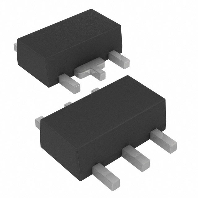


 工商网监
湘ICP备2023018690号
工商网监
湘ICP备2023018690号