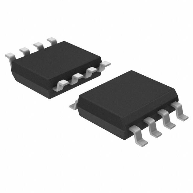
1-1-1 Linear Regulator ICs
SI-3000KS Series Surface-Mount, Low Current Consumption, Low Dropout Voltage Linear Regulator ICs
■Features
• Compact surface-mount package (SOP8) • Output current: 1.0 A • Compatible with low ESR capacitor • Low circuit current at output OFF Iq ≤ 350 µA (IO = 0 A, VC = 2 V) • Low current consumption Iq (OFF) ≤ 1 µA (VC = 0 V) • Low dropout voltage VDIF ≤ 0.6 V (IO = 1 A) • 3 types of output voltages (2.5 V, 3.3 V, and variable type) available • Output ON/OFF control terminal voltage compatible with LS-TTL • Built-in drooping-type-overcurrent and thermal protection circuits
■Absolute Maximum Ratings
Parameter DC Input Voltage Output Control Terminal Voltage DC Output Current Power Dissipation Junction Temperature Storage Temperature Thermal Resistance (Junction to Ambient Air) Thermal resistance (Junction to Lead (pin 7)) Symbol VIN*1 VC IO*1 PD*1, *2 Tj Tstg Ratings 17 VIN 1.0 0.76 –40 to +125 –40 to +125 130 22 Unit V V A W °C °C °C/W °C/W
(Ta=25°C)
θ j-a* θ j-l
*1: VIN (max) and IO (max) are restricted by the relation PD = (VIN - VO) × IO. Please calculate these values referring to the Copper laminate area vs. Power dissipation data as shown hereinafter. *2: When mounted on a glass epoxy board of 1600 mm2 (copper laminate area 2%).
■Applications
• Local power supplies • Battery-driven electronic equipment
■Electrical Characteristics
Ratings Parameter Input Voltage Output Voltage (Reference voltage VADJ for SI-3012KS) Symbol VIN VO (VADJ) Conditions VDIF Dropout Voltage Conditions Conditions Line Regulation Load Regulation Quiescent Circuit Current Circuit Current at Output OFF Temperature Coefficient of Output Voltage Ripple Rejection Overcurrent Protection Starting Current*2 Control Voltage (Output ON)*3 Control Voltage (Output OFF) VC Terminal Control Current (Output ON) Control Current (Output OFF) ∆VOLINE Conditions ∆VOLOAD Conditions Iq Conditions Iq (OFF) Conditions ∆VO/∆Ta Conditions RREJ Conditions IS1 Conditions VC, IH VC, IL IC, IH Conditions IC, IL Conditions –5 0 –5 2.0 0.8 40 VC=2V 0 VC=0V –5 1.2 VIN=3.3V (VO=2.5V) 2.0 0.8 40 VIN=3.3V, VC=0V ± 0.3 Tj=0 to 100°C (VO=2.5V) 55 VIN =3.3V, f=100 to 120HZ (VO=2.5V) 1.2 VIN=3.3V 2.0 IO=0.5A (VO=2.5V) 0.6 IO=1A (VO=2.5V) 10 VIN=3.3 to 8V, IO=10mA (VO=2.5V) 40 VIN=3.3V, IO=0 to 1A (VO=2.5V) 350 VIN=3.3V, IO=0A, VC=2V, R2=24kΩ 1 VIN=3.3V, VC=0V ± 0.3 Tj=0 to 100°C 55 VIN=3.3V, f=100 to 120HZ 1.2 VIN=3.3V, IO=0A, VC=2V 1 VIN=3.3V, IO=0 to 1A 350 VIN=3.3 to 8V, IO=10mA 40 IO=1A 10 SI-3012KS (variable type) min. 2.4 1.24 1.28 VIN=3.3V, IO=10mA 0.3 IO=0.5A 0.6 1.32 typ. max. min.
*1
(Ta=25°C, Vc=2 V unless otherwise specified)
SI-3025KS typ. 2.50 VIN=3.3V, IO=10mA 0.4 IO=0.5A 0.6 IO=1A 15 VIN=5 to 10V, IO=10mA 50 VIN=5V, IO=0 to 1A 350 VIN=5V, IO=0A, VC=2V 1 VIN=5V, VC=0V ± 0.3 Tj =0 to 100°C 55 VIN=5V, f=100 to 120HZ VIN=5V 0.8 40 0 mV mV max. 2.55 min.
*1
SI-3033KS typ. 3.300 VIN=5V, IO=10mA 0.4 max.
Unit V 3.366 V
2.45
3.234
V
µA µA
mV/ °C dB A V
µA µA
*1: Refer to the Dropout Voltage parameter. *2: The Is1 is specified at the 5% drop point of output voltage VO on the condition that VIN = VO + 1 V, and IO = 10 mA. *3: Output is OFF when the output control terminal VC is open. Each input level is equivalent to LS-TTL level. Therefore, the device can be driven directly by LS-TTLs.
14
ICs
�SI-3000KS Series
■External Dimensions (SOP8)
5.1±0.4 1.27 0.4±0.1 0.15+0.1 –0.05
0.5±0.1
(Unit : mm) Pin Assignment q VC w VIN e VO r Sence (ADJ for SI-3012KS) t GND y GND u GND i GND Plastic Mold Package Type Flammability: UL 94V-0 Product Mass: Approx. 0.1 g
8
7
6
5
4.4±0.2
1
2
3
4
0.10 0.4±0.1 0.12 M
■Block Diagram
●SI-3012KS
VIN 2 3 VOUT
0.05±0.05
1.55±0.15
1.5±0.1
0~
0.995max.
10
1.27
°
6.2
●SI-3025KS, SI-3033KS
VIN 2 3 VOUT
4
VC 1 +
4 ADJ TSD 8 7 REF 6 5 GND
VC 1 +
Sense TSD 8 7 REF 6 5 GND
■Typical Connection Diagram
●SI-3012KS
VIN 2
+
●SI-3025KS, SI-3033KS
VO 3 VIN 2 VO 3 CO
R1
CO
CIN
VC GND ADJ 1 4 5 to 8
Load
CIN
sense VC GND 4 1 5 to 8
Load
R2
R2
R1, R2: Output voltage setting resistors The output voltage can be set by connecting R1 and R2 as shown above. The recommended value of R2 is 24 kΩ .
CIN: Input capacitor (22 µF or larger) CO: Output capacitor (22 µF or larger) For SI-3000KS series, Co has to be a low ESR capacitor. When using the electrolytic capacitor, the SI-3000KS series may oscillate at a low temperature.
R1=(VO–VADJ)÷(VADJ/R2)
■Reference Data
Copper Laminate Area vs. Thermal Resistance
140 Area of PC board : 40×40mm
1.2
Copper Laminate Area vs. Power Dissipation
Tj=100°C Area of PC board : 40×40mm Ta=25°C
Thermal resistance θ j-a (°C/W)
120
Power dissipation PD (W)
1
Ta=50°C Ta=80°C
0.8
100
• Obtaining the junction temperature Measure the temperature TL at the lead part of the GND pin (pin 7) with a thermocouple, etc. Then, substitute this value in the following formula to obtain the junction temperature.
0.6 0.4
Tj=PD × θ j–L + TL
( θ j–L = 22°C/W)
80
60
0.2
40 10
100 Copper laminate area (mm2) (GND terminal)
1000
0 10
100 Copper laminate area (mm2) (GND terminal)
1000
ICs
15
�qSI-3000KS Series
sExample of Solder Pattern Design
L
L
b2
e1 l2 e1 B1 L e b e α e e e e *1 B2
Symbol e1 e α β1 β2 L b2 l2
Dimensions (mm) 5.72 1.27± 0.15 0.2 0.2 to 0.5 0.2 0.6 0.76 L+β1+β2
GND pattern b2 8 7 6 5 l2
(Reference value conforming to EIAJ Standard ED-7402-1) *1 The inner frame stage on which a monolithic IC is mounted is directly connected to the GND pins (pins 5 through 8). By expanding the area of the copper connected to the GND pins, the heat radiation can be improved. It is recommended to design the solder pattern by opening the insulation film of the solder patterns of pins 5, 6, 7, and 8, on the wide GND pattern as shown in Figure 1.
e1
1
2
3
4
e
e Figure 1
e
sReference Data
Thermal resistance vs. Copper area
140 Area of PC board : 40×40mm 1.2
Power dissipation vs. Copper area
Tj=100°C Area of PC board : 40×40mm Ta=25°C Ta=50°C Ta=80°C 0.8
Thermal resistance θ j-a (°C/W)
120
Power dissipation PD (W)
1
100
0.6 0.4
80
60 0.2 40 10
100 Copper area (mm2)
1000
0 10
100 Copper area (mm2)
1000
• Calculating junction temperature Measure the temperature TL of the lead of the GND pin (pin 7) by using a thermocouple, and substitute the measured value into the following expression to calculate the junction temperature.
Tj=PD × θj–L + TL
( θj–L = 22°C/W)
�qSI-3000KS Series
sTaping Specifications
Carrier tape Surface resistance of embossed tape: 100 k Ω maximum (among 10 pockets)
Leader Vacant seal section Trailer IC compartments Vacant seal section Cover tape
(Unit : mm)
160 to 240mm (About 25 pockets)
1,000PCS (1,000 pockets)
160 to 240mm (About 25 pockets) 400 to 600mm
4
2
8
φ1.55
Tape draw-out direction
t=3 5.5 12 5.75 (4.75) 5.55
7.0
φ2
2.1
6.7
Reel: Number of packed products: 1000
Hole
Hole B
1.5
60
°
60
°
Hole
Hole
φ13±0.2
φ 60 φ 180
φ R2 3 2
Hole 13±0.3 15.4±1.0
Hole
φ1
0
Hole
Hole
Expanded view of center
2
5
φ1 3
.5 10
Hole
4
Hole
5
30°
11.9
Hole
10
Hole
φ3
2 R2
φ
60 °
3
° 60
�qSI-3000KS Series
sTypical Characteristics Examples of SI-3012KS and SI-3025KS
(Ta=25°C) *Vout=2.5 V for SI-3012KS (RS=24 kΩ)
Dropout voltage
1
Rise characteristics
3
Line regulation
2.54 2.52
0.8
2.50 Dropout voltage V
0.6
Output voltage V
Output voltage V
2 IO=0 to 1A 0.25A step 1
2.48 2.46 2.44 2.42 2.40 0 IO=0 to 1A 0.25A step
0.4
0.2
0
0.2
0.4 0.6 Output current A
0.8
1
0
1
2 Input voltage V
3
4
2
4 6 Input voltage V
8
10
Load regulation
2.52
Overcurrent protection characteristics
3
Input voltage vs. Quiescent current
600 IO=0A VC=2V
2.50 2 VIN=3.3V 4V 5V 6V
Quiescent Current µ A
500
Output voltage V
2.48 VIN=3.3V 4V 5V 6V 8V
Output voltage V
400
2.46
300
2.44
1
200
2.42
100
2.40 0
0.2
0.4 0.6 Output current A
0.8
1
0
0.2
0.4
0.6 0.8 1 1.2 Output current A
1.4
1.6
0
2
4
6 8 10 12 Input voltage V
14
16
18
Circuit current
60
Control terminal voltage vs. Output voltage
3
Control terminal voltage vs. Control terminal current
30
25
GND current mA
IO=1A
Output voltage V
40
2
IO=0A
Control terminal current µ A
2
20
15
0.75A 20 0.5A 0.25A 0 2 4 Input voltage V 6 0A 8
1
10 5
0
0.5 1 1.5 Control ternimal voltage V
0
1 2 3 Control terminal voltage V
4
�qSI-3000KS Series
sTypical Characteristics Examples of SI-3033KS
(Ta=25°C)
Dropout voltage
1
Rise characteristics
4
Line regulation
3.34 3.32
0.8
3
Output voltage V
3.30
Dropout voltage V
0.6
Output voltage V
3.28 3.26 3.24
2
0.4
IO=0 to 1A 0.25A step
0.2
1
3.22 3.20 0
IO=0 to 1A 0.25A step
0
0.2
0.4 0.6 Output current A
0.8
1
0
1
2 Input voltage V
3
4
2
4 6 8 Input voltage V
10
12
Load regulation
3.34 3.32
Overcurrent protection characteristics
4
Input voltage vs. Quiescent current
600 IO=0A VC=2V
500
3 Quiescent Current µ A 1.4 1.6
Output voltage V
3.30
Output voltage V
400
3.28 3.26 3.24 3.22 3.20 0 VIN=4V 5V 6V 8V
2
VIN=4V 5V 6V
300
200
1
100
0.2
0.4 0.6 Output current A
0.8
1
0
0.2
0.4
0.6 0.8 1 1.2 Output current A
0
2
4
6 8 10 12 Input voltage V
14
16
18
Circuit current
60
Control terminal voltage vs. Output voltage
4
Control terminal voltage vs. Control terminal current
30
25
3
GND current mA
Output voltage V
40 IO=1A
Control terminal current µ A 2
20
IO=0A 2
15
0.75A
20
10
0A
0.5A 0.25A
0 2 4 Input voltage V 6 8
1
5
0
0.5 1 1.5 Control terminal voltage V
0
1 2 3 Control terminal voltage V
4
�