SI-8001FDL DC-to-DC Step-Down Converter
Features and Benefits
▪ 3.5 A output current supplied in a small, surface mount power package ▪ High efficiency: 83% at VIN = 15 V, IO = 2.0 A,VO = 5 V ▪ Requires only six external components ▪ Oscillation circuit built-in (frequency 300 kHz typical) ▪ Constant-current mode overcurrent protection circuit and overtemperature protection circuit built-in ▪ Output-on state at low level ▪ Low current consumption during output-off state
Description
The SI-8001FDL DC voltage regulator is a DC-to-DC buck convertor that attains an oscillation frequency of 300 kHz, and has an integrated miniaturized choke coil, allowing it to serve as a small, high efficiency power supply in a compact TO263 package. The internal switching regulator function provides high efficiency switching regulation without any need for adjustment. The device requires only six external support components. Optional on/off control can be performed using a transistor. The SI-8001FDL includes overcurrent and overtemperature protection circuits. Applications include: ▪ DVD recorder ▪ FPD TV ▪ Telecommunications equipment ▪ Office automation equipment, such as printers ▪ On-board local power supply ▪ Output voltage regulator for second stage of SMPS (switched mode power supply)
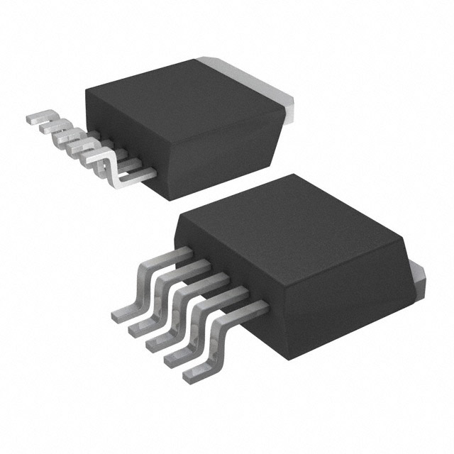
Package: TO263-5
Not to scale
Functional Block Diagram
VIN 1 IN C1 PReg Overcurrent Protection Latch and Driver SW 2 L1 Di SPB-G56S (Sanken) VOUT C2
Reset 5 VC On/Off Osc Comparator
R1
Overtemperature Protection Error Amplifier
ADJ
4
R2 Reference Voltage
GND 3
27469.064-I
�SI-8001FDL
DC-to-DC Step-Down Converter
Selection Guide
Part Number SI-8001FDL-TL Output Voltage Adjustable Range (V) 0.8 to 24 Efficiency, Typ. (%) 83 Input Voltage, Max. (V) 40 Output Current, Max. (A) 3.5 Packing 800 pieces per reel
Absolute Maximum Ratings
Characteristic DC Input Voltage VC Pin Control Voltage Power Dissipation Junction Temperature Storage Temperature Thermal Resistance (junction-to-case) Thermal Resistance (junction-to-ambient air) Symbol VIN VC PD TJ Tstg RθJC RθJA Mounted on 40 mm × 40 mm exposed copper area on 40 mm × 40 mm glass-epoxy PCB. Mounted on 40 mm × 40 mm exposed copper area on 40 mm × 40 mm glass-epoxy PCB. Mounted on 40 mm × 40 mm exposed copper area on 40 mm × 40 mm glass-epoxy PCB; limited by internal overtemperature protection. Internal overtemperature protection circuit may enable when TJ ≥ 130°C. During product operation, recommended TJ ≤ 125°C. Remarks Rating 43 VIN 3 –40 to 150 –40 to 150 3 33.3 Units V V W °C °C °C/W °C/W
Recommended Operating Conditions*
Characteristic DC Input Voltage Range DC Output Voltage Range DC Output Current Range Operating Junction Temperature Range Operating Temperature Range Symbol VIN VO IO TJOP TOP To be used within the allowable package power dissipation characteristics (refer to Power Dissipation chart). VIN ≥ VO + 3 V; to be used within the allowable package power dissipation characteristics (refer to Power Dissipation chart). Remarks VIN (min) is the greater of 4.5 V or VO+3 V. Min. See remarks 0.8 0 –30 –30 Max. 40 24 3.5 100 85 Units V V A °C °C
*Required for normal device functioning according to Electrical Characteristics table.
All performance characteristics given are typical values for circuit or system baseline design only and are at the nominal operating voltage and an ambient temperature, TA, of 25°C, unless otherwise stated.
Sanken Electric Co., Ltd. 3-6-3 Kitano, Niiza-shi, Saitama-ken 352-8666, Japan Phone:+81-48-472-1111 http://www.sanken-ele.co.jp
2
�SI-8001FDL
DC-to-DC Step-Down Converter
ELECTRICAL CHARACTERISTICS1, valid at TA = 25°C, VO = 5 V (adjusted), R1 = 4.2 kΩ, R1 = 0.8 kΩ
Characteristic Reference Voltage Reference Voltage Temperature Coefficient Efficiency2 Operating Frequency Line Regulation Load Regulation Overcurrent Protection Threshold Current VC Terminal Control Voltage (On) VC Terminal Control Voltage (Off) VC Terminal Control Current (On) Quiescent Current 1 Quiescent Current 2
1Using
Symbol VADJ ∆VADJ /∆T η fO VLine VLoad IS VC(IH) VC(IL) IC(IH) Iq Iq(off) VC = 2 V
Test Conditions1 VIN = 15 V, IO = 0.2 A VIN = 15 V, IO = 0.2 A, TC = 0 to 100 °C VIN = 15 V, IO = 2 A VIN = 15 V, IO = 2 A VIN = 10 to 30 V, IO = 2 A VIN = 15 V, IO = 0.2 to 3.5 A VIN = 15 V
Min. 0.784 – – 270 – – 3.6 – 2 – – –
Typ. 0.800 ±0.1 83 300 – – – – – 6 6 30
Max. 0.816 – – 330 80 50 – 0.8 – 100 – 200
Units V mV/°C % kHz mV mV A V V μA mA μA
VIN = 15 V, IO = 0 A VIN = 15 V, VC = 0 V
circuit shown in Typical Application Circuit diagram. 2Efficiency is calculated as: η(%) = ([V × I ] × [V × I ]) × 100. O O IN IN
Pin-out Diagram
1 2 3 4 5
Terminal List Table
Name IN SW GND ADJ VC Number 1 2 3 4 5 Supply voltage Regulated supply output Ground terminal Terminal for resistor bridge feedback If the VC terminal is left open, output will be in the on state. Because the input level is equivalent to LS-TTL, direct drive by LS-TTL is possible. Function
VC Pin Control
Input Current versus Input Voltage IO = 0 A, TA = 25°C, R1 = 4.2 kΩ, R2 = 0.8 kΩ
40
30 IC (μA)
20
10
0 0 10 20 VC (V) 30 40
Sanken Electric Co., Ltd. 3-6-3 Kitano, Niiza-shi, Saitama-ken 352-8666, Japan Phone:+81-48-472-1111 http://www.sanken-ele.co.jp
3
�SI-8001FDL
DC-to-DC Step-Down Converter
Performance Characteristics
At TA = 25°C, VO = 5 V Adjusted, R1 = 4.2 kΩ, R2 = 0.8 kΩ
90 85
6.00 5.00
8V 15 V 20 V 30 V VIN IO 0A 0.5 A
80
4.00 VO (V)
Efficiency versus Output Current VO= 3.3 V
η (%)
1A 2A 3.5 A
75 70 65 60
40 V
Low Voltage Behavior: Output Voltage versus Supply Voltage
3.00 2.00 1.00 0
0
0.5
1.0
1.5 2.0 IO (A)
2.5
3.0
3.5
0
1
2
3
4 5 VIN (V)
6
7
8
90
5.10
8V 15 V
5.08
VIN
85 80
5.06 5.04
VIN 40 V 30 V 15 V 10 V 8V
Efficiency versus Output Current VO= 5.0 V
75 70
20 V 30 V 40 V
Load Regulation: 5.02 Output Voltage 5.00 versus Output Current 4.98
VO (V)
η (%)
4.96 4.94 4.92 4.90
0 0.5 1.0 1.5 2.0 IO (A) 2.5 3.0 3.5
65 60
0 10
1
2 IO (A)
3
100 95
15V
90
20 V
VIN
8 6 4 2 0
Efficiency versus Output Current VO= 12.0 V
85
30 V
80
Quiescent Current versus Supply Voltage IO = 0 A VC = 0 V
η (%)
40 V
75 70 0 0.5 1.0 1.5 2.0 IO (A) 2.5 3.0 3.5
Iq (mA)
0
10
20 VIN (V)
30
40
50
6 5
8V
40
Behavior at Turn-Off: Quiescent Current versus Input Voltage IO = 0 A VC = 2 V
IQ (μA)
30
20
Overcurrent Protection: Output Voltage versus Output Current
4
VO (V)
VIN
15 V 30 V
3 2 1 0
40 V
10
0 0 10 20 VIN (V) 30 40
0
1
2
IO (A)
3
4
5
Sanken Electric Co., Ltd. 3-6-3 Kitano, Niiza-shi, Saitama-ken 352-8666, Japan Phone:+81-48-472-1111 http://www.sanken-ele.co.jp
4
�SI-8001FDL
DC-to-DC Step-Down Converter
Thermal Performance Characteristics
The application must be designed to ensure that the TJ(max) of the device is not exceeded during operation. To do so, it is necessary to determine values for maximum power dissipation, PD(max), and ambient temperature, TA(max). The relationships of TJ, PD, TA, and case temperature, TC, are as shown in the following formulas: PD = TJ – TC RθJC
Power Dissipation versus Ambient Temperature
TJ(max) = 125°C; Mounted on glass-epoxy PCB (40 mm × 40 mm), with varying exposed copper areas
3.5
Cu Area: 1600 mm2 RθJA = 33.3°C/W
3.0
Cu Area: 800 mm2 RθJA = 37°C/W
and
PD =
TJ – TA RθJA
.
2.5
PD can be calculated from input values:
⎛ 100 ⎞ ⎛V − 1⎟ − VF ⋅ I O ⎜1 − O PD = VO ⋅ I O ⎜ ⎜ ⎟ ⎜V IN ⎝x ⎠ ⎝
where: VO is output voltage in V, VIN is input supply voltage in V, IO is output current in A,
⎞ ⎟ ⎟ ⎠
2.0 PD (W)
Cu Area: 400 mm2 RθJA = 44°C/W
1.5
Cu Area: 100 mm2 RθJA = 53°C/W
1.0
ηx is IC efficiency in percent (varies with VIN and IO; refer to efficiency performance curves for value), and VF is forward voltage for the input diode, Di. In these tests, the Sanken SPB-G56S was used, at 0.4 V. For application design, obtain thermal data from the datasheet for the diode. PD is substantially affected by the heat conductance properties of the application, in particular any exposed copper area on the PCB where the device is mounted. The relationships of PD, TA, and copper area is represented in the Power Dissipation chart. RθJA for a given copper area can be determined form the Device Thermal Resistance chart. This can be substituted into the formula above to determine the TJ (max) allowable in the application. Generally, more than 10% to 20% derating is required. Because the heat dissipation capacity of the copper area depends substantively on how it is used in the actual application, thermal characteristics of the application must be confirmed by testing. TC is determined by connecting a thermocouple to the device as shown here:
0.5
0 –25 0 25 50 TA (°C) 75 100 125
Device Thermal Resistance versus Exposed Copper Area on PCB
55
RθJA(°C/W) Glass-epoxy PCB, 40 mm × 40 mm
50 45 40 35 30
0 200 400 600 800 1000 1200 1400 1600 1800
Copper Area (mm2)
6
OTP On
5
Overtemperature Protection: Output Voltage versus Junction Temperature
VIN = 15 V, IO = 10 mA
4 VO (V) 3 2 1
Thermocouple mount at tab center
And analyzing the results using the following formula: TJ = PD × RθJC + TC , for this device, RθJC is 3 °C/W.
Sanken Electric Co., Ltd. 3-6-3 Kitano, Niiza-shi, Saitama-ken 352-8666, Japan Phone:+81-48-472-1111 http://www.sanken-ele.co.jp
OTP Off
0 0 20 40 60 80 100 TJ (°C) 120 140 160 180
5
�SI-8001FDL
DC-to-DC Step-Down Converter
Component Selection
Diode Di A Schottky-barrier diode must be used for Di. If other diode types are used, such as fast recovery diodes, the IC may be destroyed because of the reverse voltage applied by the recovery voltage or ON voltage. Choke Coil L1 If the winding resistance of the choke coil is too high, the efficiency may be reduced below rating. Because the overcurrent protection start current is approximately 4.2 A, attention must be paid to the heating of the choke coil by magnetic saturation due to overload or short-circuited load. Capacitors C1 and C2 Because for SMPS, large ripple currents flow across C1 and C2, capacitors with high frequency and low impedance must be used. If the impedance of C2 is too high,
the switching waveform may not be normal at low temperatures. Do not use either OS or tantalum types of capacitors for C2, because the extremely low ESR causes an abnormal oscillation. The device is stabilized, and for proper operation, C1 must be located close to the device (see layout diagram, below). Resistor Bridge R1 and R2 comprise the resistor bridge for the output voltage, VO, and are calculated as follows: (V − V ) (V − 0.8) (Ω) , and R2 = VADJ = 0.8 = 0.8 (k Ω ) R1 = O ADJ = O −3 −3
IADJ 1 × 10 IADJ 1 × 10
IADJ should always be set to 1 mA. Note that R2 should always be present to ensure stable operation, even if VO, is set to 0.8 V (that is, even if there is no R1). VO should be at least VIN + 8%.
Typical Application Diagram
VIN L1 VO
1 IN SW SI-8001FDL VC GND 3 5 C1 ADJ
2
Component C1 C2 Di L1
Rating 470 μF 680 μF SPB-G56S (Sanken) 47 μH
4 Di
R1 IADJ R2 C2 GND
GND
Recommended PCB Layout
Recommended Solder Pad Layout
11±0.2
9±0.2
Vc
6.8±0.1
9±0.1
Di R1
3.7±0.05
R2
4±0.1 1±0.05
All external components should be mounted as close as possible to the SI-8001FDL. The ground of all components should be connected at one point near GND pin (pin 3).
1.7±0.1 (mm)
Sanken Electric Co., Ltd. 3-6-3 Kitano, Niiza-shi, Saitama-ken 352-8666, Japan Phone:+81-48-472-1111 http://www.sanken-ele.co.jp
6
�SI-8001FDL
DC-to-DC Step-Down Converter
PACKAGE OUTLINE DRAWING
2.20 ±0.20 9.90 ±0.20 (0.75) (0.40) + (6.80) (R0.45) 4.50 ±0.20 3XR0.30
15º
(8.00) (4.40)
1.30 –0.05
+0.10
(4.60)
Ø1.5 ±0.20
XXXXXXXX
XXXXXXXX XXXXXXXX
3º
+
15.30 ±0.30
Branding
XXXXXXXX
9.20 ±0.20
3XR0.30 0.10 ±0.15
2.00 ±0.10
3º
(0.75)
0.88 ±0.10 0.80 ±0.10
4.90 ±0.20
3º
2.40 ±0.20
(R0.30) (0.50)
6º 0º
4×P1.70 ±0.25
3º
2XR0.30
1
2
3 4 10.00 ±0.02
5
Branding codes (exact appearance at manufacturer discretion): 1st line: SK 2nd line, lot: YMW X Where: Y is the last digit of the year of manufacture M is the month (1 to 9, O, N, D) W is the week of the month (1 to 5) X is the device subtype suffix number 3rd line, type: 8001FDL
Dimensions do not include mold protrusion Heastsink side flash: 0.8 mm maximum Dimensions in millimeters
RoHS directive compliant Device pins lead (Pb) free
2.54 ±0.30
Sanken Electric Co., Ltd. 3-6-3 Kitano, Niiza-shi, Saitama-ken 352-8666, Japan Phone:+81-48-472-1111 http://www.sanken-ele.co.jp
7
�SI-8001FDL
DC-to-DC Step-Down Converter
TAPE AND REEL SPECIFICATION
Ø1.5
+0.1 –0.0
2.0 ±0.10 B
1.75 ±0.10
4.0 ±0.10
0.4 ±0.05
11.5 ±0.05
24.3 ±0.03
A
A 16.0 10.6 B
Ø1.5 MIN 3.9 4.9
View A-A
15.7 View B-B
Material: Conductive polysterene Camber < 1 mm over of tape Camber < 1 mm over 100 mm length100 length of tape Pocket inner widths measured 0.3 of cavity Pocket inner widths measured 0.3 mm above floormm above floor of pocket
Material: conductive polysterene
Pocket position relative to sprocket hole measured to true position of pocket 10 sprocket hole pitch cumulative ±0.2 mm Pocket center and pocket hole center ±0.3 mm Surface resistivity < 107 Ω / cm2
Sanken Electric Co., Ltd. 3-6-3 Kitano, Niiza-shi, Saitama-ken 352-8666, Japan Phone:+81-48-472-1111 http://www.sanken-ele.co.jp
8
�SI-8001FDL
DC-to-DC Step-Down Converter
PACKING SPECIFICATION
Inner Carton 800 pieces per reel 2 reels per carton
341 65
344
Outer Carton 3 inner cartons per outer carton
450 230
Dimensions in mm
350
Sanken Electric Co., Ltd. 3-6-3 Kitano, Niiza-shi, Saitama-ken 352-8666, Japan Phone:+81-48-472-1111 http://www.sanken-ele.co.jp
9
�SI-8001FDL
DC-to-DC Step-Down Converter
WARNING — These devices are designed to be operated at lethal voltages and energy levels. Circuit designs that embody these components must conform with applicable safety requirements. Precautions must be taken to prevent accidental contact with power-line potentials. Do not connect grounded test equipment. The use of an isolation transformer is recommended during circuit development and breadboarding.
Cautions for Use • Operation of the product in parallel to increase current is not permitted. • Although the product has an internal overtemperature protection circuit, that is intended only to protect the product from temporary excess heating due to overloads. Long-term reliability cannot be guaranteed when the product is operated under continuous overload conditions. Because reliability can be affected adversely by improper storage environments and handling methods, please observe the following cautions. Cautions for Storage • Ensure that storage conditions comply with the standard temperature (5°C to 35°C) and the standard relative humidity (around 40 to 75%); avoid storage locations that experience extreme changes in temperature or humidity. • Avoid locations where dust or harmful gases are present and avoid direct sunlight. • Reinspect for rust on leads and solderability of products that have been stored for a long time. Cautions for Testing and Handling When tests are carried out during inspection testing and other standard test periods, protect the products from power surges from the testing device, shorts between adjacent products, and shorts to the heatsink. Electrostatic Discharge • When handling the products, operator must be grounded. Grounded wrist straps worn should have at least 1 MΩ of resistance to ground to prevent shock hazard. • Workbenches where the products are handled should be grounded and be provided with conductive table and floor mats. • When using measuring equipment such as a curve tracer, the equipment should be grounded. • When soldering the products, the head of soldering irons or the
solder bath must be grounded in other to prevent leak voltages generated by them from being applied to the products. • The products should always be stored and transported in our shipping containers or conductive containers, or be wrapped in aluminum foil.
Soldering • When manually soldering the products, please be sure to minimize the working time, within the following limits: Soldering Iron Temperature (°C) 380±10 Time (s) 3 (once only)
•
Reflow soldering can be performed a maximum of twice, using the following recommended profile:
250 230 Temperature (°C) 250°C Maximum
180 150 90 ±30s Time 30 ±10s
Sanken Electric Co., Ltd. 3-6-3 Kitano, Niiza-shi, Saitama-ken 352-8666, Japan Phone:+81-48-472-1111 http://www.sanken-ele.co.jp
10
�SI-8001FDL
DC-to-DC Step-Down Converter
Application and operation examples described in this document are quoted for the sole purpose of reference only, for the use of the products herein, and Sanken can assume no responsibility for any infringement of industrial property rights, intellectual property rights, or any other rights of Sanken or any third party which may result from its use. When using the products herein, the applicability and suitability of such products for an intended purpose or object shall be reviewed at the user’s responsibility. Although Sanken undertakes to enhance the quality and reliability of its products, the occurrence of failure and defect of semiconductor products at a certain rate is inevitable. Users of Sanken products are requested to take, at their own risk, preventative measures including safety design of the equipment or systems against any possible injury, death, fires or damages to the society due to device failure or malfunction. Sanken products listed in this document are designed and intended for the use as components in general purpose electronic equipment or apparatus (home appliances, office equipment, telecommunication equipment measuring equipment, etc.). Before placing an order, the user’s written consent to the specifications is requested. When considering the use of Sanken products in the applications where higher reliability is required (transportation equipment and its control systems, traffic signal control systems or equipment, fire/crime alarm systems, various safety devices, etc.), please contact your nearest Sanken sales representative to discuss and obtain written confirmation of your specifications. The use of Sanken products without the written consent of Sanken in the applications where extremely high reliability is required (aerospace equipment, nuclear power control systems, life support systems, etc.) is strictly prohibited. Anti radioactive ray design is not considered for the products listed herein. If there is any discrepancy between English and Japanese versions of this datasheet, the Japanese version should take precedence over the English one. Please accept in advance that the content of this datasheet is subject to change without notice for the purpose of such as improvement of the product.
Copyright © 2007 Sanken Electric Co., Ltd.
This datasheet is based on Sanken datasheet SSJ-03151
Sanken Electric Co., Ltd. 3-6-3 Kitano, Niiza-shi, Saitama-ken 352-8666, Japan Phone:+81-48-472-1111 http://www.sanken-ele.co.jp
11
�DC-to-DC Step-Down Converter
SI-8001FDL
June, 2007
Asia Pacific
China
Sanken Electric Hong Kong Co., Ltd. Suite 1026 Ocean Centre, Canton Road, Tsimshatsui, Kowloon, Hong Kong Tel: 852-2735-5262 Fax: 852-2735-5494 Sanken Electric (Shanghai) Co., Ltd. Room3202, Maxdo Centre, Xingyi Road 8, Changning district, Shanghai, China Tel: 86-21-5208-1177 Fax: 86-21-5208-1757 Taiwan Sanken Electric Co., Ltd. Room 1801, 18th Floor, 88 Jung Shiau East Road, Sec. 2, Taipei 100, Taiwan R.O.C. Tel: 886-2-2356-8161 Fax: 886-2-2356-8261
India
Saket Devices Pvt. Ltd. Office No.13, First Floor, Bandal - Dhankude Plaza, Near PMT Depot, Paud Road, Kothrud, Pune - 411 038, India Tel: 91-20-5621-2340 91-20-2528-5449 Fax: 91-20-2528-5459
Japan
Sanken Electric Co., Ltd. Overseas Sales Headquaters Metropolitan Plaza Bldg. 1-11-1 Nishi-Ikebukuro, Toshima-ku, Tokyo 171-0021, Japan Tel: 81-3-3986-6164 Fax: 81-3-3986-8637
Korea
Sanken Electric Korea Co., Ltd. Mirae Asset Life Bldg. 6F, 168 Kongduk-dong, Mapo-ku, Seoul, 121-705, Korea Tel: 82-2-714-3700 Fax: 82-2-3272-2145
Singapore
Sanken Electric Singapore Pte. Ltd. 150 Beach Road, #14-03 The Gateway West, Singapore 189720 Tel: 65-6291-4755 Fax: 65-6297-1744
Sanken Electric Co., Ltd.
I02-006EA-070628
�DC-to-DC Step-Down Converter
SI-8001FDL
Europe
United Kingdom
Sanken Power Systems (UK) Limited Pencoed Technology Park, Pencoed, Bridgend CF35 5HY. UK Tel: 44-1656-869-100 Fax: 44-1656-869-162
June, 2007
North America
United States
Allegro MicroSystems, Inc. 115 Northeast Cutoff, Worcester, Massachusetts 01606, U.S.A. Tel: 1-508-853-5000 Fax: 1-508-853-3353 Allegro MicroSystems, Inc. (Southern California) 14 Hughes Street, Suite B105, Irvine, CA 92618 Tel: 1-949-460-2003 Fax: 1-949-460-7837
Sanken Electric Co., Ltd.
I02-006EA-070628
�