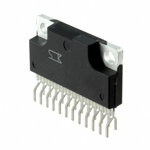
SLA6845MZ
High Voltage 3-Phase Motor Driver
Features and Benefits
▪
▪
▪
▪
▪
▪
▪
▪
▪
▪
▪
Description
Built-in pre-drive IC
IGBT power element
CMOS compatible input (3.3 to 5 V)
High-side gate driver using bootstrap circuit or floating
power supply
Integrated Fast Recovery Diode (FRD) as freewheeling
diode for each IGBT
Built-in protection circuit for controlling power supply
voltage drop
Built-in overtemperature detection circuit (TD)
3-shunt configuration
Output of fault signal during operation of protection
circuit
Output current 3 A
Small SIP (SLA 24-pin)
The SLA6845MZ inverter power module (IPM) device provides
a robust, highly-integrated solution for optimally controlling
3-phase motor power inverter systems and variable speed
control systems used in energy-conserving designs to drive
motors of residential and commercial appliances. These ICs
take 230 VAC input voltage, and 3 A (continuous) output
current. They can withstand voltages of up to 600 V (IGBT
breakdown voltage).
The SLA6840M power package includes an IC with all of
the necessary power elements (six IGBTs), pre-driver ICs
(two), and freewheeling diodes (six), needed to configure the
main circuit of an inverter. This enables the main circuit of
the inverter to be configured with fewer external components
than traditional designs.
Applications include residential white goods (home
applications) and commercial appliance motor control:
• Air conditioner fan
• Refrigerator compressor
• Dishwasher pump
Package: Power SIP
Leadform
2171
Leadform
2178
Leadform
2175
Not to scale
Functional Block Diagram
VB 1
VB 2
VB3
VBB 1
VCC1
VBB 2
UVLO
HIN1
HIN2
HIN3
Input
Logic
UVLO
UVLO
UVLO
High Side
Level Shift Driver
COM1
VCC2
VREG
LIN1
LIN2
LIN3
7.5 V
Reg.
UVLO
Input
Logic
COM2
FO
Figure 1. Driver block diagram.
SLA6845MZ-DS
Overtemperature
Detection
U
V
W1
W2
Low Side
Driver
LS3
LS2
LS1
�SLA6845MZ
High Voltage 3-Phase Motor Driver
Selection Guide
Output Current
Part Number
Packing
IGBT Breakdown
Voltage, VCES(min)
(V)
IGBT Saturation
Voltage, VCE(sat)(typ)
(V)
Continuous, IO(max)
(A)
Pulsed, IOP (max)
(A)
SLA6845MZ
18 pieces per tube
600
1.75
3
6
Absolute Maximum Ratings, valid at TA = 25°C
Characteristic
Symbol
Main Supply Voltage
VBB
Main Supply Voltage (Peak)
VBB(surge)
Remarks
Rating
Unit
Maximum voltage that can be applied between VBB and LSx
continuously
450
V
Maximum voltage allowed between VBB and LSx, including transient
switching noise. If surge voltages reach this rating, the snubber circuit
should be improved so the voltage does not exceed this level.
500
V
IGBT Breakdown Voltage
VCES
600
V
Logic Supply Voltage
VCC
Between VCC and COM
20
V
Bootstrap Voltage
VBS
Between VB and HS (U,V, and W phases)
20
V
IO
TC = 25°C
3
A
Output Current, Pulsed
IOP
PW ≤ 100 μs
Output Current for Regulator
IREG
Input Voltage
VIN
Allowable Power Dissipation
PD
Output Current, Continuous
Thermal Resistance (Junction to Case)
TC = 25°C, all elements operating
6
A
35
mA
–0.5 to 7
V
32
W
RθJC(I)
All elements operating (IGBT)
3.8
°C/W
RθJC(F)
All elements operating (FRD)
4.2
°C/W
Thermal Resistance (Junction to Ambient)
RθJA
25
°C/W
Case Operating Temperature
TCOP
All elements operating (IGBT and FRD)
–20 to 100
°C
Junction Temperature (IGBT)
TJ
150
°C
Storage Temperature
Tstg
–40 to 150
°C
Max.
Units
Recommended Operating Conditions
Characteristic
Symbol
Remarks
Main Supply Voltage
VBB
Between VBB and LS, IBB ≤ 2 A
Logic Supply Voltage
VCC
Between VCC and COM
RS
Min.
Typ.
–
300
450
V
13.5
–
16.5
V
LS1, LS2, LS3 to COM2
0.3
–
–
Ω
Dead Time
tdead
Between LS1, LS2, LS3 and COM
1.5
–
–
μs
Overcurrent Protection (OCP)
Response Time
tOCP
No built-in OCP. If OCP required, implement using
an external circuit. Measure tOCP from overcurrent
occurrence to shutdown command received on
corresponding HINx or LINx terminal.
–
–
2.0
μs
Snubber Capacitor
CS
Between VCC and COM. Use properly-rated film
capacitor for voltage surge suppression.
0.01
–
0.1
μF
Junction Temperature
TJ
–
–
125
°C
Shunt Resistor
All performance characteristics given are typical values for circuit or
system baseline design only and are at the nominal operating voltage and
an ambient temperature, TA, of 25°C, unless otherwise stated.
Allegro MicroSystems, Inc.
115 Northeast Cutoff, Box 15036
Worcester, Massachusetts 01615-0036 (508) 853-5000
www.allegromicro.com
2
�SLA6845MZ
High Voltage 3-Phase Motor Driver
Typical Application Diagram
DBOOT RBOOT
2
3
4
VB1
VB2
VB3
SLA6845MZ
11
10
5
VCC1
HO1
HVIC
HS1
1
HO2
9
8
7
6
HS2
13
M
HIN1
HIN2
HIN3
HO3
COM1
HS3
Cs
12
14
23
VCC2
LVIC
Controller
LO1
24
20
19
18
16
LIN1
LO2
17
LIN2
LIN3
LO3
VREG
15
CC
22
21
FO
COM2
RS
15V
NOTE:
▪ All of the input pins are connected to GND with internal pull-down resistors rated at 100 kΩ, however, an external pull-down
resistor may be required to secure stable condition of the inputs if high impedance conditions are applied to them.
▪ The external electrolytic capacitors should be placed as close to the IC as possible, in order to avoid malfunctions from
external noise interference. Put a ceramic capacitor in parallel with the electrolytic capacitor if further reduction of noise
susceptibility is necessary.
Allegro MicroSystems, Inc.
115 Northeast Cutoff, Box 15036
Worcester, Massachusetts 01615-0036 (508) 853-5000
www.allegromicro.com
3
�SLA6845MZ
High Voltage 3-Phase Motor Driver
ELECTRICAL CHARACTERISTICS, valid at TA=25°C, unless otherwise noted
Characteristics
Logic Supply Voltage
Logic Supply Current
Input Voltage
Input Voltage Hysteresis
Input Current
Symbol
Between VCC and COM
FO Terminal Output Voltage
Overtemperature Detection Activating
and Releasing Temperature
Units
16.5
V
–
4
6
mA
VCC = 15 V, output on
–
2.0
2.5
V
VIL
VCC = 15 V, output off
1.0
1.5
–
V
–
0.5
–
V
VIhys
VCC = 15 V
IIH
High side, VCC = 15 V, VIN = 5 V
–
50
100
μA
IIL
Low side, VCC = 15 V, VIN = 0 V
–
–
2
μA
9.0
10.0
11.0
V
9.5
10.5
11.5
V
–
0.5
–
V
VUVHhys
VUVLL
VUVLhys
LS Negative Surge
Max
15
VCC = 15 V, VIN = 5 V
VUVLH
Voltage2
Typ
ICC
VUVHL
–VO for Output Voltage1
Min
13.5
VIH
VUVHH
Undervoltage Lockout
Conditions
VCC
High side, between VB and U, V, or W
High side, hysteresis
Low side, between VCC and COM
10.0
11.0
12.0
V
10.5
11.5
12.5
V
Low side, hysteresis
–
0.5
–
V
–VO
Between U, V, or W and COM
–5
–
–
V
VLS
Between LS1, LS2, or LS3 and COM
–5
–
5
V
VFOL
VCC = 15 V, IFO = –1 mA
0
–
1.0
V
VFOH
VCC = 15 V, IFO = –1.6 mA
TTDH
TTDL
VCC = 15 V, no heatsink, IREG = 0 mA
TTDhys
4.0
–
5.5
V
135
150
165
°C
105
120
135
°C
–
30
–
°C
V
Output Voltage for Regulator
VREG
IREG = 0 to 35 mA
6.75
7.5
8.25
IGBT Breakdown Voltage
VCES
VCC = 15 V, IC = 1 mA, VIN = 0 V
600
–
–
V
IGBT Leakage Current
ICES
VCC = 15 V, VCE = 600 V, VIN = 0 V
–
–
1
mA
IGBT Saturation Voltage
VCE(sat)
VCC = 15 V, IC = 3 A, VIN = 5 V
–
1.75
2.1
V
Diode Forward Voltage
VF
VCC = 15 V, IF = 3 A, VIN = 0 V
–
1.65
2.0
V
trr
IF = 3 A, di / dt = 100 A/μs
Diode Recovery Time
Switching Time, High Side
–
50
–
ns
tdH(on)
–
315
–
ns
trH
–
50
–
ns
tdH(off)
–
375
–
ns
–
165
–
ns
–
325
–
ns
trL
–
60
–
ns
tdL(off)
–
400
–
ns
tfL
–
165
–
ns
tfH
tdL(on)
Switching Time, Low Side
1Indicates
2Indicates
VBB = 300 V, VCC = 15 V, IC = 3 A, 0 V ≤ VIN ≤ 5 V,
inductive load
normal operating range for the high-side driver IC.
the allowable range assuming any transient surge


 工商网监
湘ICP备2023018690号
工商网监
湘ICP备2023018690号
