Ordering number : ENA0553B
2SK4085LS
SANYO Semiconductors
DATA SHEET
N-Channel Silicon MOSFET
2SK4085LS
Features
• • • •
General-Purpose Switching Device Applications
Low ON-resistance, low input capacitance, ultrahigh-speed switching. High reliability (Adoption of HVP process). Attachment workability is good by Mica-less package. Avalanche resistance guarantee.
Specifications
Absolute Maximum Ratings at Ta=25°C
Parameter Drain-to-Source Voltage Gate-to-Source Voltage Drain Current (DC) Drain Current (Pulse) Allowable Power Dissipation Channel Temperature Storage Temperature Avalanche Energy (Single Pulse) *4 Avalanche Current *5 Symbol VDSS VGSS IDc*1 IDpack*2 IDP PD Tch Tstg EAS IAV Limited only by maximum temperature Tc=25°C (SANYO’s ideal heat dissipation condition)*3 PW≤10µs, duty cycle≤1% Tc=25°C (SANYO’s ideal heat dissipation condition)*3 Conditions Ratings 500 ±30 16 11 60 2.0 40 150 --55 to +150 159 16 Unit V V A A A W W °C °C mJ A
*1 Shows chip capability *2 Package limited *3 SANYO’s condition is radiation from backside. The method is applying silicone grease to the backside of the device and attaching the device to water-cooled radiator made of aluminium. *4 VDD=99V, L=1mH, IAV=16A *5 L≤1mH, single pulse Marking : K4085
Any and all SANYO Semiconductor Co.,Ltd. products described or contained herein are, with regard to "standard application", intended for the use as general electronics equipment (home appliances, AV equipment, communication device, office equipment, industrial equipment etc.). The products mentioned herein shall not be intended for use for any "special application" (medical equipment whose purpose is to sustain life, aerospace instrument, nuclear control device, burning appliances, transportation machine, traffic signal system, safety equipment etc.) that shall require extremely high level of reliability and can directly threaten human lives in case of failure or malfunction of the product or may cause harm to human bodies, nor shall they grant any guarantee thereof. If you should intend to use our products for applications outside the standard applications of our customer who is considering such use and/or outside the scope of our intended standard applications, please consult with us prior to the intended use. If there is no consultation or inquiry before the intended use, our customer shall be solely responsible for the use. Specifications of any and all SANYO Semiconductor Co.,Ltd. products described or contained herein stipulate the performance, characteristics, and functions of the described products in the independent state, and are not guarantees of the performance, characteristics, and functions of the described products as mounted in the customer' s products or equipment. To verify symptoms and states that cannot be evaluated in an independent device, the customer should always evaluate and test devices mounted in the customer' s products or equipment.
TOKYO OFFICE Tokyo Bldg., 1-10, 1 Chome, Ueno, Taito-ku, TOKYO, 110-8534 JAPAN
O1007 TI IM TC-00000927 / 40407QB TI IM TC-00000628 / 22107QB TI IM TC-00000556 No. A0553-1/5
�2SK4085LS
Electrical Characteristics at Ta=25°C
Parameter Drain-to-Source Breakdown Voltage Zero-Gate Voltage Drain Current Gate-to-Source Leakage Current Cutoff Voltage Forward Transfer Admittance Static Drain-to-Source On-State Resistance Input Capacitance Output Capacitance Reverse Transfer Capacitance Turn-ON Delay Time Rise Time Turn-OFF Delay Time Fall Time Total Gate Charge Gate-to-Source Charge Gate-to-Drain “Miller” Charge Diode Forward Voltage Symbol V(BR)DSS IDSS IGSS VGS(off) ⏐yfs⏐ RDS(on) Ciss Coss Crss td(on) tr td(off) tf Qg Qgs Qgd VSD Conditions ID=10mA, VGS=0V VDS=400V, VGS=0V VGS=±30V, VDS=0V VDS=10V, ID=1mA VDS=10V, ID=8A ID=8A, VGS=10V VDS=30V, f=1MHz VDS=30V, f=1MHz VDS=30V, f=1MHz See specified Test Circuit. See specified Test Circuit. See specified Test Circuit. See specified Test Circuit. VDS=200V, VGS=10V, ID=16A VDS=200V, VGS=10V, ID=16A VDS=200V, VGS=10V, ID=16A IS=16A, VGS=0V Ratings min 500 100 ±100 3 4.5 9 0.33 1200 250 55 26.5 78 146 57 46.6 8.2 27.4 0.95 1.3 0.43 5 typ max Unit V
µA
nA V S Ω pF pF pF ns ns ns ns nC nC nC V
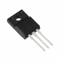
Package Dimensions
unit : mm (typ) 7509-002
10.0 3.2 4.5 2.8
3.5
7.2 16.0
16.1
0.9 1.2 0.75
3.6
1.2
14.0
0.7
123
2.4
1 : Gate 2 : Drain 3 : Source SANYO : TO-220FI(LS)
2.55
2.55
Switching Time Test Circuit
VIN 10V 0V VIN ID=8A RL=25Ω VDD=200V
0.6
Avalanche Resistance Test Circuit
L ≥50Ω RG
D
PW=10µs D.C.≤0.5%
VOUT
2SK4085LS 10V 0V 50Ω VDD
G
2SK4085LS P.G RGS=50Ω
S
No. A0553-2/5
�2SK4085LS
45
ID -- VDS
Tc=25°C
15V
10V
45
ID -- VGS
VDS=20V Tc= --25°C 25°C
40 35
40 35
Drain Current, ID -- A
30 25 20 15 10 5 0 0 5 10 15 20 25
8V
Drain Current, ID -- A
30 25 20 15 10 5 0
75°C
6V VGS=5V
30 IT11732
0
2
4
6
8
10
12
14
16
18
20
Drain-to-Source Voltage, VDS -- V
1.2
RDS(on) -- VGS
Gate-to-Source Voltage, VGS -- V
1.0
IT11733
RDS(on) -- Tc
ID=8A
0.9
Static Drain-to-Source On-State Resistance, RDS(on) -- Ω
1.0
Static Drain-to-Source On-State Resistance, RDS(on) -- Ω
0.8 0.7 0.6 0.5 0.4 0.3 0.2 0.1 0 --50 --25 0 25 50 75 100 125 150
0.8
0.6
Tc=75°C
0.4
=8 ID
A,
V
=1 GS
0V
25°C --25°C
0.2
0 3 5 7 9 11 13 15 IT11734
Gate-to-Source Voltage, VGS -- V
3
Case Temperature, Tc -- °C
5 3 2 10 7 5 3 2 1.0 7 5 3 2
IT11735
⏐yfs⏐ -- ID
IS -- VSD
VGS=0V
Forward Transfer Admittance, ⏐yfs⏐ -- S
2
VDS=10V
7 5 3 2
2
5°C --2 c= °C T 75
Source Current, IS -- A
10
5°C
7 5 3 0.1
3 2 2 3 5 7 1.0 2 3 5 7 10 2 3 5 0.01 0.2
0.4
0.6
--25°C
0.8
1.0
0.1 7 5
Tc=7 5°C 25°C
1.0
1.2
1.4 IT11737
Drain Current, ID -- A
1000 7
IT11736 10000 7 5 3 2 1000 7 5 3 2 100 7 5 3 2
SW Time -- ID
Ciss, Coss, Crss -- VDS
f=1MHz
Diode Forward Voltage, VSD -- V
Switching Time, SW Time -- ns
5 3 2
VDD=200V VGS=10V
Ciss, Coss, Crss -- pF
Ciss
td (off)
100 7 5 3 2
Coss
tr
tf
td(on)
Crss
10 0.1
10 2 3 5 7 1.0 2 3 5 7 10 2 3 5 7 0 5 10 15 20 25 30 35 40 45 50
Drain Current, ID -- A
IT11738
Drain-to-Source Voltage, VDS -- V
IT11739
No. A0553-3/5
�2SK4085LS
10 9
VGS -- Qg
VDS=200V ID=16A
2 100 7 5 3 2
ASO
IDP=60A
IDc(*1)=16A IDpack(*2)=11A
DC
PW