LB1860, LB1860M,
LB1861, LB1861M
www.onsemi.com
Monolithic Digital IC
Two-Phase Half-Wave
Variable Speed
Fan Motor Driver
Overview
The LB1860 series ICs are drivers for two-phase unipolar drive DC
brushless fan motors. They have functions such as driving, lock
protection, restart and speed control.
Features
Two-speed mode select function requiring less external component
additions : Full speed and Low speed. Or, thermistor-controlled
continuous variable-speed function according to ambient operation
temperatures.
Motor starts rotating at a low speed.
PDIP10 / DIP10S (300 mil)
[LB1860, LB1861]
Motor lock protection and automatic return circuit built in
Output transistors: Output current IO = 1.5 A, output circuit protection
Zener diodes
(LB1860 : M-Vz = 57 V/ LB1861: M-Vz = 32 V)
Enables low-level noise protection with chip capacitor.
Built-in thermal shutdown circuit Built-in rotation detect function
(Drive mode: ‘‘L’’, Stop mode: ‘‘H’’)
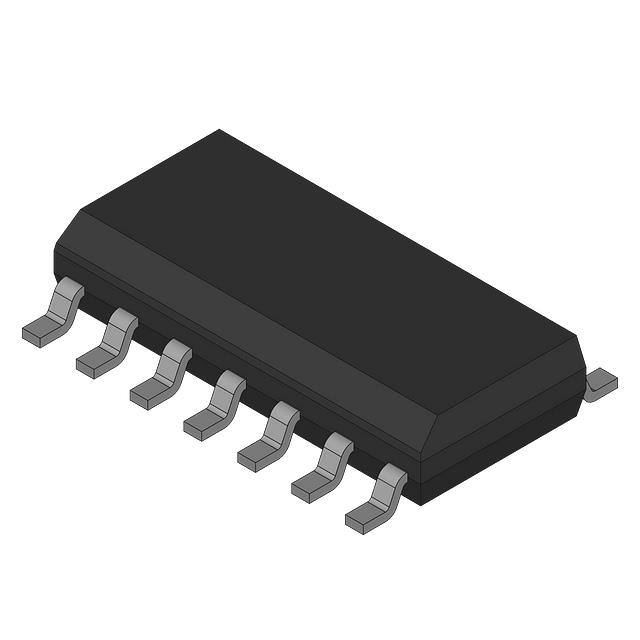
SOIC14 W / MFP14S (225 mil)
[LB1860M, LB1861M]
The LB1860 series can be operated from either 12 V or 24 V power
supply by changing an external resistor.
(Strong protection against power supply surge)
Connectable direct to a Hall element
ORDERING INFORMATION
See detailed ordering and shipping information on page 9 of this data sheet.
© Semiconductor Components Industries, LLC, 2017
August 2017 - Rev. 1
1
Publication Order Number :
LB1860_60M_61_61M/D
�LB1860, LB1860M, LB1861, LB1861M
Specifications
Absolute Maximum Ratings at Ta = 25 °C, ( ): LB1860M, LB1861M
Parameter
Symbol
Conditions
Ratings
t 20 ms
Unit
Maximum input current
ICC max
Output supply voltage
VOUT
Internal
Output current
IOUT
1.5
A
RD flow-in current
IRD
10
mA
RD supply voltage
VRD
50
V
200
Pd1 max
Allowable power dissipation
Mounted on 20 15 1.5 mm glass epoxy board
Pd2 max
mA
V
1.1
W
(0.8)
W
Operating temperature
Topr
–30 to +80
°C
Storage temperature
Tstg
–55 to +125
°C
Stresses exceeding those listed in the Maximum Ratings table may damage the device. If any of these limits are exceeded, device functionality should not be assumed,
damage may occur and reliability may be affected.
Allowable Operating Ranges at Ta = 25 °C
Parameter
Symbol
Input current range
Conditions
Ratings
ICC
Common-mode input voltage range
Unit
6.0 to 50
VICM
mA
0 to VIN –1.5
V
Functional operation above the stresses listed in the Recommended Operating Ranges is not implied. Extended exposure to stresses beyond the Recommended
Operating Ranges limits may affect device reliability.
Electrical Characteristics at Ta = 25 °C, ICC = 10 mA
Parameter
Output limiting voltage
Output saturation voltage
Input voltage
Amp input offset voltage
Amp input bias current
RD output saturation
voltage
C flow-out current
C discharge current
Comparator input threshold
voltage
Ct discharge voltage
Rt input current
Rt comparator voltage
Thermal protection circuit
operating voltage
Thermal protection circuit
hysteresis
Symbol
VOLM1
VO sat1
VO sat2
VO sat3
VIN
VOFF
IBA
VRD (sat)
Conditions
LB1860, 1860M: IO = 0.1 A
LB1861, 1861M: IO = 0.1 A
IO = 0.5 A
IO = 1.0 A
IO = 1.5 A
ICC = 7.0 mA
min
54
30
6.4
–7.0
–250
IRD = 5 mA
typ
57
32
0.95
1.15
1.4
6.7
0
max
60
34
1.2
1.5
2.0
7.0
7.0
Unit
V
V
V
V
V
V
mV
nA
0.15
0.3
V
3.9
0.50
0.8 VIN
0.47 VIN
0.2 VIN
–350
0.62 VIN
5.0
0.65
0.83
0.50
0.22
–240
0.65
μA
μA
V
V
V
μA
V
IC1
IC2
VTH1
VTH2
Vct
IRT
VRT
C = GND
C = VIN
TSD
Design target
180
°C
TSD
Design target
40
°C
2.7
0.35
0.77
0.44
0.18
–440
0.59
VRT = GND
RT = OPEN
Product parametric performance is indicated in the Electrical Characteristics for the listed test conditions, unless otherwise noted. Product performance may not be
indicated by the Electrical Characteristics if operated under different conditions.
www.onsemi.com
2
�LB1860, LB1860M, LB1861, LB1861M
Pin Assignments
Top view
Top view
Block Diagram and Application Circuit
Constant
current
circuit
0.47 to 10 μ
Output timing control
Unit (resistance: , capacitance: F)
( ): MFP14S
Figure 1
Truth Table
( ): LB1860M, 1861M
IN+
IN–
Ct
Rt1
Rt2
CR
OUT1
H
L
H
L
—
L
L
H
H
L
—
L
(H)
(L)
—
—
(H)
(L)
(H)
—
—
(H)
—
—
L
H
—
—
—
—
OUT2
RD
Mode
H
L
L
Full speed
L
H
L
Full speed
(L)
(H)
(L)
(L)
(Full speed)
(L)
(L)
(H)
(L)
(Full speed)
L
L
H
H
L
Low speed
—
H
H
H
H
Lock protection
www.onsemi.com
3
�LB1860, LB1860M, LB1861, LB1861M
Designer’s Notes
.
(1) Variable-speed circuit (Rt and Ct pins) — Refer to the application circuit diagram
The time constant gained by external components C2 and R2 is used to set the length of an ‘off’ operation time period after
phase switching. This means that the variable-speed operations can be performed by changing the ‘on’ operation time of each
phase through the duty control.
The sawtooth waveform signals are generated by the C2-R2 time constant. The voltage of this signal (Ct pin voltage) increases
from 1.3 V to 4.0 V (Vct) at each phase switching. That is, during this period, the driver becomes inactive (toff), in which
output circuit is turned off.
If VCC 4.0 V, the driver IC remains active (ton) until the next phase switching. During this period, output circuit is turned on.
If the active drive time of each phase is assumed to ‘to’, the following relation can be established:
.
.
.
to
=
toff
+
ton
Fixed
constant
Rotation speed
proportional constant
toff = 0.69 C2R2 ........................................1
. From this relation, it can be observed that the ‘t ’ and ‘t
.
o
on’ are in proportional relation with each other, and that the ‘ton/to’
equals the ‘on’ time duty. As a result, a certain rotation speed can be fixed despite the fact that rotation speed exclusively
depends on each motor.
At the start, the ‘ton’ value becomes longer while the ‘toff’ value remains unchanged. This means that the ‘toff/to’ duty becomes
small enough compared to normal rotation mode. Therefore, the same start torque as that of the full speed rotation can be
obtained because the ‘on’ operation time duty increases. This enables the motor to start at a very low speed.
voltage (V pin)
.(2)TheSupply
LB1860 has the internal parallel regulator which supplies power to the Hall amplifier circuit and the control block.
IN
.
.
.
Therefore, the driver ICs are not affected by power source fluctuations and kickbacks from the motor. They maintain the stable
operations even if noise signals such as surge are generated.
Set the resistance R1 between VCC and VIN so that the ICC current of 6 mA to 50 mA can flow onto the VIN pin within the
supply voltage range of a fan motor.
VIN is 6.7 V typ at ICC = 7 mA.
The current flowing into VIN is calculated using the equation shown below.
ICC
. Consideration given to surge voltage
. The maximum allowable current at V
IN
Vsurge
=
=
VCC – VIN
R1
............................ 2
pin is 200 mA. Therefore, the pin is designed to withstand abnormal positive voltage of:
VIN + R1 200 mA ............................................ 3
input pin voltage (Pins IN , IN )
.(3)SetHall
the voltage levels of the input pin for the Hall element output and the Hall element output voltage to within the range of
– 1.5 V.
. 0TheV togainV between
the hall input pin and the output pin is 100 dB or greater. The offset voltage of the hall input amp is 7 mV,
–
+
IN
therefore, the hall element output must be set with the offset voltage (7 mV) considered.
.
.
.
.
(4) Output transistor (Pins OUT1, OUT2)
Output current
IO = 1.5 A max
Output saturation voltage
VO sat = 1.15 V/1.0 A typ
Output limiting voltage
VOLM = 57 V typ (LB1860, 1860M)
VOLM = 32 V typ (LB1861,1861M)
Since the LB1860 series have a protect zener diode between collector and base, the kickback voltage induced by the coil is cut
at VOLM = 57 V (32 V). When external capacitors are connected between OUT and GND, the capacitance should not exceed
10 μF.
www.onsemi.com
4
�LB1860, LB1860M, LB1861, LB1861M
.
.
(5) Output protection function (C pin)
Capacitor pin used in forming an automatic return circuit.
If rotation is stopped due to overload, the pin voltage level increases and then forces the output to become inactive. In this case,
after proper load adjustment, the output returns to the ‘drive’ mode from the ‘stop’ mode automatically. By changing the
capacitor value, the lock detect time period can be set.
For C marked with 1 μF
Rotation
Output ON
Lock detect time
Lock protect time (output ON)
(output OFF)
Output OFF
Output
ON
Approximately 2 sec.
Approximately 1 sec.
Approximately 6 sec.
Output OFF
Lock
Rotation
Lock release
Automatic Return Circuit C Pin Voltage
1
2
3
4
When a fan is rotating, the capacitor is charged at 4 μA (typ) and discharged through the C with pulses according to the
rotational speed.
When a fan is locked, no discharge occurs through the C and the C voltage rises, turning OFF the output at 0.8 VIN.
When the output is turned OFF, discharge occurs through the C at 0.5 μA (typ). If the lock is not released when the C voltage
drops to VTH2, the capacitor is charged to VTH1 again. (At this moment, the output is turned ON.) These operations 2 and
3 repeated at a cycle of approximately ton : toff = 1:6 protect a motor.
If the lock is released when the C voltage drops to VTH2, the output is turned ON, starting rotation.
Rotation detect signal (RD pin)
.(6)Open
collector output (Drive mode: ‘‘L’’, Stop mode: ‘‘H’’)
noise reducing (Pins B1, B2)
.(7)BaseRadio
pin of Darlington connection output transistor
. If radio noises need to be processed properly, the following actions should be taken:
1 Connect a capacitor of 0.01 μ to 0.1 μF between B1 and B2.
2 Connect a capacitor of 0.001 μ to 0.01 μF between OUT and B.
If output causes oscillation, add a resistor of 200 to 1 k in series with a capacitor.
Thermal shutdown function
.(8)Shutdown
the driver output in case of coil short-circuiting and abnormal IC heating.
www.onsemi.com
5
�LB1860, LB1860M, LB1861, LB1861M
Thermistor-controlled Application Circuit Example
Noise elimination
capacitor
Use of a thermistor enables motor speed to
be sensitive to the operating ambient
temperature.
The Rt pin voltage at Ta = 20 °C has
1.42 ms of ‘toff’ as calculated in expression
4 with the application constant of Figure 2.
However, the Rt pin voltage at Ta = 40 °C
is reduced into less than the Vct (= 1.3 V)
level, which results in a 0 of ‘toff’. This
means the 100% duty.
t = –C2 R21n
Figure 2
(VIN – VRt)
............. 4
VIN – VCt
( ): MFP14S
Unit (resistance: , capacitance: F)
Output Timing Chart
Hall input
Discharge pulse
Ct voltage
Output ‘off’ signal
OUT1 current
All-phase ON waveform
Control output waveform
OUT2 current
Figure 3
www.onsemi.com
6
�LB1860, LB1860M, LB1861, LB1861M
Package Dimensions
unit : mm
[LB1860, LB1861]
to
PDIP10 / DIP10S (300 mil)
CASE 646AK
ISSUE O
www.onsemi.com
7
�LB1860, LB1860M, LB1861, LB1861M
Package Dimensions
unit : mm
[LB1860M, LB1861M]
SOIC14 W / MFP14S (225 mil)
CASE 751CB
ISSUE A
to
(Unit: mm)
1.10
SOLDERING FOOTPRINT*
GENERIC
MARKING DIAGRAM*
5.70
XXXXXXXXXX
YMDDD
1.00
0.47
NOTE: The measurements are not to guarantee but for reference only.
*For additional information on our Pb-Free strategy and soldering
details, please download the ON Semiconductor Soldering and
Mounting Techniques Reference Manual, SOLDERRM/D.
www.onsemi.com
8
XXXXX = Specific Device Code
Y = Year
M = Month
DDD = Additional Traceability Data
*This information is generic. Please refer to
device data sheet for actual part marking.
�LB1860, LB1860M, LB1861, LB1861M
ORDERING INFORMATION
Device
Package
Shipping (Qty / Packing)
LB1860M-TLM-E
SOIC14 W / MFP14S (225 mil)
(Pb-Free / Halogen Free)
1000 / Tape & Reel
LB1860M-TLM-H
SOIC14 W / MFP14S (225 mil)
(Pb-Free / Halogen Free)
1000 / Tape & Reel
LB1860M-W-AH
SOIC14 W / MFP14S (225 mil)
(Pb-Free / Halogen Free)
1000 / Tape & Reel
LB1861M-TLM-E
SOIC14 W / MFP14S (225 mil)
(Pb-Free / Halogen Free)
1000 / Tape & Reel
LB1861M-TLM-H
SOIC14 W / MFP14S (225 mil)
(Pb-Free / Halogen Free)
1000 / Tape & Reel
LB1861M-W-AH
SOIC14 W / MFP14S (225 mil)
(Pb-Free / Halogen Free)
1000 / Tape & Reel
† For information on tape and reel specifications, including part orientation and tape sizes, please refer to our Tape and Reel
Packaging Specifications Brochure, BRD8011/D. http://www.onsemi.com/pub_link/Collateral/BRD8011-D.PDF
ON Semiconductor and the ON Semiconductor logo are trademarks of Semiconductor Components Industries, LLC dba ON Semiconductor or its subsidiaries
in the United States and/or other countries. ON Semiconductor owns the rights to a number of patents, trademarks, copyrights, trade secrets, and other
intellectual property. A listing of ON Semiconductor’s product/patent coverage may be accessed at www.onsemi.com/site/pdf/Patent-Marking.pdf. ON
Semiconductor reserves the right to make changes without further notice to any products herein. ON Semiconductor makes no warranty, representation or
guarantee regarding the suitability of its products for any particular purpose, nor does ON Semiconductor assume any liability arising out of the application or
use of any product or circuit, and specifically disclaims any and all liability, including without limitation special, consequential or incidental damages. Buyer is
responsible for its products and applications using ON Semiconductor products, including compliance with all laws, regulations and safety requirements or
standards, regardless of any support or applications information provided by ON Semiconductor. “Typical” parameters which may be provided in ON
Semiconductor data sheets and/or specifications can and do vary in different applications and actual performance may vary over time. All operating parameters,
including “Typicals” must be validated for each customer application by customer’s technical experts. ON Semiconductor does not convey any license under its
patent rights nor the rights of others. ON Semiconductor products are not designed, intended, or authorized for use as a critical component in life support
systems or any FDA Class 3 medical devices or medical devices with a same or similar classification in a foreign jurisdiction or any devices intended for
implantation in the human body. Should Buyer purchase or use ON Semiconductor products for any such unintended or unauthorized application, Buyer shall
indemnify and hold ON Semiconductor and its officers, employees, subsidiaries, affiliates, and distributors harmless against all claims, costs, damages, and
expenses, and reasonable attorney fees arising out of, directly or indirectly, any claim of personal injury or death associated with such unintended or
unauthorized use, even if such claim alleges that ON Semiconductor was negligent regarding the design or manufacture of the part. ON Semiconductor is an
Equal Opportunity/Affirmative Action Employer. This literature is subject to all applicable copyright laws and is not for resale in any manner.
www.onsemi.com
9
�