Ordering number : ENA1172A
LV8761V
Bi-CMOS LSI
Forward/Reverse H-bridge Driver
http://onsemi.com
Overview
The LV8761V is an H-bridge driver that can control four operation modes (forward, reverse, brake, and standby) of a
motor. The low on-resistance, zero standby current, highly efficnet IC is optimal for use in driving brushed DC motors
for office equipment.
Features
• Forward/reverse H-bridge motor driver: 1 channel
• Built-in current limiter circuit
• Built-in thermal protection circuit
• Built-in short-circuit protection function
• Unusual condition warning output pin
• Short-circuit protection circuit selectable from latch-type or auto reset-type
Specifications
Absolute Maximum Ratings at Ta = 25°C
Parameter
Supply voltage
Symbol
Unit
V
VCC max
6
V
IO peak
Output continuous current
IO max
Allowable power dissipation
Ratings
38
Output peak current
Logic input voltage
Conditions
VM max
tw ≤ 20ms, duty 5%
VIN
Pd max
Mounted on a specified board. *
4
A
3
A
-0.3 to VCC+0.3
V
3.15
W
Operating temperature
Topr
-20 to +85
°C
Storage temperature
Tstg
-55 to +150
°C
* Specified circuit board : 90mm×90mm×1.6mm, glass epoxy 2-layer board (2S0P), with backside mounting.
Stresses exceeding Maximum Ratings may damage the device. Maximum Ratings are stress ratings only. Functional operation above the Recommended Operating
Conditions is not implied. Extended exposure to stresses above the Recommended Operating Conditions may affect device reliability.
Semiconductor Components Industries, LLC, 2013
May, 2013
30310 SY 20100223-S00008 / 42308 MS PC 20080331-S00003 No.A1172-1/13
�LV8761V
Allowable Operating Ratings at Ta = 25°C
Parameter
Supply voltage range
Symbol
Conditions
Ratings
Unit
VM
9 to 35
VCC
3 to 5.5
V
V
VREF input voltage
VREF
0 to VCC-1.8
V
Logic input voltage
VIN
0 to VCC
V
Electrical Characteristics at Ta = 25°C, VM = 24V, VCC = 5V, VREF = 1.5V
Parameter
Symbol
Ratings
Conditions
min
typ
Unit
max
General
Standby mode current drain 1
IMst
PS = “L”
1
μA
Standby mode current drain 2
ICCst
PS = “L”
1
μA
Operating mode current drain 1
IM
PS = “H”, IN1 = “H”, with no load
1
1.3
mA
Operating mode current drain 2
ICC
PS = “H”, IN1 = “H”, with no load
3
4
mA
5
5.25
VREG output voltage
VREG
IO = -1mA
4.75
V
VCC low-voltage cutoff voltage
VthVCC
2.5
2.7
2.9
V
Low-voltage hysteresis voltage
VthHIS
120
150
180
mV
Thermal shutdown temperature
TSD
Design guarantee *
155
170
185
°C
ΔTSD
Design guarantee *
Ron1
IO = 3A, sink side
Ron2
IO = -3A, source side
Thermal hysteresis width
°C
40
Output block
Output on resistance
0.2
0.25
Ω
0.32
0.40
Ω
50
μA
Rising time
tr
10% to 90%
200
500
ns
Falling time
tf
90% to 10%
200
500
ns
Output leakage current
Input output delay time
IOleak
VO = 35V
tpLH
IN1 or IN2 to OUTA or OUTB (L → H)
550
700
ns
tpHL
IN1 or IN2 to OUTA or OUTB (H → L)
550
700
ns
28.7
29.8
V
250
500
μs
140
165
kHz
Charge pump block
Step-up voltage
VGH
VM = 24V
Rising time
tONG
VG = 0.1μF
Oscillation frequency
Fcp
28.0
115
Control system input block
Logic pin input current 1
IINL
VIN = 0.8V adaptive pin : PS
5.6
8
10.4
μA
IINH
VIN = 5V adaptive pin : PS
56
80
104
μA
IINL
VIN = 0.8V adaptive pin : IN1, IN2, EMM
5.6
8
10.4
μA
IINH
VIN = 5V adaptive pin : IN1, IN2, EMM
35
50
65
μA
Logic pin input H-level voltage
VINH
adaptive pin : PS, IN1, IN2, EMM
2.0
Logic pin input L-level voltage
VINL
adaptive pin : PS, IN1, IN2, EMM
Logic pin input current 2
V
0.8
V
Current limiter block
VREF input current
IREF
Current limit comparator
Vthlim
μA
-0.5
VREF = 1.5V
0.285
0.3
0.315
V
3.5
5
6.5
μA
1
1.2
V
0.3
0.4
V
threshold voltage
Short-circuit protection block
SCP pin charge current
Iscp
Comparator threshold voltage
Vthscp
EMO output saturation voltage
Vemo
SCP = 0V
0.8
IO = 500μA
* Design guarantee value and no measurement is made.
No.A1172-2/13
�LV8761V
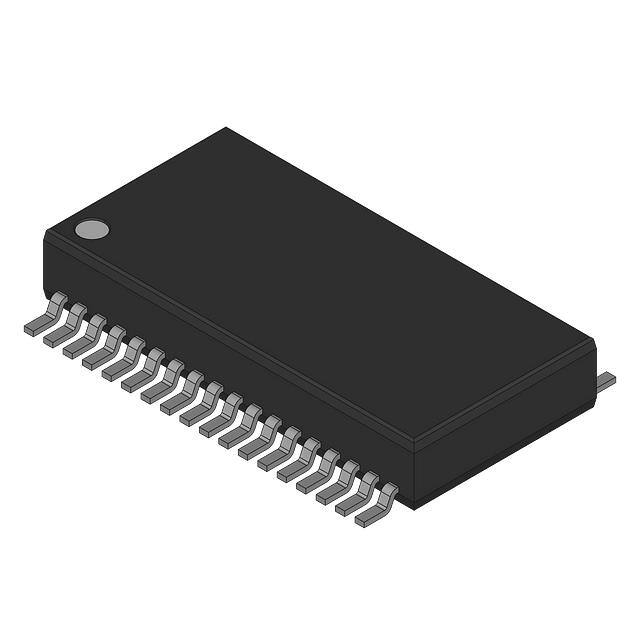
Package Dimensions
unit : mm (typ)
3361
SIDE VIEW
TOP VIEW
BOTTOM VIEW
15.0
36
(3.5)
0.5
5.6
7.6
(4.0)
1 2
0.3
0.8
0.2
0.1
(1.5)
SIDE VIEW
1.7 MAX
(0.7)
SANYO : SSOP36J(275mil)
Pin Assignment
VCC 1
36 EMM
PGND 2
35 SCP
34 VREF
NC 4
33 NC
NC 5
32 NC
OUTB 6
31 NC
OUTB 7
30 IN2
RNF 8
29 IN1
RNF 9
VM 10
LV8761V
NC 3
28 NC
27 REG5
VM 11
26 CP1
OUTA 12
25 CP2
OUTA 13
24 NC
NC 14
23 GND
NC 15
22 NC
NC 16
21 VG
PS 17
20 NC
GND 18
19 EMOT
Top view
No.A1172-3/13
�LV8761V
Pd max – Ta
Allowable power dissipation, Pd max – W
3.5
*1
3.15
*2
2.05
3.0
2.5
2.0
1.64
1.5
1.07
1.0
0.5
*1 With Exposed Die-Pad substrate
*2 Without Exposed Die-Pad
0
– 20
0
20
40
60
80
100
Ambient temperature, Ta – °C
Substrate Specifications (Substrate recommended for operation of LV8761T)
Size
: 90mm × 90mm × 1.6mm (two-layer substrate [2S0P])
Material
: Glass epoxy
Copper wiring density : L1 = 95% / L2 = 95%
L1 : Copper wiring pattern diagram
L2 : Copper wiring pattern diagram
Cautions
1) The data for the case with the Exposed Die-Pad substrate mounted shows the values when 90% or more of the
Exposed Die-Pad is wet.
2) For the set design, employ the derating design with sufficient margin.
Stresses to be derated include the voltage, current, junction temperature, power loss, and mechanical stresses such as
vibration, impact, and tension.
Accordingly, the design must ensure these stresses to be as low or small as possible.
The guideline for ordinary derating is shown below :
(1)Maximum value 80% or less for the voltage rating
(2)Maximum value 80% or less for the current rating
(3)Maximum value 80% or less for the temperature rating
3) After the set design, be sure to verify the design with the actual product.
Confirm the solder joint state and verify also the reliability of solder joint for the Exposed Die-Pad, etc.
Any void or deterioration, if observed in the solder joint of these parts, causes deteriorated thermal conduction,
possibly resulting in thermal destruction of IC.
No.A1172-4/13
�GND
VCC
EMOT
PS
VREG
VG
EMM
SCP
Short-circuit
Protection Circuit
Oscillation
circuit
LVS
TSD
Reference
Voltage
Circuit
Charge pump
CP1 CP2
VM
OUTA
OUTB
IN1
IN2
Output control
logic
M
Current
Limiter
Circuit
RNF
+
+
VREF
PGND
LV8761V
Block Diagram
Output preamplifier stage
Output preamplifier stage
+ -
+ -
No.A1172-5/13
�LV8761V
Pin Functions
Pin No.
Pin Name
Pin Functtion
29
IN1
Output control signal input pin 1.
30
IN2
Output control signal input pin 2.
36
EMM
Short-circuit protection circuit mode
Equivalent Circuit
VCC
switching pin.
10kΩ
100kΩ
GND
17
PS
Power save signal input pin.
VCC
50kΩ
10kΩ
10kΩ
50kΩ
GND
34
VREF
Reference voltage input pin for output
VCC
current limit setting.
500Ω
GND
35
SCP
Short-circiut protection circuit, detection
time setting capacitor connection pin.
VCC
500Ω
GND
1
VCC
Power supply connection pin for control
block.
Continued on next page.
No.A1172-6/13
�LV8761V
Continued from preceding page.
Pin No.
Pin Name
10, 11
VM
Motor power-supply connection pin.
Pin Functtion
12, 13
OUTA
OUTA output pin.
8, 9
RNF
Current sense resistor connection pin.
6, 7
OUTB
OUTB output pin.
2
PGND
Power ground.
Equivalent Circuit
10 11
REG5
6
7
12
13
500Ω
500Ω
8 9
2
GND
26
CP1
Charge pump capacitor connection pin.
25
CP2
Charge pump capacitor connection pin.
21
VG
Charge pump capacitor connection pin.
26
10 11
25
21
100Ω
REG5
GND
27
REG5
Internal reference voltage output pin.
VM
74kΩ
2kΩ
25kΩ
GND
19
EMOT
Unusual condition warning output pin.
VCC
500Ω
GND
18, 23
GND
Ground.
No.A1172-7/13
�LV8761V
DC Motor Driver
1.DCM output control logic
Contol Input
PS
IN1
Output
IN2
OUTA
OUTB
Mode
L
*
*
OFF
OFF
Standby
H
L
L
OFF
OFF
Output OFF
H
H
L
H
L
CW (forward)
H
L
H
L
H
CCW (reverse)
H
H
H
L
L
Brake
2.Current limit control timing chart
Limit current
Output current
OUTA
OUTB
toff
CHARGE
SLOW
Braking operation time in current limit mode can be set by connecting a capacitor between SCP and GND pins. This
setting is the same as the time setting required to turn off the outputs when an output short-circuit occurs as explained in
the section entitled "Output Short-circuit Protection Function." See "Output Short-circuit Protection Function," for the
settinig procedure.
3.Setting the current limit value
The current limit value of the DCM driver is determined by the VREF voltage and the resistance (RNF) connected
across the RNF and GND pins using the following formula :
Ilimit [A] = (VREF [V] /5) /RNF [Ω])
Assuming VREF = 1.5V, RNF = 0.2Ω, the current limit is :
Ilimit = 1.5V/5/0.2Ω = 1.5A
No.A1172-8/13
�LV8761V
Output short-circuit protection function
The LV8761V incorporates an output short-circuit protection circuit that turns off the output to prevent the IC from
fatal damage when the output is short-circuited due to short-to-power or short-to-ground fault. Either the “latch-type,”
in which the output off state is latched when the short-circuit protection circuit is activated, or “auto reset-type,” in
which the output on/off states are repeated when the short-circuit protection circuit is activated, can be selected.
EMM Pin
Short-circuit Protection Mode
L
Latch type
H
Auto reset type
1.Protection function operation (Latch method)
The short-circuit protection circuit is activated when it detects the output short-circuit state. If the short-circuit state
continues for the internally preset period (≈ 4μs), the protection circuit turns off the output from which the short-circuit
state has been detected. Then it turns the output on again after a lapse of the timer latch time described later. If the
short-circuit state is still detected, it changes all the outputs to the standby mode and retains the state. The latched state
is released by setting the PS to L.
Output ON
H-bridge
output state
Output ON
Output OFF
Standby state
Threshold voltage
4μs
SCP voltage
Short-circuit
detection state
Short- Release
circuit
Short-circuit
Internal counter
1st counter
start
1st counter 1st counter
stop
start
1st counter
end
2nd counter
start
2nd counter
end
2.How to set the SCP pin constant (timer latch-up setting)
The user can set the time at which the outputs are turned off when a short-circuit occurs by connecting a capacitor
across the SCP and GND pins. The value of the capacitor can be determined by the following formula :
Timer latch-up : Tocp
Tocp ≈ C × V/I [s]
V : Comparator threshold voltage (1V typical)
I : SCP charge current (5μA typical)
When a capacitor with a capacitance of 50pF is connected across the SCP and GND pins, for example, Tscp is
calculated as follows :
Tscp = 50pF × 1V/5μA = 10μs
No.A1172-9/13
�LV8761V
3.Auto Reset Type
The sequences up to the detection of an output short-circuit state are identical to those which are explained in Section 1,
"Protection Function Operation (Latch Type).
After output is turned off on detection of an output short-circuit condition, the internal counter starts counting and
repeats turning on and off the output as shown in the figure below.
This state continues until the overcurrent state is eliminated.
Exceeding the
over-current
detection
current
ON
OFF
Detection current
sequences
2ms (TYP)
ON
OFF
ON
Output current
SCP voltage
4.Unusual Condition Warning Output Pin (EMOT)
The LV8761V is provided with the EMOT pin which notifies the CPU of an unusual condition if the protection circuit
operates by detecting an abnormal condition of the IC. This pin is of the open-drain output type and requires a pull-up
resistor when to be used.
The EMOT pin is placed in the ON state when one of the following conditions occurs.
1. Shorting-to-power or shorting-to-ground occurs at the output pin and the output short-circuit protection circuit is
activated.
2. The IC junction temperature rises and the thermal protection circuit is activated.
The EMOT pin is set to the OFF state when the relevant protection operation is eliminated.
No.A1172-10/13
�LV8761V
Application Circuit Example
(When you use the current limit function)
- +
1 VCC
EMM 36
2 PGND
SCP 35
Control input
100pF
3 NC
VREF 34
4 NC
NC 33
5 NC
NC 32
6 OUTB
NC 31
7 OUTB
IN2 30
8 RNF
IN1 29
Control input
M
10 VM
- +
Control input
LV8761V
9 RNF
NC 28
REG5 27
11 VM
CP1 26
12 OUTA
CP2 25
13 OUTA
NC 24
14 NC
GND 23
15 NC
NC 22
16 NC
VG 21
17 PS
NC 20
18 GND
EMOT 19
Monitor
Setting the current limit value
When VCC = 5V,
Vref = 1.5V
Ilimit = Vref/5/RNF
= 1.5V/5/0.22Ω = 1.36A
Setting the current limit regeneration time and short-circuit detection time
Tscp ≈ C × V/I
= 100pF × 1V/5μA
= 20μs
No.A1172-11/13
�LV8761V
(When you do not use the current limit function)
- +
1 VCC
EMM 36
2 PGND
SCP 35
Control input
100pF
3 NC
VREF 34
4 NC
NC 33
5 NC
NC 32
6 OUTB
NC 31
7 OUTB
IN2 30
8 RNF
IN1 29
Control input
M
10 VM
- +
Control input
LV8761V
9 RNF
NC 28
REG5 27
11 VM
CP1 26
12 OUTA
CP2 25
13 OUTA
NC 24
14 NC
GND 23
15 NC
NC 22
16 NC
VG 21
17 PS
NC 20
18 GND
EMOT 19
Monitor
Setting at short-circuit state detection time
TSCP ≈ C·V/I
=100pF·1V/5µA
=20µs
*Do the following processing when you do not use the current limit function.
· It is short between RNF-GND.
· The terminal VREF is hung on suitable potential of VCC or less.
No.A1172-12/13
�LV8761V
ON Semiconductor and the ON logo are registered trademarks of Semiconductor Components Industries, LLC (SCILLC). SCILLC owns the rights to a number
of patents, trademarks, copyrights, trade secrets, and other intellectual property. A listing of SCILLC’s product/patent coverage may be accessed at
www.onsemi.com/site/pdf/Patent-Marking.pdf. SCILLC reserves the right to make changes without further notice to any products herein. SCILLC makes no
warranty, representation or guarantee regarding the suitability of its products for any particular purpose, nor does SCILLC assume any liability arising out of the
application or use of any product or circuit, and specifically disclaims any and all liability, including without limitation special, consequential or incidental
damages. “Typical” parameters which may be provided in SCILLC data sheets and/or specifications can and do vary in different applications and actual
performance may vary over time. All operating parameters, including “Typicals” must be validated for each customer application by customer’s technical
experts. SCILLC does not convey any license under its patent rights nor the rights of others. SCILLC products are not designed, intended, or authorized for use
as components in systems intended for surgical implant into the body, or other applications intended to support or sustain life, or for any other application in
which the failure of the SCILLC product could create a situation where personal injury or death may occur. Should Buyer purchase or use SCILLC products for
any such unintended or unauthorized application, Buyer shall indemnify and hold SCILLC and its officers, employees, subsidiaries, affiliates, and distributors
harmless against all claims, costs, damages, and expenses, and reasonable attorney fees arising out of, directly or indirectly, any claim of personal injury or
death associated with such unintended or unauthorized use, even if such claim alleges that SCILLC was negligent regarding the design or manufacture of the
part. SCILLC is an Equal Opportunity/Affirmative Action Employer. This literature is subject to all applicable copyright laws and is not for resale in any manner.
PS No.A1172-13/13
�