TN5D01A
Ordering number : ENA1446
SANYO Semiconductors
DATA SHEET
ExPD (Excellent-Performance Power & RF Device)
TN5D01A
Separately-Excited Step-Down
Switching Regulator
(Variable Output Type)
Features
•
•
•
•
•
•
High efficiency (ON resistance 100mΩ, Vertical-type P-ch Power MOSFET).
Over current protection function (Self recovery type).
Under voltage protection function.
Over temperature protection function (Self recovery type).
Soft start function (Variable subject to externally-connected capacitor).
Stand-by mode function (Compatible with soft start terminal).
Specifications
Absolute Maximum Ratings at Ta=25°C
Parameter
Maximum Input Voltage
Symbol
Maximum Output Current
VIN max
IO max
Drain-to-Source Voltage of built-in MOSFET
VDSS
Drain Current of built-in MOSFET (DC)
ID
IDP
Drain Current of built-in MOSFET (Pulse)
FB Pin Maximum Input Voltage
SS Pin Maximum Input Voltage
Conditions
PW≤10μs, duty cycle≤1%
Vfb
VSS
Allowable Power Dissipation
PD
Operating Temperature
Topr
Junction Temperature
Tj
Storage Temperature
Tstg
Tc=25°C
Ratings
Unit
57
V
5
A
--60
V
--9
A
--36
A
5
V
7
V
2.0
W
15
W
--25 to +125
°C
150
°C
--55 to +150
°C
Any and all SANYO Semiconductor Co.,Ltd. products described or contained herein are, with regard to
"standard application", intended for the use as general electronics equipment (home appliances, AV equipment,
communication device, office equipment, industrial equipment etc.). The products mentioned herein shall not
be intended for use for any "special application" (medical equipment whose purpose is to sustain life,
aerospace instrument, nuclear control device, burning appliances, transportation machine, traffic signal
system, safety equipment etc.) that shall require extremely high level of reliability and can directly threaten
human lives in case of failure or malfunction of the product or may cause harm to human bodies, nor shall they
grant any guarantee thereof. If you should intend to use our products for applications outside the standard
applications of our customer who is considering such use and/or outside the scope of our intended standard
applications, please consult with us prior to the intended use. If there is no consultation or inquiry before the
intended use, our customer shall be solely responsible for the use.
Specifications of any and all SANYO Semiconductor Co.,Ltd. products described or contained herein stipulate
the performance, characteristics, and functions of the described products in the independent state, and are
not guarantees of the performance, characteristics, and functions of the described products as mounted in the
customer' s products or equipment. To verify symptoms and states that cannot be evaluated in an
independent device, the customer should always evaluate and test devices mounted in the customer' s
products or equipment.
www.semiconductor-sanyo.com/network
71509IQ TK IM TC-00002025 No. A1446-1/11
�TN5D01A
Recommended Operating Conditions
Parameter
Input Voltage
Output Voltage
Output Current
Operating Temperature Range
Symbol
Conditions
VIN
VOUT
Ta=25°C
IOUT
Topr rec
Ta=25°C
Ratings
Unit
10 to 30
Ta=25°C, VOUT / VIN ≥ 0.1
V
2.7 to 4.9
V
0 to 5
A
--10 to + 85
°C
Electrical Characteristics at Ta=25°C, See Specified Test Circuit (VOUT=3.3V)
Parameter
Symbol
Conditions
Ratings
min
typ
Reference Voltage
VFB
η
VIN=20V, IOUT=3A
VIN=20V, IOUT=3A
1.12
Efficiency
V(BR)DSS
ID=--1mA, VIN, GND, Vfb, VSS=0V
--60
RDS(on)
ISW=5A
Drain-to-Source Breakdown Voltage
of built-in MOSFET
Drain-to-Source On Resistance
of built-in MOSFET
Switching Frequency
Freq
Maximum Duty
Duty max
VIN=20V, IOUT=3A
VIN=20V, Vfb=0V
Line Regulation
ΔVline
VIN=10 to 30V, IOUT=3A
Load Regulation
ΔVload
VIN=20V, IOUT=0.5 to 5A
Output Voltage Temperature Coefficient *1
ΔVO/ΔTa
VIN=20V, IOUT=3A, Ta=--25 to 125°C
Iocp
VIN=20V
Over-Current-Protection-Operation
-Threshold Current
Under-Voltage-Protection-Operation
-Threshold Voltage
Under-Voltage-Protection-Operation
-Release Voltage
Under-Voltage-Protection Hysteresis Voltage
Over-Temperature-Protection-Operation
-Threshold-Temperature *1
Over-Temperature-Protection-Operation
-Release Temperature *1
Over-Temperature-Protection-Operation
-Hysteresis Temperature *1
max
1.15
1.18
82
Unit
V
%
V
100
mΩ
120
150
180
88
92
96
%
30
60
mV
35
60
±0.33
kHz
mV
mV / °C
5.1
7.5
10
A
Vuvlo on
7.2
8.0
8.8
V
Vuvlo off
8.1
9.0
9.9
V
Vuvlo hys
1.0
V
Ttsd on
165
°C
Ttsd off
140
°C
Ttsd hys
25
°C
μA
SS Terminal Current
ISS
VIN=20V
10
Standby Operating Voltage
Vstb on
VIN=20V
0.3
Standby Current
Istb
VIN=20V, VSS=0V
V
500
μA
Note: the values with “*1” are our targeted values, but not guaranteed.
No. A1446-2/11
�TN5D01A
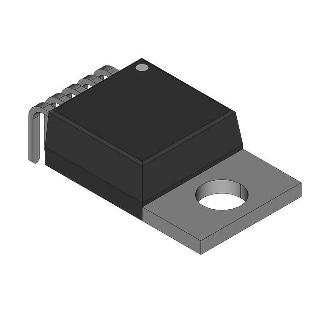
Package Dimensions
unit : mm (typ)
7531-001
10.0
4.5
3.2
21.4
17.5
(1.6)
16.0
7.2
3.5
2.8
8.9
2.4
0.9
0.5
12
3 45
0.7
1.27
3.81
2.54
1.27
2.75
2.54
1 : VIN
2 : GND
3 : SWOUT
4 : FB
5 : SS
SANYO : TO-220FI5H-HCC
Block Diagram
VIN 1
3 SWOUT
Under
Voltage
Protect
Over
Temperature
Protect
Over Current
Protect
SENSE
Pch MOSFET
OUTPUT
-COMP
+
OSC
SS 5
SOFTSTART
Band Gap
+
--
GND 2
AMP
4 FB
No. A1446-3/11
�TN5D01A
Pin Functions
Pin No.
Symbol
1
Function
Power Supply Input (Maximum 57V)
2
VIN
GND
3
SWOUT
Pulse Voltage Output
4
FB
Feedback from Output Voltage
5
SS
For Soft Start Capacitor Connection and Standby Mode Switching
GND
Application Circuit Example
SWOUT 3
1 VIN
VOUT
VIN
FB 4
5 SS
+
+
2 GND
GND
Forward Bias A S O
IDP= --36A
很抱歉,暂时无法提供与“TN5D01A-HCC11-E”相匹配的价格&库存,您可以联系我们找货
免费人工找货