ESD/EMI Protection for Color LCD Interfaces
PROTECTION PROTECTION PRODUCTS - EMIClampTM Description
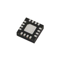
The EClampTM2342N is a low pass filter array with integrated TVS diodes. It is designed to suppress unwanted EMI/RFI signals and provide electrostatic discharge (ESD) protection in portable electronic equipment. This state-of-the-art device utilizes solidstate silicon-avalanche technology for superior clamping performance and DC electrical characteristics. They have been optimized for protection of color LCD panels in cellular phones and other portable electronics. The device consists of eight identical circuits comprised of TVS diodes for ESD protection, and a resistor capacitor network for EMI/RFI filtering. A series resistor value of 100Ω and a capacitance value of 20pF are used to achieve 30dB minimum attenuation from 1GHz to 2.5GHz. Each line features two stages of TVS diode protection. The TVS diodes provide effective suppression of ESD voltages in excess of 15kV (air discharge) and 8kV (contact discharge) per IEC 610004-2, level 4. The EClamp2342N is in a 16-pin, 0.5mm pitch QFN package. It measures 3.0 x 3.0 x 1.0mm. The small package makes it ideal for use in portable electronics such as cell phones, digital still cameras, and PDA’s.
EClamp2342N
PRELIMINARY
Features
Bidirectional EMI/RFI filter with integrated TVS for ESD protection
ESD protection to IEC 61000-4-2 (ESD) Level4, +/-15kV (air), +/-8kV (contact) Filter performance: 30dB minimum attenuation 1GHz to 2.5GHz T VS working voltage: 5V Resistor: 100Ω +/− 15% Input Capacitance: 20pF (VR = 0V) Protection and filtering for eight lines Solid-state technology
Mechanical Characteristics
16 pin QFN Nominal Dimensions: 3.0 x 3.0 x 1.0 mm Lead Pitch: 0.5mm Lead finish: Matte Tin Marking : Marking Code + Date Code Packaging : Tape and Reel per EIA 481
Applications
Color LCD Panel Protection Cell Phone CCD Camera Lines Clamshell Cell Phones Personal Digital Assistants (PDA’s)
Circuit Diagram
Package Configuration
16 1
LOW PASS FILTER
R = 100Ω, C=20pF (max) 16 Pin QFN (Top Side View) Maximum Dimensions (in mm)
1 www.semtech.com
Device Schematic (8X)
Revision 09/01/2004
�EClamp2342N
PROTECTION PRODUCTS Maximum Ratings
R ating ESD p er IEC 61000-4-2 (Air) ESD p er IEC 61000-4-2 (Contact) Junction Temp erature Op erating Temp erature Storage Temp erature Symbol VESD TJ Top TSTG Value +/- 17 +/- 12 125 -40 to +85 -55 to +150
PRELIMINARY
Units kV
o
C C C
o
o
Electrical Characteristics
P ar am et er T VS Reverse Stand-Off Voltage T VS Reverse Breakdown Voltage T VS Reverse Leakage Current Total Series Resistance Total Cap acitance
S y m b ol VRWM V BR IR R Cin
Con d i t i on s
Mi n i mu m
Ty p i c a l
M ax i m u m 5
Units V V µA Ohms pF
It = 1mA VRWM = 3.0V Each Line Inp ut to Gnd, Each Line VR = 0V, f = 1MHz Inp ut to Gnd, Each Line VR = 2.5V, f = 1MHz
6
8
10 0.5
85
100 16
115 20
Total Cap acitance
Cin
12
pF
2004 Semtech Corp.
2
www.semtech.com
�EClamp2342N
PROTECTION PRODUCTS Typical Characteristics
Typical Insertion Loss S21 (Each Line)
CH1 S21 LOG 6 dB / REF 0 dB 1: -8.4313 dB 280.123 MHz 0 dB -6 dB -12 dB -18 dB
2 1
PRELIMINARY
Analog Crosstalk (Each Line)
CH1 S 21 LOG 20 dB /REF 0 dB
2: -18.865 dB 900 MHz 3: -31.170 dB 1.8 GHz 4: -31.638 dB 2.5 GHz
-24 dB -30 dB
3 4
-36 dB -42 dB 1 MHz START. 030 MHz 10 MHz 100 MHz 3 1 GHz GHz . STOP 3000 000000 MHz
S TART. 030 M Hz . STOP 3000 000000 M Hz
ESD Clamping (+8kV Contact)
ESD Clamping (-8kV Contact)
Capacitance vs. Reverse Voltage (Normalized to 0 volts)
1.2
1.2
Series Resistance vs. Temperature (Normalized to 25 Degrees Celcius)
1
1.1
Capacitance - CJ (pF)
0.8
Series Resistance (Ohm) 1.0
0.6
0.4
0.9
0.2
f = 1 MHz
0.8
0 0 1 2 3 4 5
Reverse Voltage - VR (V)
0.7 -40
-30
-20
-10
0
10
20
30
40
50
60
70
80
Temperature (*C)
2004 Semtech Corp.
3
www.semtech.com
�EClamp2342N
PROTECTION PRODUCTS Applications Information
Device Connection The EClamp2342N is comprised of eight identical circuits each consisting of a low pass filter for EMI/RFI suppression and dual TVS diodes for ESD protection. The device is housed in a 16-pin Quad Flat No-Lead (QFN) package. Electrical connection is made via 16 pins located at the bottom of the device. A center tab serves as the ground connection. Pin connections are noted in the table to the right. The device is symmetrical and designed for easy PCB routing as shown in the layout example below. All path lengths should be kept as short as possible to minimize the effects of parasitic inductance in the board traces. Matte Tin Lead Finish Matte tin has become the industry standard lead-free replacement for SnPb lead finishes. A matte tin finish is composed of 100% tin solder with large grains. Since the solder volume on the leads is small compared to the solder paste volume that is placed on the land pattern of the PCB, the reflow profile will be determined by the requirements of the solder paste. Therefore, these devices are compatible with both lead-free and SnPb assembly techniques. In addition, unlike other lead-free compositions, matte tin does not have any added alloys that can cause degradation of the solder joint.
PRELIMINARY
Pin Identification and Configuration (Top Side View)
16 15 14 13 1 2 3 4 5678
Pin 3 - 10 1, 2, 11 - 16 Center Tab Identification Inp ut, Lines 1, 2, 3, 4, 5, 6, 7, 8 Outp ut Lines 1, 2, 3, 4, 5,6, 7, 8 Ground
12 11 10 9
Pin Configuration and Schematic
3
LOW PASS FILTER
2
7
LOW PASS FILTER
14
4
1
LOW PASS FILTER
8
LOW PASS FILTER
13
Layout Example (Top Side View)
Outputs 12 3456 78
5
16
LOW PASS FILTER
9
LOW PASS FILTER
12
6
LOW PASS FILTER
15
10
LOW PASS FILTER
11
I/O Lines 1 - 4
12 3456 Inputs 78
I/O Lines 5 - 8
2004 Semtech Corp.
4
www.semtech.com
�EClamp2342N
PROTECTION PRODUCTS Outline Drawing - 16L QFN
DIMENSIONS INCHES MILLIMETERS DIM MIN NOM MAX MIN NOM MAX
B
A A1 A2 b D D1 E E1 e L N aaa bbb .031 .040 .002 .000 (.008) .007 .010 .012 .114 .118 .122 .051 .057 .061 .114 .118 .122 .051 .057 .061 .020 BSC .012 .016 .020 16 .003 .004 0.80 1.00 0.00 0.05 (0.20) 0.18 0.25 0.30 2.90 3.00 3.10 1.30 1.45 1.55 2.90 3.00 3.10 1.30 1.45 1.55 0.50 BSC 0.30 0.40 0.50 16 0.08 0.10
PRELIMINARY
A
D
PIN 1 INDICATOR (LASER MARK)
E
A2 A aaa C A1 D1 e/2 LxN E/2 E1 2 1 N e
D/2
C
SEATING PLANE
bxN bbb
CAB
NOTES: 1. 2. CONTROLLING DIMENSIONS ARE IN MILLIMETERS (ANGLES IN DEGREES). COPLANARITY APPLIES TO THE EXPOSED PAD AS WELL AS THE TERMINALS.
Land Pattern - 16L QFN
H R
DIM
2x (C) 2x G 2x Z C G H R P X Y Z
DIMENSIONS INCHES MILLIMETERS
(.112) .079 .063 .006 .020 .012 .033 .146 (2.85) 2.00 1.60 0.15 0.50 0.30 0.85 3.70
4x Y X P
NOTES: 1.
THIS LAND PATTERN IS FOR REFERENCE PURPOSES ONLY. CONSULT YOUR MANUFACTURING GROUP TO ENSURE YOUR COMPANY'S MANUFACTURING GUIDELINES ARE MET.
2004 Semtech Corp.
5
www.semtech.com
�EClamp2342N
PROTECTION PRODUCTS Marking PRELIMINARY Ordering Information
Part Number Qty per Reel 3000 R eel Size 7 Inch
16 15 14 13 1 2 3 4
13 14 15 16 12 11 10 9 12 11 10 9 8765
Bottom View Showing Pin 1 Identifier
EClamp 2342N .TCT
2342N YYWW
5 678
1 2 3 4
EMIClamp and EClamp are marks of Semtech Corporation
Top View Showing Device Marking
Notes: 1) YYWW = Date Code (example: 0410 = 2004 year Week 10 2) Pin 1 indicated by bevel on the ground pad
Tape and Reel Specification
Tape Specifications
Device Orientation in Tape
Contact Information
Semtech Corporation Protection Products Division 200 Flynn Rd., Camarillo, CA 93012 Phone: (805)498-2111 FAX (805)498-3804
2004 Semtech Corp. 6 www.semtech.com
�
很抱歉,暂时无法提供与“ECLAMP2342N.TCT”相匹配的价格&库存,您可以联系我们找货
免费人工找货