Low Capacitance ESD/EMI Protection for SIM Card
PROTECTION PROTECTION PRODUCTS - EMIClampTM Description
The EClampTM2465T is a combination EMI filter and line termination device with integrated TVS diodes for use on SIM Card interfaces on cellular phones and other portable electronics. This state-of-the-art device utilizes solid-state silicon-avalanche technology for superior clamping performance and DC electrical characteristics. The device consists of three circuits that include series impedance matching resistors for proper termination of the SIM card interface. Termination resistor value of 100 Ohms is included on the Reset and Data lines and 47 Ohms on the CLK line. TVS diodes are also included on each line for ESD protection in excess of ±15kV (air discharge) and ±8kV (contact discharge) per IEC 610004-2, level 4. An additional TVS diode connection is included for protection of the voltage (Vcc) bus. The EClamp2465T is in a 8-pin, RoHS/WEEE compliant, SLP1713P8T package. It measures 1.7 x 1.3 mm with a nominal height of only 0.4mm. The leads are spaced at a pitch of 0.4mm and are finished with lead-free NiPdAu. The small package makes it ideal for use in portable electronics such as cell phones and digital still cameras.
EClamp2465T
PRELIMINARY
Features
Bidirectional EMI/RFI filter with integrated TVS for ESD protection
ESD protection to IEC 61000-4-2 (ESD) Level 4, ±15kV (air), ±8kV (contact) T VS working voltage: 5V Termination Resistors: 100 Ohms & 47 Ohms Capacitance: 10pF (Typical at VR = 0V) Protection and filtering for four lines Solid-state technology
Mechanical Characteristics
SLP1713P8T 8-pin package RoHS/WEEE Compliant Nominal Dimensions: 1.7 x 1.3 x 0.40 mm Lead Pitch: 0.4mm Lead finish: NiPdAu Marking: Marking Code + Date Code Packaging: Tape and Reel
Applications
SIM Card Cell Phone PDAs and Smartphones
Pin Configuration
Package Configuration
1.70
12
Data to Connector CLK to Connector
1
8
Data to IC CLK to IC Reset to IC
1.30
Gnd
Reset to Connector NC
4 5
0.40 BSC
Vcc to Connector
0.40
Pin Identification and Configuration (Top Side View)
Revision 09/24/2008 1
8 Pin SLP package (Bottom Side View) Nominal Dimensions in mm
www.semtech.com
�EClamp2465T
PROTECTION PRODUCTS Pin Identification and Configuration
Pin 1 2 3 4 5 6 7 8 Center tab Symbol Data CLK Reset NC Vcc Reset CLK Data GN D Identification Data Input (SIM Connector Side) Clock Input (SIM Connector Side) Reset Input (SIM Connector Side) N o Connect Power Supply ESD Protection (SIM Connector Side) Reset Output (IC Side) Clock input (IC Side) Data Output (IC Side) Ground connection
PRELIMINARY
8
7
6
5
Gnd 1 2 3 4
Pin Configuration (Top View)
Schematics & Component Values
Vcc (Pin 5)
100 Ω Data to Connector
(Pin 1)
Data to IC 47 Ω 100 Ω
(Pin 8)
CLK to Connector
(Pin 2)
CLK to IC
(Pin 7)
Reset to Connector
(Pin 3)
Reset to IC
(Pin 6)
GND TAB
© 2008 Semtech Corp.
2
www.semtech.com
�EClamp2465T
PROTECTION PRODUCTS Maximum Ratings
R ating ESD p er IEC 61000-4-2 (Air)1 ESD p er IEC 61000-4-2 (Contact) Junction Temp erature Op erating Temp erature Storage Temp erature Symbol VESD TJ Top TSTG Value +/- 18 +/- 10 125 -40 to +85 -55 to +150
PRELIMINARY
Units kV
o
C C C
o
o
Electrical Characteristics (T=25oC)
P ar am et er T VS Reverse Stand-Off Voltage T VS Reverse Breakdown Voltage T VS Reverse Leakage Current Reset Series Resistors Clk Series Resistors Data Series Resistors Total Cap acitance
S y m b ol VRWM V BR IR RRST R
CLK
Con d i t i on s
Mi n i mu m
Ty p i c a l
M ax i m u m 5
Units V V μA Ohms Ohms Ohms pF
It = 1mA VRWM = 5.0V Each Line Each Line Each Line Inp ut to Gnd, Each Line VR = 0V, f = 1MHz
6
8
10 0.5
85 40 85 8
100 47 100 10
115 55 115 12
RDATA Cin
Note: 1) ESD input at Pins 1, 2, 3, 5
© 2008 Semtech Corp.
3
www.semtech.com
�EClamp2465T
PROTECTION PRODUCTS Typical Characteristics
Typical Insertion Loss S21 (Pin 2 to 7)
CH1 S21 LOG 6 dB / REF 0 dB 1: -6.33460 dB 537.824 MHz 2: -8.4201 dB 800 MHz 3: -9.1592 dB 900 MHz
2 3
PRELIMINARY
Typical Insertion Loss S21 (Pin 1 to 8 and Pin 3 to 6)
CH1 S21 LOG 6 dB / REF 0 dB 1: -8.7516 dB 506.218 MHz 0 dB -6 dB -12 dB -18 dB
4 1 2 3
0 dB -6 dB
1
2: -11.352 dB 800 MHz 3: -12.208 dB 900 MHz 4: -17.795 dB 1.8 GHz
5
-12 dB -18 dB -24 dB -30 dB -36 dB -42 dB -48 dB
4
4
4: -14.622 dB 1.8 GHz 5: -18.026 dB 2.7 GHz
-24 dB -30 dB -36 dB -42 dB
5: -20.591 dB 2.5 GHz
1 MHz START.030 MHz
10 MHz
100 MHz
3 1 GHz GHz . STOP 3000 000000 MHz
-48 dB
1 MHz START. 030 MHz
10 MHz
100 MHz
3 1 GHz GHz . STOP 3000 000000 MHz
ESD Clamping (+8kV Contact)
ESD Clamping (-8kV Contact)
Note: Data is taken with a 10x attenuator
Note: Data is taken with a 10x attenuator
Normalized Capacitance vs. Reverse Voltage
1.1 1 0.9 0.8
C J(VR) / CJ(VR=0)
0.7 0.6 0.5 0.4 0.3 0.2 0.1 0 0 0.5 1 1.5 2 2.5 3 3.5 4 4.5 5
f = 1 MHz
Reverse Voltage - VR (V)
© 2008 Semtech Corp.
4
www.semtech.com
�EClamp2465T
PROTECTION PRODUCTS
Device Connection The EClamp2465T designed with ease of layout in mind. The package has flow through design which allows the designer to route the signals straight in and out between the SIM port connector and the SIM controller. The device is in a 8-pin SLP package. Electrical connection is made to the 8 pins located at the bottom of the device. A center tab serves as the ground connection. Pin connections are noted in Figure 1. Note that the ESD protection diodes are located at pins 1 - 3 for the data and clock lines. This means the device is directional. Therefore, Pins 1 - 3 must be routed to the SIM connector while pins 6 - 8 are routed to the protected IC. Pin 5 is routed to the Vcc pin of the SIM connector. Typical layout examples are shown in Figure 3. All path lengths should be kept as short as possible to minimize the effects of parasitic inductance in the board traces. The center tab should be connected directly to the ground plane. Multiple micro-vias are recommended in the device ground pad as shown in Figure 2. Multiple vias in the device ground pad will result in a lower inductive ground loop, increasing the ESD effectiveness of the device.
PRELIMINARY
Figure 1 - Pin Identification and Configuration (Top Side View)
Data to Connector CLK to Connector
1
8
Data to IC CLK to IC Reset to IC
Gnd
Reset to Connector NC
4 5
Vcc to Connector
Figure 2 - Recommended Layout Using Ground Vias
Figure 3 - SIM Protection Layout Examples
© 2008 Semtech Corp.
5
www.semtech.com
�EClamp2465T
PROTECTION PRODUCTS Applications Information - Spice Model PRELIMINARY
Vcc (Pin 5)
100 Ω Data to Connector
(Pin 1)
Data to IC 47 Ω 100 Ω
(Pin 8)
CLK to Connector
(Pin 2)
CLK to IC
(Pin 7)
Reset to Connector
(Pin 3)
Reset to IC
(Pin 6)
GND TAB
EClamp2465T Spice Model
Note: All TVS shown in the circuit use D1 Parameters
Table 1 - EClamp2465T Spice Parameters Parameter IS BV VJ RS IB V CJO TT M N EG Unit Amp Volt Volt Ohm Amp Farad sec --eV D1 (T VS) 2E-15 7.5 0.775 1.05 1E-3 9E-12 2.541E-9 0.246 1.1 1.11
© 2008 Semtech Corp.
6
www.semtech.com
�EClamp2465T
PROTECTION PRODUCTS Outline Drawing - SLP1713P8T PRELIMINARY
A
D
B
DIM
PIN 1 INDICATOR (LASER MARK) E
DIMENSIONS INCHES MILLIMETERS MIN NOM MAX MIN NOM MAX
.015 .016 .017 .000 .001 .002 (.005) .006 .008 .010 .065 .067 .070 .047 .051 .055 .049 .051 .054 .008 .012 .016 .016 BSC .008 .010 .012 8 .003 .004 0.37 0.40 0.43 0.00 0.02 0.05 (0.13) 0.15 0.20 0.25 1.65 1.70 1.78 1.20 1.30 1.40 1.25 1.30 1.38 0.20 0.30 0.40 0.40 BSC 0.20 0.25 0.30 8 0.08 0.10
A aaa C A2 A1 C
SEATING PLANE
A A1 A2 b D D1 E E1 e L N aaa bbb
1 E1 N e/2 e
D1 2 LxN E/2
bxN bbb CAB
D/2
NOTES:
1. CONTROLLING DIMENSIONS ARE IN MILLIMETERS (ANGLES IN DEGREES). 2. COPLANARITY APPLIES TO THE EXPOSED PAD AS WELL AS THE TERMINALS.
Land Pattern - SLP1713P8T
P X
DIM C G H K P X Y Z DIMENSIONS INCHES MILLIMETERS (.050) (1.27) .027 0.69 .012 0.30 .055 1.40 .016 0.40 .008 0.20 .023 0.58 .073 1.85
Z
G Y K
H (C)
NOTES: 1. CONTROLLING DIMENSIONS ARE IN MILLIMETERS (ANGLES IN DEGREES). 2. THIS LAND PATTERN IS FOR REFERENCE PURPOSES ONLY. CONSULT YOUR MANUFACTURING GROUP TO ENSURE YOUR COMPANY'S MANUFACTURING GUIDELINES ARE MET. 3. THERMAL VIAS IN THE LAND PATTERN OF THE EXPOSED PAD SHALL BE CONNECTED TO A SYSTEM GROUND PLANE. FAILURE TO DO SO MAY COMPROMISE THE THERMAL AND/OR FUNCTIONAL PERFORMANCE OF THE DEVICE.
© 2008 Semtech Corp.
7
www.semtech.com
�EClamp2465T
PROTECTION PRODUCTS Marking PRELIMINARY Ordering Information
Part Number Qty per Reel 3000 R eel Size 7 Inch
PIN 1 INDICATOR
2465T
XXXX
EClamp 2465T.TCT
This is a lead-free RoHS/WEEE Compliant Device EMIClamp and EClamp are marks of Semtech Corporation
XXXX = Date Code
Tape and Reel Specification
Pin 1 Location
User Direction of feed
Device Orientation in Tape
A0 1.51 +/-0.10 mm B0 1.91 +/-0.10 mm K0 0.66 +/-0.10 mm
Tape Width
B, (Max)
D 1.5 + 0.1 mm - 0.0 mm (0.59 +.005 - .000)
D1
E 1.750±.10 mm (.069±.004)
F
K (MAX)
P 4.0±0.1 mm (.157±.004)
P0 4.0±0.1 mm (.157±.004)
P2
T(MAX)
W 8.0 mm + 0.3 mm - 0.1 mm (.312±.012)
8 mm
4.2 mm (.165)
0.8 mm ±0.05 (.031)
3.5±0.05 mm (.138±.002)
2.4 mm (.094)
2.0±0.05mm (.079±.002)
0.4 mm (.016)
Contact Information
Semtech Corporation Protection Products Division 200 Flynn Rd., Camarillo, CA 93012 Phone: (805)498-2111 FAX (805)498-3804
© 2008 Semtech Corp. 8 www.semtech.com
�
很抱歉,暂时无法提供与“ECLAMP2465T.TCT”相匹配的价格&库存,您可以联系我们找货
免费人工找货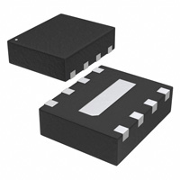


 工商网监
湘ICP备2023018690号
工商网监
湘ICP备2023018690号
