Low Capacitance 3.3 Volt TVS for High Speed Interfaces
PROTECTION PROTECTION PRODUCTS Description
The LC03-3.3 transient voltage suppressor is designed to protect components which are connected to high speed data and telecommunication lines from voltage surges caused by lightning, electrostatic discharge (ESD), and electrical fast transients (EFT). TVS diodes are ideal for use as board level protection of sensitive semiconductor components. The LC033.3 combines a TVS diode with a rectifier bridge to provide transient protection in both common and differential mode with a single device. The LC03-3.3 utilizes Semtech’s EPD technology for superior electrical characteristics at 3.3 volts. The capacitance of the device is minimized to ensure correct signal transmission on high speed lines. The LC03-3.3 meets the short-haul (intra-building) transient immunity requirements of Bellcore 1089 for telecommunications applications.
LC03-3.3
Features
1800 watts peak pulse power (tp = 8/20µs) Transient protection for high-speed data lines to Bellcore 1089 (Intra-Building) 100A (2/10µs) ITU K.20 IPP=40A (5/310µs) IEC 61000-4-2 (ESD) ±15kV (air), ±8kV (contact) IEC 61000-4-4 (EFT) 40A (5/50ns) IEC 61000-4-5 (Lightning) 100A (8/20µs) Protects two lines in common and differential mode Low capacitance for high-speed interfaces Low operating voltage (3.3V) Low clamping voltage Integrated structure saves board space and increases reliability Solid-state EPD technology
Mechanical Characteristics
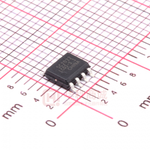
JEDEC SO-8 package RoHS/WEEE Compliant Molding compound flammability rating: UL 94V-0 Marking : Part number, date code Packaging : Tube or Tape and Reel per EIA 481
Applications
Low Voltage Interfaces T3/E3 10/100 Ethernet Set-Top Box ISDN Interfaces
Circuit Diagram
Schematic & PIN Configuration
1
8
Pin 1 and 8
2 7
Pin 2, 3, 6, and 7 Ground Pin 4 and 5
3
6
4
5
SO-8 (Top View)
Revision 01/18/2008 1 www.semtech.com
�LC03-3.3
PROTECTION PRODUCTS Absolute Maximum Rating
R ating Peak Pulse Power (tp = 8/20µs) Peak Pulse Current (tp = 8/20µs) Lead Soldering Temp erature Op erating Temp erature Storage Temp erature Symbol Pp k IP P TL TJ TSTG Value 1800 100 260 (10 sec.) -55 to +125 -55 to +150
PRELIMINARY
Units Watts A °C °C °C
Electrical Characteristics
LC03-3.3 Parameter Reverse Stand-Off Voltage Punch-Through Voltage Snap-Back Voltage Reverse Leakage Current Clamping Voltage Clamping Voltage Clamping Voltage Clamping Voltage Junction Capacitance Symbol VRWM V PT VSB IR VC VC VC VC Cj IPT = 2µA ISB = 50mA VRWM = 3.3V, T=25°C IPP = 50A, tp = 8/20µs Line-to-Ground IPP = 50A, tp = 8/20µs Line-to-Line IPP = 100A, tp = 8/20µs Line-to-Ground IPP = 100A, tp = 8/20µs Line-to-Line Between I/O pins and Ground VR = 0V, f = 1MHz Between I/O pins VR = 0V, f = 1MHz 16 3.5 2.8 1 11.5 13.5 15 18 25 Conditions Minimum Typical Maximum 3.3 Units V V V µA V V V V pF
8
12
pF
2008 Semtech Corp.
2
www.semtech.com
�LC03-3.3
PROTECTION PRODUCTS Typical Characteristics
Non-Repetitive Peak Pulse Power vs. Pulse Time
100
110 100 % of Rated Power or PP I 90 80 70 60 50 40 30 20 10 0
Power Derating Curve
Peak Pulse Power - Ppk (kW)
10
1
0.1 0.1 1 10 Pulse Duration - tp (µs) 100 1000
0
25
50
75
100
125
150
175
Ambient Temperature - TA (oC)
Pulse Waveform
110 100 90 80 Percent of IPP 70 60 50 40 30 20 10 0 0 5 10 15 Time (µs) 20 25 30 td = IPP/2 e
-t
Clamping Voltage vs. Peak Pulse Current
Waveform Parameters: tr = 8µs td = 20µs
20
Clamping Voltage - VC (V)
Line-To-Line
15
10
Line-To-Ground
5
0 0 20 40 60 Peak Pulse Current - IPP (A)
Waveform Parameters: tr = 8µs td = 20µs
80
100
Normalized Capacitance vs. Reverse Voltage
CH1 S 21 LOG
Insertion Loss S21 (Line to Ground)
3 dB/ REF 0 dB
1.4 1.2
CJ(VR) / C J(VR=0)
1 0.8 0.6 0.4 0.2
f = 1 MHz
0 0 0.5 1 1.5 2 2.5 3 3.5
Reverse Voltage - VR (V)
. S TOP 3000 000000 MHz
START. 030 M Hz
2008 Semtech Corp.
3
www.semtech.com
�LC03-3.3
PROTECTION PRODUCTS Applications Information
Device Connection Options for Protection of Two High-Speed Data Lines The LC03-3.3 is designed to protect two high-speed data lines (one differential pair) from transient overvoltages which result from lightning and ESD. The device can be configured to protect in differential (Lineto-Line) and common (Line-to-Ground) mode. Data line inputs/outputs are connected at pins 1 to 8, and 4 to 5 as shown. Pins 2, 3, 6, and 7 are connected to ground. These pins should be connected directly to a ground plane on the board for best results. The path length is kept as short as possible to minimize parasitic inductance. In applications where high common mode voltages are present, differential protection is achieved by leaving pins 2, 3, 6, and 7 not connected. Matte Tin Lead Finish Matte tin has become the industry standard lead-free replacement for SnPb lead finishes. A matte tin finish is composed of 100% tin solder with large grains. Since the solder volume on the leads is small compared to the solder paste volume that is placed on the land pattern of the PCB, the reflow profile will be determined by the requirements of the solder paste. Therefore, these devices are compatible with both lead-free and SnPb assembly techniques. In addition, unlike other lead-free compositions, matte tin does not have any added alloys that can cause degradation of the solder joint.
PRELIMINARY
Connection for Differential (Line-to-Line) and Common Mode Protection (Line-to-Ground)
Connection for Differential Protection (Line-to-Line)
2008 Semtech Corp.
4
www.semtech.com
�LC03-3.3
PROTECTION PRODUCTS Applications Information - SPICE Model
0.7 nH
D2 D1
D2
D2
D2
LC03-3.3 Spice Model
LC03-3.3 Spice Parameters Parameter IS BV VJ RS IB V CJO TT M N EG Unit Amp Volt Volt Ohm Amp Farad sec --eV D1 (T VS) 1.0E-20 3.5 13.8 0.0257 1E-3 3.4e-9 2.541E-9 0.145 1.1 1.11 D2 (LCR D) 3.98E-13 240 0.64 0.048 1E-3 8.0E-12 2.541E-9 0.022 1.1 1.11
2008 Semtech Corp.
5
www.semtech.com
�LC03-3.3
PROTECTION PRODUCTS Outline Drawing - SO-8 PRELIMINARY
A N 2X E/2 E1 E 1 ccc C 2X N/2 TIPS 2 e/2 B D aaa C SEATING PLANE A2 A C bxN bbb A1 C A-B D SIDE VIEW GAGE PLANE 0.25 e D
h h
H
DIM
c
A A1 A2 b c D E1 E e h L L1 N 01 aaa bbb ccc
DIMENSIONS INCHES MILLIMETERS MIN NOM MAX MIN NOM MAX
.053 .069 .004 .010 .049 .065 .020 .012 .007 .010 .189 .193 .197 .150 .154 .157 .236 BSC .050 BSC .010 .020 .016 .028 .041 (.041) 8 0° 8° .004 .010 .008 1.35 1.75 0.10 0.25 1.25 1.65 0.31 0.51 0.17 0.25 4.80 4.90 5.00 3.80 3.90 4.00 6.00 BSC 1.27 BSC 0.25 0.50 0.40 0.72 1.04 (1.04) 8 0° 8° 0.10 0.25 0.20
L (L1) DETAIL
01
A
SEE DETAIL
A
NOTES: 1. CONTROLLING DIMENSIONS ARE IN MILLIMETERS (ANGLES IN DEGREES). 2. DATUMS -A- AND -B- TO BE DETERMINED AT DATUM PLANE -H3. DIMENSIONS "E1" AND "D" DO NOT INCLUDE MOLD FLASH, PROTRUSIONS OR GATE BURRS. 4. REFERENCE JEDEC STD MS-012, VARIATION AA.
Land Pattern -SO-8
X
DIM
(C) G Z C G P X Y Z
DIMENSIONS INCHES MILLIMETERS
(.205) .118 .050 .024 .087 .291 (5.20) 3.00 1.27 0.60 2.20 7.40
Y P
NOTES: 1. THIS LAND PATTERN IS FOR REFERENCE PURPOSES ONLY. CONSULT YOUR MANUFACTURING GROUP TO ENSURE YOUR COMPANY'S MANUFACTURING GUIDELINES ARE MET.
2. REFERENCE IPC-SM-782A, RLP NO. 300A.
2008 Semtech Corp.
6
www.semtech.com
�LC03-3.3
PROTECTION PRODUCTS Ordering Information
Part Number LC03-3.3.TB LC03-3.3.TBT Lead Finish SnPb Pb Free Qty per Reel 500 500 R eel Size 7 Inch 7 Inch
Marking Diagram
SC YYWW LC03-3.3
Note: YYWW = Date Code
Contact Information
Semtech Corporation Protection Products Division 200 Flynn Road, Camarillo, CA 93012 Phone: (805)498-2111 FAX (805)498-3804
2008 Semtech Corp. 7 www.semtech.com
�
很抱歉,暂时无法提供与“LC03-3.3.TBT”相匹配的价格&库存,您可以联系我们找货
免费人工找货- 国内价格
- 1+4.50587
- 30+4.3505
- 100+4.03975
- 500+3.729
- 1000+3.57362