PROTECTION PRODUCTS - RailClamp® PROTECTION Description
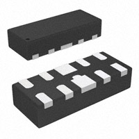
RailClamps® are ultra low capacitance TVS arrays designed to protect high speed data interfaces. This series has been specifically designed to protect sensitive components which are connected to high-speed data and transmission lines from overvoltage caused by ESD (electrostatic discharge), CDE (Cable Discharge Events), and EFT (electrical fast transients). The RClampTM0524J has a typical capacitance of only 0.30pF between I/O pins. This allows it to be used on circuits operating in excess of 3GHz without signal attenuation. They may be used to meet the ESD immunity requirements of IEC 61000-4-2, Level 4 (±15kV air, ±8kV contact discharge). Each device is designed to protect four lines (two differential pairs). The RClamp0524J is in a 8-pin, RoHS/WEEE compliant, SLP2710P8 package. It measures 2.7 x 1.0 x 0.58mm. The leads are spaced at a pitch of 0.5mm and are finished with lead-free NiPdAu. They are designed for easy PCB layout by allowing the traces to run straight through the device. The combination of small size, low capacitance, and high level of ESD protection makes them a flexible solution for applications such as HDMI, DisplayPortTM, MDDI, and eSATA interfaces.
RailClamp® Ultra Low Capacitance TVS Arrays
PRELIMINARY Features
ESD protection for high-speed data lines to IEC 61000-4-2 (ESD) ±15kV (air), ±8kV (contact) IEC 61000-4-5 (Lightning) 5A (8/20μs) IEC 61000-4-4 (EFT) 40A (5/50ns) Package design optimized for high speed lines Flow-Through design Protects four I/O lines Low capacitance: 0.3pF typical (I/O to I/O) Low clamping voltage Low operating voltage: 5V Solid-state silicon-avalanche technology
RClamp0524J
Mechanical Characteristics
SLP2710P8 8-pin package (2.7 x 1.0 x 0.58mm) RoHS/WEEE Compliant Lead Pitch: 0.5mm Lead finish: NiPdAu Marking: Marking Code Packaging: Tape and Reel per EIA 481
Applications
High Definition Multi-Media Interface (HDMI) Digital Visual Interface (DVI) DisplayPortTM Interface MDDI Ports LVDS Serial ATA PCI Express
Dimensions
2.70 0.40
Circuit Diagram
1
2
1.00
0.60 0.20 0.50
Pin 1
Pin 2
Pin 3
Pin 4
0.58
GND
Nominal Dimensions in mm
Revision 02/05/2008 1
4-Line Protection
www.semtech.com
�RClamp0524J
PROTECTION PRODUCTS Absolute Maximum Rating
Rating Peak Pulse Power (tp = 8/20μs) Peak Pulse Current (tp = 8/20μs) ESD per IEC 61000-4-2 (Air) ESD per IEC 61000-4-2 (Contact) Operating Temperature Storage Temperature Symbol Ppk IPP VESD TJ TSTG Value 150 5 +/- 17 +/- 12 -55 to +125 -55 to +150
PRELIMINARY
Units Watts A kV °C °C
Electrical Characteristics (T=25oC)
Parameter Reverse Stand-Off Voltage Reverse Breakdown Voltage Reverse Leakage Current Clamping Voltage Symbol VRWM V BR IR VC Conditions Any I/O pin to ground It = 1mA Any I/O pin to ground VRWM = 5V, T=25°C Any I/O pin to ground IPP = 1A, tp = 8/20μs Any I/O pin to ground VR = 0V, f = 1MHz Between I/O pins VR = 0V, f = 1MHz Any I/O pin to ground 0.30 6 1 15 0.4 0.8 Minimum Typical Maximum 5 Units V V μA V pF pF
Junction Capacitance Junction Capacitance
Cj Cj
© 2008 Semtech Corp.
2
www.semtech.com
�RClamp0524J
PROTECTION PRODUCTS Typical Characteristics
Non-Repetitive Peak Pulse Power vs. Pulse Time
10
110 100
PRELIMINARY
Power Derating Curve
Peak Pulse Power - PPP (kW)
% of Rated Power or IPP
90 80 70 60 50 40 30 20 10
1
0.1
0.01 0.1 1 10 Pulse Duration - tp (us) 100 1000
0 0 25 50 75 100 125 150 Ambient Temperature - TA (oC)
Pulse Waveform
110 100 90 80 70 60 50 40 30 20 10 0 0 5 10 15 Time (µs) 20 25 30 td = IPP/2
PP
Clamping Voltage vs. Peak Pulse Current
Waveform Parameters: tr = 8µs td = 20µs
40 35 Clamping Voltage -VC (V) 30 25 20 15 10 5 0 0 1 2 3 4 5 6 Peak Pulse Current - IPP (A) Waveform Parameters: tr = 8µs td = 20µs
Line to Gnd Line to Line
Percent of I
e-t
Normalized Capacitance vs. Reverse Voltage
1.5 1.4 1.3 1.2 1.1 1 0.9 0.8 0.7 0.6 0.5 0.4 0.3 0.2 0.1 0 0 1 2 3 Reverse Voltage - VR (V) 4
ESD Clamping for +8kV pulse per IEC 61000-4-2
CJ(VR) / CJ(VR=0)
f = 1 MHz 5
© 2008 Semtech Corp.
3
www.semtech.com
�RClamp0524J
PROTECTION PRODUCTS Typical Characteristics (Con’t)
Insertion Loss S21 - I/O to I/O
CH1 S21 LOG 6 dB / REF 0 dB 1: -0.076 dB 900 MHz
3
PRELIMINARY
Insertion Loss S21 - I/O to GND
CH1 S21 LOG 6 dB / REF 0 dB 1: -0.086 dB 900 MHz
3
0 dB
1 2
2: -0.062 dB 1.8 GHz 3: -0.1087 dB 2.5 GHz
0 dB
1 2
2: -0.0336 dB 1.8 GHz 3: -0.126 dB 2.5 GHz
-6 dB -12 dB -18 dB -24 dB -30 dB -36 dB -42 dB -48 dB 1 MHz START . 030 MHz 10 MHz 100 MHz
-6 dB -12 dB -18 dB -24 dB -30 dB -36 dB -42 dB -48 dB 1 MHz START . 030 MHz 10 MHz 100 MHz
3 1 GHz GHz STOP 3000. 000000 M Hz
3 1 GHz GHz STOP 3000. 000000 M Hz
© 2008 Semtech Corp.
4
www.semtech.com
�RClamp0524J
PROTECTION PRODUCTS Applications Information
Design Recommendations for HDMI Protection Adding external ESD protection to HDMI ports can be challenging. First ESD protection devices have an inherent junction capacitance. However, adding even a small amount of capacitance will cause the impedance of the differential pair to drop. Second, large packages and land pattern requirements cause discontinuities that adversely affect signal integrity. The RClamp0524J is specifically designed for protection of high-speed interfaces such as HDMI. They present ±8kV ESD contact discharges (>±15kV air discharge) as outlined in IEC 61000-4-2. Each device is in a leadless SLP package that is less than 1.1mm wide. They are designed such that the traces flow straight through the device. The narrow package and flow-through design reduces discontinuities and minimizes impact on signal integrity. This becomes even more critical as signal speeds increase. Pin Configuration Figure 1 is an example of how to route the high speed differential traces through the RClamp0524J. The solid line represents the PCB trace. The PCB traces are used to connect the pin pairs for each line (pin 1 to pin 8, pin 2 to pin 7, pin 3 to pin 6, pin 4 to pin 5). For example, line 1 enters at pin 1 and exits at Pin 8 and the PCB trace connects pin 1 and 8 together. This is true for lines connected at pins 2, 3, and 4 also. Ground is connected at the center tabs. One large ground pad should be used in lieu of two separate pads. TDR Measurements for HDMI The combination of low capacitance, small package, and flow-through design means it is possible to use these devices to meet the HDMI impedance requirements of 100 Ohm ±15% without any PCB board modification. Figures 3 and 4 show impedance test results for a TDR risetime of 200ps and 100ps respectively, using a Semtech evaluation board with 100 Ohm traces throughout. Measurements were taken using a TDR method as outlined in the HDMI Compliance Test Specification (CTS). In each case, the device meets the HDMI CTS
PRELIMINARY
8 7 GND 6 5
1
Pin 1, 2, 3, 4 5, 6, 7, 8 GN D
2
GND
3
4
Identification Inp ut Lines Outp ut Lines (N o Internal Connection) Ground
SLP2710P8 Pin Configuration (Top View)
12 11 10
1
HDMI Connector
GND
9 8 7
GND
1
6 5 4
GND
3 2 1
GND
Figure 1. Flow through Layout Using Clamp052 p0524J R Clam p052 4J
© 2008 Semtech Corp.
5
www.semtech.com
�RClamp0524J
PROTECTION PRODUCTS Applications Information
requirement of 100 Ohm ±15% with plenty of margin. For signal integrity purposes, the best results will be obtained by using the RClamp0524J to protect the high-speed differential pairs. This is because the device is designed such that the data lines from the connector line up with the I/O pins of the device without altering the trace routing. Either the RClamp0504P or RClamp0524J may be used to protect the remaining lines (I2C, CEC, and hot plug) depending on layout constraints. Layout Guidelines for Optimum ESD Protection Good circuit board layout is critical not only for signal integrity, but also for effective suppression of ESD induced transients. For optimum ESD protection, the following guidelines are recommended: Place the device as close to the connector as possible. This practice restricts ESD coupling into adjacent traces and reduces parasitic inductance. The ESD transient return path to ground should be kept as short as possible. Whenever possible, use multiple micro vias connected directly from the device ground pad to the ground plane. Avoid running critical signals near board edges.
PRELIMINARY
B
A
X-axis Y-axis
A 1.905 101.0
B 2.081 107.0
(nsec) (Ohm)
Figure 2 - TDR Measurement with 200ps risetime using Semtech Evaluation Board
B
A
X-axis Y-axis
A 1.80 96
B 2.076 108.0
(nsec) (Ohm)
Figure 3 - TDR Measurement with 100ps risetime using Semtech Evaluation Board
Note: Measurements were taken on SLP HDMI EVAL Rev C Board that has 100Ω differential traces impedance throughout (No trace Compensation).
© 2008 Semtech Corp.
6
www.semtech.com
�RClamp0524J
PROTECTION PRODUCTS Applications Information PRELIMINARY
RClamp0524J
Data 2+ Data 2Data 1+ Data 1Data 0+ Data 0Clk+ Clk-
To HDMI Graphics Chip
RClamp0524J
CEC SCL SDA Gnd 5VPower HP Detect
1 6
RClamp0504P
Figure 4. HDMI Protection Example
ESATA Host Plug Host Plug Host Plug
Host Tx + Host Tx -
A+ A-
Host Rx Host Rx +
B-
1 RClamp0524J
B+
A+ A-
1
ESATA Device Plug
BB+ -
RClamp0524J
eSAT Pro Example Figure 5. eSATA Pr o t ection Exam ple
© 2008 Semtech Corp. 7 www.semtech.com
�RClamp0524J
PROTECTION PRODUCTS Applications Information PRELIMINARY
1 RClamp0524J
DISPLAY PORT CONNECTOR
1 RClamp0524J
Ohm
μ
1 RClamp0524J
DisplayPort Pro yPor Example Figure 6. DisplayPor t Prot ection Example
© 2008 Semtech Corp.
8
www.semtech.com
�RClamp0524J
PROTECTION PRODUCTS Applications Information Spice Model PRELIMINARY
RClamp0524J Spice Model
R Clamp0524J Spice Parameters Parameter IS BV VJ RS IB V CJO TT M N EG Unit Amp Volt Volt Ohm A mp Farad sec --eV D1 (LCR D) 1E-20 100 0.7 0.458 1E-3 0.4E-12 2.541E-9 0.01 1.1 1.11 D2 (LCR D) 1E-20 100 0.7 1.0 1E-3 0.6E-12 2.541E-9 0.01 1.1 1.11 D3 (T VS) 2E-12 9.36 0.6 2.6 1E-3 56E-12 2.541E-9 0.23 1.1 1.11
www.semtech.com
© 2008 Semtech Corp.
9
�RClamp0524J
PROTECTION PRODUCTS Outline Outline Drawing - SO-8 SLP2710P8
A D B
PRELIMINARY
DIM
PIN 1 INDICATOR (LASER MARK) E
A A1 A2 b b1 D E e e1 L N aaa bbb
A aaa C A2 R0.125 1 E/2 LxN 2 A1 b1xN bbb C
SEATING PLANE
DIMENSIONS INCHES MILLIMETERS MIN NOM MAX MIN NOM MAX .020 .023 .026 0.50 0.58 0.65 0.00 .001 .002 0.00 0.03 0.05 (.005) (0.13) .006 .008 .010 0.15 0.20 0.25 .014 .016 .018 0.35 0.40 0.45 .102 .106 .110 2.60 2.70 2.80 .035 .039 .043 0.90 1.00 1.10 .020 BSC 0.50 BSC .024 BSC 0.60 BSC .012 .015 .017 0.30 0.38 0.425 10 10 .003 0.08 .004 0.10
CAB
N e1
2X R0.075 7 PLACES bxN e bbb CAB
D/2 NOTES: 1. CONTROLLING DIMENSIONS ARE IN MILLIMETERS (ANGLES IN DEGREES).
Land Pattern - SLP2710P8
P1 P
DIMENSIONS DIM C G P P1 X X1 Y Y1 Z INCHES (.034) .008 .020 .024 .008 .016 .027 (.061) .061 MILLIMETERS (0.875) 0.20 0.50 0.60 0.20 0.40 0.675 (1.55) 1.55
Y Z (C) G (Y1)
X X1
NOTES:
1. CONTROLLING DIMENSIONS ARE IN MILLIMETERS (ANGLES IN DEGREES). 2. THIS LAND PATTERN IS FOR REFERENCE PURPOSES ONLY. CONSULT YOUR MANUFACTURING GROUP TO ENSURE YOUR COMPANY'S MANUFACTURING GUIDELINES ARE MET.
© 2008 Semtech Corp.
10
www.semtech.com
�RClamp0524J
PROTECTION PRODUCTS Marking Codes Ordering Information
Part Number
PRELIMINARY
PIN 1 INDICATOR
YYWW = Date Code
0524J
YYWW
Number of Lines
Qty per Reel
Reel Size 7 Inch
RClamp0524J.TCT
4
3000
Note: Lead finish is lead-free NiPdAu.
Tape and Reel Specification
Pin 1 Location
User Direction of feed
Device Orientation in Tape
Part Number RClamp 0524J
Tape Width
A0 1.21 +/-0.10 mm
B0 2.91 +/-0.10 mm
K0 0.66 +/-0.10 mm
K (MAX)
B, (Max)
D
D1
E
F
P
P0
P2
T(MAX)
W 8.0 mm + 0.3 mm - 0.1 mm
8 mm
4.2 mm
1.5 + 0.1 mm - 0.0 mm )
0.5 mm ±0.05
1.750±.10 mm
3.5±0.05 mm
2.4 mm
4.0±0.1 mm
4.0±0.1 mm
2.0±0.05 mm
0.4 mm
Contact Information
Semtech Corporation Protection Products Division 200 Flynn Road, Camarillo, CA 93012 Phone: (805)498-2111 FAX (805)498-3804
© 2008 Semtech Corp. 11 www.semtech.com
�
很抱歉,暂时无法提供与“RCLAMP0524J.TCT”相匹配的价格&库存,您可以联系我们找货
免费人工找货