0
登录后你可以
  • 下载海量资料
  • 学习在线课程
  • 观看技术视频
  • 写文章/发帖/加入社区
会员中心
创作中心
发布
  • 发文章

  • 发资料

  • 发帖

  • 提问

  • 发视频

创作活动
UCLAMP0505A.TCT

UCLAMP0505A.TCT

  • 厂商:

    SEMTECH

  • 封装:

  • 描述:

    UCLAMP0505A.TCT - μClampTM 5-Line ESD protection Array - Semtech Corporation

  • 详情介绍
  • 数据手册
  • 价格&库存
UCLAMP0505A.TCT 数据手册
µClampTM 5-Line ESD protection Array PROTECTION PROTECTION PRODUCTS - MicroClampTM Description The µClampTM series of TVS arrays are designed to protect sensitive electronics from damage or latch-up due to ESD. They are designed for use in applications where board space is at a premium. Each device requires less than 2.9mm2 of PCB area and will protect up to five lines. They are unidirectional devices and may be used on lines where the signal polarities are above ground. TVS diodes are solid-state devices designed specifically for transient suppression. They feature large cross-sectional area junctions for conducting high transient currents. They offer desirable characteristics for board level protection including fast response time, low operating and clamping voltage, and no device degradation. The uClampTM0505A may be used to meet the immunity requirements of IEC 61000-4-2, level 4. The small SC89 package makes them ideal for use in portable electronics such as cell phones, PDA’s, notebook computers, and digital cameras. These devices feature a lead-free, matte tin lead finish. They are compatible with both lead free and SnPb assembly techniques. uClamp0505A Features Transient protection for data lines to IEC 61000-4-2 (ESD) ±15kV (air), ±8kV (contact) IEC 61000-4-4 (EFT) 40A (5/50ns) Protects five I/O lines Ultra-small SC-89 package (1.7 x 1.7 x 0.6mm 0.6mm) 1.7 2 requires less than 2.9mm of PCB area Working voltage: 5V Low leakage current Low operating and clamping voltages Solid-state silicon-avalanche technology Mechanical Characteristics SC-89 (SOT-666) package Molding compound flammability rating: UL 94V-0 Marking : Marking Code and pin 1 indicator Weight: 2.9mg (typical) Lead Finish: Matte Tin Packaging : Tape and Reel per EIA 481 Applications Cellular Handsets & Accessories Cordless Phones Personal Digital Assistants (PDA’s) Notebooks & Handhelds Portable Instrumentation Digital Cameras Peripherals MP3 Players Dimensions 1.70 0.50 Schematic & PIN Configuration 1.25 1.70 0.30 0.60 Maximum Dimensions (mm) Revision 06/23/04 1 SC-89 (Top View) www.semtech.com uClamp0505A PROTECTION PRODUCTS Absolute Maximum Rating R ating Peak Pulse Power (tp = 8/20µs) Maximum Peak Pulse Current ( tp = 8/20µs) ESD per IEC 61000-4-2 (Air) ESD per IEC 61000-4-2 (Contact) Lead Soldering Temperature Operating Temperature Storage Temperature Symbol Pp k Ip p V PP TL TJ TSTG Value 100 7 +/- 20 +/- 12 260 (10 sec.) -55 to +125 -55 to +150 Units Watts Amps kV °C °C °C Electrical Characteristics (T=25oC) Parameter Reverse Stand-Off Voltage Reverse Breakdown Voltage Reverse Leakage Current Reverse Leakage Current Forward Voltage Clamping Voltage Clamping Voltage Junction Capacitance Symbol VRWM V BR IR IR VF VC VC Cj It = 1mA VRWM = 5V, T=25°C VRWM = 3V, T=25°C IF = 10mA IPP = 1A, tp = 8/20µs IPP = 7A, tp = 8/20µs Between I/O Pins and Gnd VR = 0V, f = 1MHz 60 0.80 10 12 75 6 1 0.500 Conditions Minimum Typical Maximum 5 Units V V µA µA V V V pF  2004 Semtech Corp. 2 www.semtech.com uClamp0505A PROTECTION PRODUCTS Typical Characteristics Non-Repetitive Peak Pulse Power vs. Pulse Time 10 Power Derating Curve 110 100 90 % of Rated Power or I PP 80 70 60 50 40 30 20 10 0 Peak Pulse Power - P PP (kW) 1 0.1 0.01 0.1 1 10 Pulse Duration - tp (µs) 100 1000 0 25 50 75 100 125 150 Ambient Temperature - TA (oC) Clamping Voltage vs. Peak Pulse Current 12 10 Forward Voltage - VF (V) 6 8 6 4 2 0 0 1 2 3 4 5 6 7 8 Peak Pulse Current - Ipp (A) 8 Forward Voltage vs. Forward Current Clamping Voltage - Vc (V) 4 Waveform Parameters: tr = 8us td = 20us 2 Waveform Parameters: tr = 8us td = 20us 0 5 10 Forward Current - IF (A) 15 0 Junction Capacitance vs. Reverse Voltage 60 CH1 S21 LOG Insertion Loss S21 6 dB / REF 0 dB Capacitance - Cj (pF) 50 40 30 20 0 1 2 3 Reverse Voltage - VR (V) 4 5 START. 030 MHz STOP 3000. 000000 MHz  2004 Semtech Corp. 3 www.semtech.com uClamp0505A PROTECTION PRODUCTS Typical Characteristics (Con’t.) ESD Clamping (8kV Contact per IEC 61000-4-2) ESD Clamping (-8kV Contact per IEC 61000-4-2) ESD Clamping (15kV air per IEC 61000-4-2) ESD Clamping (-15kV air per IEC 61000-4-2)  2004 Semtech Corp. 4 www.semtech.com uClamp0505A PROTECTION PRODUCTS Applications Information Device Connection for Protection of Five Data Lines These devices are designed to protect up to five unidirectional data lines. The device is connected as follows: 1. Unidirectional protection of five I/O lines is achieved by connecting pins 1, 3, 4, 5, and 6 to the data lines. Pin 2 is connected to ground. The ground connection should be made directly to the ground plane for best results. The path length is kept as short as possible to reduce the effects of parasitic inductance in the board traces. Circuit Board Layout Recommendations for Suppression of ESD. Good circuit board layout is critical for the suppression of ESD induced transients. The following guidelines are recommended: Place the TVS near the input terminals or connectors to restrict transient coupling. Minimize the path length between the TVS and the protected line. Minimize all conductive loops including power and ground loops. The ESD transient return path to ground should be kept as short as possible. Never run critical signals near board edges. Use ground planes whenever possible. Matte Tin Lead Finish Matte tin has become the industry standard lead-free replacement for SnPb lead finishes. A matte tin finish is composed of 100% tin solder with large grains. Since the solder volume on the leads is small compared to the solder paste volume that is placed on the land pattern of the PCB, the reflow profile will be determined by the requirements of the solder paste. Therefore, these devices are compatible with both lead-free and SnPb assembly techniques. In addition, unlike other lead-free compositions, matte tin does not have any added alloys that can cause degradation of the solder joint. 2 1 3 Circuit Diagram 4 5 6 Protection of Five Unidirectional Lines  2004 Semtech Corp. 5 www.semtech.com uClamp0505A PROTECTION PRODUCTS Typical Applications uClamp0505A  2004 Semtech Corp. 6 www.semtech.com uClamp0505A PROTECTION PRODUCTS Outline Drawing - SC-89 (SOT-666) D A N E /2 E1 E D L 1 e N xb B aaa C A -B D 2 c A D IM C L1 A b c D E E1 e L L1 N aaa D IM E N S IO N S IN C H E S M IL L IM E T E R S M IN N O M M A X M IN N O M M A X .0 1 9 .0 0 5 .0 0 3 .0 5 9 .0 6 1 .0 4 3 .0 2 4 .0 1 2 .0 0 7 .0 6 7 .0 6 7 .0 4 9 0 .5 0 0 .1 5 0 .1 0 1 .5 0 1 .5 5 1 .1 0 0 .6 0 0 .3 0 0 .1 8 1 .7 0 1 .7 0 1 .2 5 .0 6 3 .0 6 3 .0 4 7 .0 2 0 B S C .0 0 3 .0 1 2 .0 0 8 .0 0 3 .0 0 6 .0 0 8 6 .0 0 4 1 .6 0 1 .6 0 1 .2 0 0 .5 0 B S C 0 .1 0 0 .3 0 0 .2 0 0 .1 0 0 .1 5 0 .2 0 6 0 .1 0 NO TES: 1. 2. C O N T R O L L IN G D IM E N S IO N S A R E IN M IL L IM E T E R S (A N G L E S IN D E G R E E S ). D IM E N S IO N S "E 1 " A N D " D " D O N O T IN C L U D E M O L D F L A S H , P R O T R U S IO N S OR G ATE BURRS. Land Pattern - SC-89 (SOT-666) X Y C DIM C P G X Y Z DIMENSIONS INCHES MILLIMETERS (.057) .020 .024 .012 .033 .090 (1.45) 0.50 0.60 0.30 0.85 2.30 Z G Y P NOTES: 1. THIS LAND PATTERN IS FOR REFERENCE PURPOSES ONLY CONSULT YOUR MANUFACTURING GROUP TO ENSURE YOUR COMPANY'S MANUFACTURING GUIDELINES ARE MET.  2004 Semtech Corp. 7 www.semtech.com uClamp0505A PROTECTION PRODUCTS Marking Code Ordering Information Part Number uClamp 0505A.TCT Working Voltage 5V Device Qty per Marking Reel B 3,000 Reel Size 7 Inch B Note: (1) Pin 1 Identified with a dot (2) Lead finish is matte tin MicroClamp, uClamp and µClamp are trademarks of Semtech Corporation Tape and Reel Specification B B B Tape Specification and Device Orientation Contact Information Semtech Corporation Protection Products Division 200 Flynn Rd., Camarillo, CA 93012 Phone: (805)498-2111 FAX (805)498-3804 www.semtech.com  2004 Semtech Corp. 8
UCLAMP0505A.TCT
物料型号: - 型号:uClamp0505A - 工作电压:5V - 器件标记:B - 每卷数量:3000 - 卷径:7英寸

器件简介: - uClamp0505A属于MicroClamp™系列TVS阵列,专为保护敏感电子设备免受ESD损害或锁定而设计。该设备适用于板空间有限的应用场合,每个器件占用的PCB面积不到2.9平方毫米,并且可以保护多达五条线路。它们是单向设备,可以用于信号极性高于地线的线路上。TVS二极管是专为瞬态抑制而设计固态设备,具有大的横截面积结,可传导高瞬态电流。它们提供了板级保护所需的理想特性,包括快速响应时间、低工作和钳位电压以及无设备退化。uClamp0505A可用于满足IEC 61000-4-2,4级免疫要求。小SC89封装使它们非常适合用于便携电子设备,如手机、PDA、笔记本电脑和数字相机。这些设备具有无铅、亚光锡铅表面处理。它们兼容无铅和SnPb组装技术。

引脚分配: - 引脚1、3、4、5、6连接到数据线,引脚2连接到地。

参数特性: - 传输保护:符合IEC 61000-4-2 (ESD) ±15kV(空气),±8kV(接触)IEC 61000-4-4 (EFT) 40A(5/50ns) - 保护五条I/O线路 - 工作电压:5V - 低漏电流 - 低操作和钳位电压 - 固态硅雪崩技术

功能详解: - uClamp0505A提供五条I/O线路的单向保护,通过将引脚1、3、4、5、6连接到数据线,引脚2连接到地来实现。为了获得最佳效果,地连接应直接连接到地平面,路径长度应尽可能短,以减少PCB走线中寄生电感的影响。

应用信息: - 适用于手机及配件、无绳电话、个人数字助理(PDA)、笔记本电脑和手持设备、便携式仪器、数字相机、外围设备、MP3播放器等。
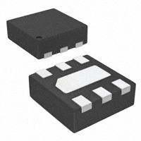
封装信息: - 封装类型:SC-89 (SOT-666) - 封装尺寸:1.7 x 1.7 x 0.6mm - 重量:2.9mg(典型值) - 引脚表面处理:亚光锡 - 包装:符合EIA 481标准的带和卷
UCLAMP0505A.TCT 价格&库存

很抱歉,暂时无法提供与“UCLAMP0505A.TCT”相匹配的价格&库存,您可以联系我们找货

免费人工找货