Low Voltage μClampTM for ESD and CDE Protection
PROTECTION PROTECTION PRODUCTS - MicroClampTM Description
The μClamp series of Transient Voltage Suppressors (TVS) are designed to replace multilayer varistors (MLVs) in portable applications such as cell phones, notebook computers, and PDAs. They offer superior electrical characteristics such as lower clamping voltage and no device degradation when compared to MLVs. They are designed to protect sensitive semiconductor components from damage or upset due to electrostatic discharge (ESD), lightning, electrical fast transients (EFT), and cable discharge events (CDE). The μClampTM3301H is constructed using Semtech’s proprietary EPD process technology. The EPD process provides low standoff voltages with significant reductions in leakage currents and capacitance over siliconavalanche diode processes. They feature a true operating voltage of 3.3 volts for superior protection when compared to traditional pn junction devices. The μClamp3301H is in a SOD-523 package and will protect one unidirectional line. They give the designer the flexibility to protect one line in applications where arrays are not practical. They may be used to meet the ESD immunity requirements of IEC 61000-4-2, Level 4 (±15kV air, ±8kV contact discharge).
TM
uClamp3301H
Features
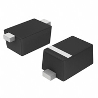
Transient protection for data lines to IEC 61000-4-2 (ESD) ±20kV (air), ±10kV (contact) IEC 61000-4-4 (EFT) 40A (tp = 5/50ns) Cable Discharge Event (CDE) Ultra-small SOD-523 package (1.7 x 0.9 x 0.7mm) Protects one I/O or power line Low clamping voltage Working voltage: 3.3V Low leakage current Solid-state silicon-avalanche technology
Mechanical Characteristics
EIAJ SOD-523 package Molding compound flammability rating: UL 94V-0 Marking : Marking code, cathode band Packaging: Tape and Reel Lead Finish: Matte tin
Applications
Cellular Handsets & Accessories Cordless Phones Personal Digital Assistants (PDAs) Notebooks & Handhelds Portable Instrumentation Digital Cameras Peripherals MP3 Players
Dimensions
1.70 1.30 0.9
Schematic & PIN Configuration
0.35
0.70
Maximum Dimensions (mm)
Revision 2/21/2008 1
SOD-523 (Top View)
www.semtech.com
�uClamp3301H
PROTECTION PRODUCTS Absolute Maximum Rating
R ating Peak Pulse Power (tp = 8/20μs) Maximum Peak Pulse Current (tp = 8/20μs) ESD per IEC 61000-4-2 (Air) ESD per IEC 61000-4-2 (Contact) Lead Soldering Temperature Operating Temperature Storage Temperature Symbol Pp k Ip p V PP TL TJ TSTG Value 40 5 +/- 20 +/- 15 260 (10 sec.) -55 to +125 -55 to +150 Units Watts Amps kV °C °C °C
Electrical Characteristics (T=25oC)
Parameter Reverse Stand-Off Voltage Punch-Through Voltage Snap -Back Voltage Reverse Leakage Current Clamp ing Voltage Clamp ing Voltage Forward Voltage Junction Cap acitance Symbol VRWM V PT VSB IR VC VC VF Cj IPT = 2μA ISB = 50mA VRWM = 3.3V IPP = 1A, tp = 8/20μs IPP = 5A, tp = 8/20μs IPP = 1A, tp = 8/20μs I/O p in to Gnd VR = 0V, f = 1MHz I/O p in to Gnd VR = 3.3V, f = 1MHz 25 3.5 2.8 0.05 0.5 5.5 8.0 2.4 30 3.9 Conditions Minimum Typical Maximum 3.3 4.6 Units V V V μA V V V pF
14
pF
© 2008 Semtech Corp.
2
www.semtech.com
�uClamp3301H
PROTECTION PRODUCTS Typical Characteristics
Non-Repetitive Peak Pulse Power vs. Pulse Time
1
110 100 90 % of Rated Power or I PP 80 70 60 50 40 30 20 10 0
Power Derating Curve
Peak Pulse Power - P PP (kW)
0.1
0.01 0.1 1 10 Pulse Duration - tp (µs) 100 1000
0
25
50
75
100
125
150
Ambient Temperature - TA (oC)
Clamping Voltage vs. Peak Pulse Current
12 10 8 6 4 2 0 0 1 2 3 4 5 Waveform Parameters: tr = 8μs td = 20μs
Junction Capacitance vs. Reverse Voltage
1.2 f = 1 MHz 1 Cj(VR) / Cj(VR=0V) 0.8 0.6 0.4 0.2 0 0 0.5 1 1.5 2 2.5 Reverse Voltage - VR (V) 3 3.5
Clamping Voltage - VC (V)
Peak Pulse Current - IPP (A)
Insertion Loss S21
CH1 S21 LOG 6 dB / REF 0 dB
ESD Clamping (8kV Contact per IEC 61000-4-2)
START . 030 M Hz
STOP 3000. 000000 M Hz
Note: Data is taken with a 10x attenuator 3 www.semtech.com
© 2008 Semtech Corp.
�uClamp3301H
PROTECTION PRODUCTS Applications Information
Device Connection Options The μClamp3301H is designed to protect one I/O, or power supply line. It will present a high impedance to the protected line up to 3.3 volts. It will “turn on” when the line voltage exceeds 3.5 volts. The device is unidirectional and may be used on lines where the signal polarity is above ground. The cathode band should be placed towards the line that is to be protected. Due to the “snap-back” characteristics of the low voltage TVS, it is not recommended that the I/O line be directly connected to a DC source greater than snapback votlage (VSB) as the device can latch on as described below. EPD TVS Characteristics The μClamp3301H is constructed using Semtech’s proprietary EPD technology. The structure of the EPD TVS is vastly different from the traditional pn-junction devices. At voltages below 5V, high leakage current and junction capacitance render conventional avalanche technology impractical for most applications. However, by utilizing the EPD technology, the μClamp3301H can effectively operate at 3.3V while maintaining excellent electrical characteristics. EPD TVS IV Characteristic Curve
IPP
Device Schematic & Pin Configuration
ISB
IPT VF IR VRWM V VPT VC SB
The EPD TVS employs a complex nppn structure in I contrast to the pn structure normally found in traditional silicon-avalanche TVS diodes. Since the EPD TVS devices use a 4-layer structure, they exhibit a slightly different IV characteristic curve when compared to conventional devices. During normal operation, the device represents a high-impedance to the circuit up to the device working voltage (VRWM). During an ESD event, the device will begin to conduct and will enter a low impedance state when the punch through voltage (VPT) is exceeded. Unlike a conventional device, the low voltage TVS will exhibit a slight negative resistance characteristic as it conducts current. This characteristic aids in lowering the clamping voltage of the device, current (ISB). To return to a non-conducting state, the but must be considered in applications where DC current through the device must fall below the ISB voltages are present. (approximately
很抱歉,暂时无法提供与“UCLAMP3301H.TCT”相匹配的价格&库存,您可以联系我们找货
免费人工找货