SGM811 SGM812
GENERAL DESCRIPTION
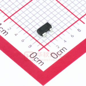
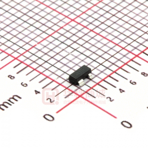
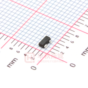
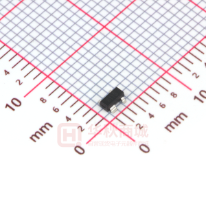
The SGM811/SGM812 supervisory circuits monitor the power supply voltage in microprocessor and digital systems. The SGM811/SGM812 is designed to monitor seven different voltages, these voltages have been selected for the effective monitoring of 2.5V, 3 V, 3.3 V, and 5 V supply voltage levels. They provide a reset output during power-up, power-down and brownout conditions. On power-up, an internal timer holds reset asserted for 240 ms. This holds the microprocessor in a reset state until conditions have stabilized. The RESET output remains operational with VCC as low as 1 V. The SGM811 provides an active low reset signal ( RESET ) while the SGM812 provides an active high signal (RESET) output. The SGM811/SGM812 has a manual reset input. The manual reset function is very useful, especially if the circuit in which the SGM811/SGM812 is operating enters into a state that can only be detected by the user. Allowing the user to reset a system manually can reduce the damage or danger that could otherwise be caused by an out-of-control or locked system. The devices come in a 4-pin SOT143 and 5-pin SOT23 packages.
Microprocessor Supervisory with Manual Reset Input
FEATURES
− Superior Upgrade for MAX811/MAX812 and ADM811/ADM812 − Specified over Temperature − Low Power Consumption (17 μA Typ) − Precision Voltage Monitor: 2.5V,3 V, 3.3 V, 5 V Options − Reset Assertion Down to 1 V VCC − 160 ms Min Power-On Reset Logic Low RESET Output (SGM811) Logic High RESET Output (SGM812) − Manual Reset Input − Compact 4-Pin SOT143 and 5-Pin SOT23 Packages
PIN CONFIGURATIONS(TOP VIEW)
SOT143-4 GND 1 4 VCC
RESET/RESET
2
3
MR
APPLICATIONS
Microprocessor Systems Controllers Intelligent Instruments Automotive Systems Safety Systems Portable Instruments
SOT23-5 GND NC RESET/RESET 1 2 3 4 MR 5 VCC
TYPICAL OPERATION CIRCUIT
VCC VCC MICROPROCESSOR SYSTEM RESET 100KO GND GND
SGM811
RESET
MR
Shengbang Microelectronics Co, Ltd Tel: 86/451/84348461 www.sg-micro.com
Nov 2006
�ORDERING INFORMATION
ORDERING NUMBER SGM811-LXN5 SGM811-M XN5 SGM811-JXN5 SGM811-T XN5 SGM811-S XN5 SGM811-R XN5 SGM811-Z XN5 SGM811-LXKA4 SGM811-MX KA4 SGM811-JX KA4 SGM811-TX KA4 SGM811-SX KA4 SGM811-RX KA4 SGM811-Z X KA4 SGM812-LXN5 SGM812-M XN5 SGM812-JXN5 SGM812-T XN5 SGM812-S XN5 SGM812-R XN5 SGM812-Z XN5 SGM812-LX KA4 SGM812-MX KA4 SGM812-JX KA4 SGM812-TX KA4 SGM812-SX KA4 SGM812-RX KA4 SGM812-Z X KA4 RESET THRESHOLD (V) 4.63 4.38 4.00 3.08 2.93 2.63 2.32 4.63 4.38 4.00 3.08 2.93 2.63 2.32 4.63 4.38 4.00 3.08 2.93 2.63 2.32 4.63 4.38 4.00 3.08 2.93 2.63 2.32 PECKAGE TYPE SPECIFIED TEMPERATURE RANGE PACKAGE MARKING 811L 811M 811J 811T 811S 811R 811Z 811L 811M 811J 811T 811S 811R 811Z 812L 812M 812J 812T 812S 812R 812Z 812L 812M 812J 812T 812S 812R 812Z PACKAGE OPTION
SOT23-5 SOT23-5 SOT23-5 SOT23-5 SOT23-5 SOT23-5 SOT23-5 SOT143-4 SOT143-4 SOT143-4 SOT143-4 SOT143-4 SOT143-4 SOT143-4 SOT23-5 SOT23-5 SOT23-5 SOT23-5 SOT23-5 SOT23-5 SOT23-5 SOT143-4 SOT143-4 SOT143-4 SOT143-4 SOT143-4 SOT143-4 SOT143-4
- 40°C to +125°C - 40°C to +125°C - 40°C to +125°C - 40°C to +125°C - 40°C to +125°C - 40°C to +125°C - 40°C to +125°C - 40°C to +125°C - 40°C to +125°C - 40°C to +125°C - 40°C to +125°C - 40°C to +125°C - 40°C to +125°C - 40°C to +125°C - 40°C to +125°C - 40°C to +125°C - 40°C to +125°C - 40°C to +125°C - 40°C to +125°C - 40°C to +125°C - 40°C to +125°C - 40°C to +125°C - 40°C to +125°C - 40°C to +125°C - 40°C to +125°C - 40°C to +125°C - 40°C to +125°C - 40°C to +125°C
Tape and Reel, 3000 Tape and Reel, 3000 Tape and Reel, 3000 Tape and Reel, 3000 Tape and Reel, 3000 Tape and Reel, 3000 Tape and Reel, 3000 Tape and Reel, 3000 Tape and Reel, 3000 Tape and Reel, 3000 Tape and Reel, 3000 Tape and Reel, 3000 Tape and Reel, 3000 Tape and Reel, 3000 Tape and Reel, 3000 Tape and Reel, 3000 Tape and Reel, 3000 Tape and Reel, 3000 Tape and Reel, 3000 Tape and Reel, 3000 Tape and Reel, 3000 Tape and Reel, 3000 Tape and Reel, 3000 Tape and Reel, 3000 Tape and Reel, 3000 Tape and Reel, 3000 Tape and Reel, 3000 Tape and Reel, 3000
2
SGM811/812
�ELECTRICAL CHARACTERISTICS
(VCC Typ = 5 V for L/M/J Models, 3.3 V for T/S Models, 3 V for R Models, 2.5 V for Z Models; unless otherwise noted.) PARAMETER SUPPLY Voltage TA = 0°C to 70°C TA = - 40°C to +125°C VCC < 5.5 V, SGM81_L/M/J, TA = 25°C Current VCC < 5.5 V, SGM81_L/M/J, TA = - 40°C to +125°C VCC < 3.6 V, SGM81_R/S/T/Z, TA = 25°C VCC < 3.6 V, SGM81_R/S/T/Z, TA = - 40°C to +125°C RESET VOLTAGE THRESHOLD SGM81_L SGM81_M SGM81_J SGM81_T SGM81_S SGM81_R SGM81_Z RESET THRESHOLD Temperature Coefficient VCC to RESET/ RESET Delay Reset Active Timeout Period TA = - 40°C to +125°C MANUAL RESET 100 840 ms TA = 25°C TA = - 40°C to +125°C TA = 25°C TA = - 40°C to +125°C TA = 25°C TA = - 40°C to +125°C TA = 25°C TA = - 40°C to +125°C TA = 25°C TA = - 40°C to +125°C TA = 25°C TA = - 40°C to +125°C TA = 25°C TA = - 40°C to +125°C 4.537 4.40 4.292 4.16 3.92 3.8 3.003 2.92 2.857 2.78 2.564 2.50
2.262 2.22
CONDITIONS
MIN 1.0 1.2
TYP
MAX 5.5 5.5
UNITS V V µA µA µA µA V V V V V V V V V V V V V V ppm/°C µs
20 17
30 50 25 45
4.63 4.38 4.00 3.08 2.93 2.63 2. 23
4.723 4.86 4.468 4.56 4.08 4.2 3.157 3.23 3.003 3.08 2.696 2.76
2.378 2.42
30
VCC = VTH to (VTH –100 mV)
TA = - 40°C to +85°C 160
20 240 560
ms
Minimum Pulsewidth Glitch Immunity RESET/ RESET Propagation Delay Pull-Up Resistance The Manual Reset Circuit Will Act On:
An Input Rising Above An Input Falling Below An Input Rising Above An Input Falling Below VCC > VTH(MAX), SGM81_L/M/J VCC > VTH(MAX), SGM81_L/M/J VCC > VTH(MAX), SGM81_R/S/T/Z VCC > VTH(MAX), SGM81_R/S/T/Z
10
µs
100 0.5
1 2.3 0.8 0.7×VCC 0.25×VCC
ns
µs MΩ V V V V
3
SGM811/812
�ELECTRICAL CHARACTERISTICS (continued)
(VCC Typ = 5 V for L/M/J Models, 3.3 V for T/S Models, 3 V for R Models, 2.5 V for Z Models; unless otherwise noted.) PARAMETER RESET/ RESET OUTPUT VOLTAGE Low (SGM811R/S/T/Z) Low (SGM811L/M/J) Low (SGM811R/S/T/Z/L/M/J) High (SGM811R/S/T/Z) High (SGM811L/M/J) Low (SGM812R/S/T/Z) Low (SGM812L/M/J) High (SGM812 R/S/T/Z/L/M/J) VCC = VTH(MIN), ISINK = 1.2mA VCC = VTH(MIN), ISINK = 3.2mA VCC > 1.0 V, ISINK = 50µA VCC > VTH(MAX), ISOURCE = 500µA VCC > VTH(MAX), ISOURCE = 800µA VCC = VTH(MAX), ISINK = 1.2mA VCC = VTH(MAX), ISINK = 3.2mA 1.8 V < VCC < VTH(MIN), ISOURCE = 150µA 0.8×VCC 0.8×VCC VCC– 1.5 0.3 0.4 0.3 0.4 0.3 V V V V V V V V CONDITIONS MIN TYP MAX UNITS
Specifications subject to change without notice.
ABSOLUTE MAXIMUM RATINGS
(Typical values are at TA = 25°C, unless otherwise noted.) Terminal Voltage (With Respect to Ground) VCC................................................................................–0.3 V to +6 V All Other Inputs ............................................ –0.3 V to VCC + 0.3 V Input Current VCC , MR ................................................................................ 20 mA Output Current RESET, RESET ..................................................................... 20 mA Power Dissipation, PD @ TA = 25℃ SOT23-5 .....................................................................................0.4W SOT143-4.................................................................................. 0.32W Operating Temperature Range...........................- 40°C to +125°C Junction Temperature...........................................................+150°C Storage Temperature.............................................- 65°C to +150°C Lead Temperature (soldering, 10s).....................................+260°C ESD Susceptibility HBM..........................................................................................4000V MM..............................................................................................400V
Stresses beyond those listed under “Absolute Maximum Ratings” may cause permanent damage to the device. These are stress ratings only, and functional operation of the device at these or any other conditions beyond those indicated in the operational sections of the specifications is not implied. Exposure to absolute maximum rating conditions for extended periods may affect device reliability.
PIN DESCRIPTION
Pin Number NAME SGM811 SOT143-4 SOT23-5 GND 1 1 2 2 3 — SGM812 SOT143-4 1 Ground No connect. Active Low Logic Output. RESET remains low while VCC is below the reset threshold or when MR is low; RESET then remains low for at least 160 ms after VCC rises above the reset threshold. Active High Logic Output. RESET remains high while VCC is below the reset threshold or when MR is low; RESET then remains high for 240 ms (typical) after VCC rises above the reset threshold. Manual Reset. This active low debounced input will ignore input pulses of 100 ns or less (typical) and is guaranteed to accept input pulses of greater than 10 µs. Leave floating when not used. Power supply voltage that is monitored. 4 FUNCTION
NC
RESET
RESET
—
—
2
MR
VCC
3 4
4 5
3 4
SGM811/812
�TYPICAL PERFORMANCE CHARACTERISTICS
Power-Down RESET Delay vs.Temperature
250 SGM811L/M/J VOD = VTH - VCC VOD = 10mV 150 100 50 0 -50 -30 -10 10 30 50 70 90 110 130 VOD = 100mV VOD = 200mV VOD = 20mV
Power-Down RESET Delay vs.Temperature
300 SGM811T/S/R VOD = VTH - VCC VOD = 10mV
Power-Down RESET (µS)
200
Power-Down RESET (µS)
250 200 150 100 50 0 -50 -30 -10
VOD = 20mV
VOD = 100mV
VOD = 200mV
10
30
50
70
90
110 130
Temperature(℃)
Temperature(℃)
Power-Up RESET Delay vs.Temperature
264 262 260 258 256 254 252 250 248 -50 -30 -10 10 30 50 70 90 110 130 SGM811S
Supply Current vs. Temperature (No Load)
30 25 VCC = 5.5V
Power-Down RESET (mS)
Supply Current (µA)
20 15 10 5 0 -50 -30 -10 10 30 50 70
VCC = 3.6V
90
110 130
Temperature(℃)
Temperature(℃)
Normalized RESET Voltage Threshold vs. Temperature Normalized RESET Threshold
1.006 1.004 1.002 1 0.998 0.996 0.994 0.992 0.99 0.988 -50 -30 -10 10 30 50 70 90 110 130
Maximum Transient Duration Without Causing a Reset Pulse vs. RESET Comparator Overdrive Maximum Transient Duration (µS)
400 350 300 250 200 150 100 50 0 1 10 100 1000 SGM811T/S/R SGM811L/M/J
1.008
Temperature(℃)
5
RESET Comparator Overdrive, VTH - VCC(mV)
SGM811/812
�TYPICAL PERFORMANCE CHARACTERISTICS
RESET Output Voltage vs. Supply Voltage
Supply Voltage 5VP-P
2V/div
RESET Output Voltage
SGM811R
SGM811S
200ms/div
6
SGM811/812
�APPLICATION NOTES
MANUAL RESET The SGM811/SGM812 is equipped with a manual reset input This input is designed to operate in a noisy environment where unwanted glitches could be induced. These glitches could be produced by the bouncing action of a switch contact, or where a manual reset switch may be located some distance away from the circuit (the cabling of which may pick-up noise). The manual reset input is guaranteed to ignore logically valid inputs that are faster than 100 ns and to accept inputs longer in duration than 10 µs. BENEFITS OF A VERY ACCURATE RESET THRESHOLD Because the SGM811/SGM812 can operate effectively even when there are large degradations of the supply voltages, the possibility of a malfunction during a power failure is greatly reduced. Another advantage of the SGM811/SGM812 is its very accurate internal voltage reference circuit. Combined, these benefits produce an exceptionally reliable microprocessor supervisory circuit.
VCC
RESET OUTPUT On power-up and after VCC rises above the reset threshold, an internal timer holds the reset output active for 240 ms (typical). This is intended as a power-on reset signal for the processor. It allows time for both the power supply and the microprocessor to stabilize after power-up. If a power supply brownout or interruption occurs, the reset output is similarly activated and remains active for 240 ms (typical) after the supply recovers. This allows time for the power supply and microprocessor to stabilize. The SGM811 provides an active low reset output ( RESET ) while the SGM812 provides an active high output ( RESET ). During power-down of the SGM811, the RESET output remains valid (low) with VCC as low as 1 V. This ensures that the microprocessor is held in a stable shutdown condition as the supply falls and also ensures that no spurious activity can occur via the microprocessor as it powers up. Glitch Immunity The SGM811/SGM812 contains internal filtering circuitry providing glitch immunity from fast transient glitches on the power supply line.
VREF
VCC
SGM811
RESET
VCC
VREF
VREF
VREF
RESET
GND
t1
t1
t1= RESET Time = 240ms Typical VREF = RESET Voltage Threshold
Figure 1. Ensuring a Valid RESET Output Down to VCC = 0V ENSURING A VALID RESET OUTPUT DOWN TO VCC = 0 V When VCC falls below1.0 V, the SGM811/SGM812’s RESET no longer sinks current. Therefore, a high impedance CMOS logic input connected to RESET may drift to undetermined logic levels. To eliminate this problem, a 100 k Ω resistor should be connected from RESET to ground.
Figure 2. Power Fail RESET Timing INTERFACING TO OTHER DEVICES Output The SGM811/SGM812 is designed to integrate with as many devices as possible. One feature of the SGM811/SGM812 is the reset output, which is directly proportional to VCC (this is guaranteed only while VCC is greater than 1 V). This enables the part to be used with both 3 V and 5 V, or any nominal voltage within the minimum and maximum specifications for VCC.
7
SGM811/812
�PACKAGE OUTLINE DIMENSIONS
SOT23-5
D b L
0
θ 0.20
Symbol
A A1
Dimensions In Millimeters Min
1.050 0.000 1.050 0.300 0.100 2.820 1.500 2.650 1.800 0.300 0°
Dimensions In Inches Min
0.041 0.000 0.041 0.012 0.004 0.111 0.059 0.104 0.071 0.012 0°
Max
1.250 0.100 1.150 0.400 0.200 3.020 1.700 2.950 2.000 0.600 8°
Max
0.049 0.004 0.045 0.016 0.008 0.119 0.067 0.116 0.079 0.024 8°
E1
A2 b c
E
L
e e1 A1
D
C
E E1 e e1
0.950TYP 0.700REF
0.037TYP 0.028REF
A2
L L1 θ
A
8
SGM811/812
�PACKAGE OUTLINE DIMENSIONS
SOT143- 4
D e1 S C L
Symbol
A A1 B B1 C D E
Dimensions In Millimeters Min
0.890 0.013 0.760 0.370 0.085 2.800 1.200
Max
1.120 0.100 0.940 0.510 0.180 3.040 1.400
H
e2 B B1
E
e1 e2 H L S
1.920 BSC 0.200 BSC 2.100 0.450 2.640 0.600 0.55 REF
A1
A
9
SGM811/812
�