GL100MN1MPx
GL100MN1MPx
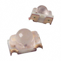
Surface Mount Type, High Power Output Infrared Emitting Diode
■ Features
1. 2. 3. 4. 5. 6. 7. Compact and thin SMD package Top view and side view mountable Plastic mold with resin lens Peak emission wavelength: 940 nm TYP. Narrow directivity angle (Δθ ±10° TYP.) High power output (φ e: 6.0 mW MAX.) Lead free and RoHS directive compliant
■ Agency Approvals/Compliance
1. Compliant with RoHS directive (2002/95/EC) 2. Content information about the six substances specified in “Management Methods for Control of Pollution Caused by Electronic Information Products Regulation” (popular name: China RoHS) (Chinese: ); refer to page 7.
■ Model Line-up
Model No. GL100MN1MP GL100MN1MP1 Packaging 2000 pcs/reel 1500 pcs/reel Mount Direction Side view Top view
■ Applications
1. 2. 3. 4. 5. 6. 7. Office automation equipment Audio visual equipment Home appliances Telecommunication equipment Measuring equipment Tooling machines Computers
Notice The content of data sheet is subject to change without prior notice. In the absence of confirmation by device specification sheets, SHARP takes no responsibility for any defects that may occur in equipment using any SHARP devices shown in catalogs, data books, etc. Contact SHARP in order to obtain the latest device specification sheets before using any SHARP device.
1
Sheet No.: D1-A00701EN Date: November 30, 2007 ©SHARP Corporation
�GL100MN1MPx ■ External Dimensions
3.0
2.2
(0.35) 0.75 0.65
0.95
(0.2)
1.5 R0.8
2.2 1.0
(0.57)
(0.65)
(0.57)
Pin Arrangement 1 No. 1 Name Anode Cathode
1
2
0.4
(0.4)
2
2
(1.0)
(1.0) Viewed from PCB (Top view Mounting) 3.0
Viewed from PCB (Side view Mounting) 3.0 1.5
0.85
1.5
1.1
1.4
NOTES: 1. Unit: mm 2. Unspecified tolerance : ±0.2 mm 3. ( ) : Reference dimensions 4. Au-plated area 5. Do not allow circuit runs in area
1.1
1.1
1.1
(Lens center)
1.7
1.5
Sheet No.: D1-A00701EN
2
�GL100MN1MPx ■ Absolute Maximum Ratings
Parameter Forward current Peak pulsed forward current *1 Reverse voltage Power dissipation Operating temperature Storage temperature Soldering temperature *2
100 µs, Duty ratio: 0.01 *1 Pulse width: see reflow profile on page 6. *2 10 s (MAX.)
(Ta = 25°C)
Symbol IF IFM VR P Topr Tstg Tsol
Rating 50 0.5 6 75 -30 to +85 -40 to +95 240
Unit mA A V mW °C °C °C
■ Electro-optical Charactertistics
Parameter Forward voltage Peak forward voltage Reverse current Radiant flux Peak emission wavelength Half intensity wavelength Terminal capacitance Response frequency Half intensity angle Symbol VF VFM IR φe λp Δλ Ct fC Δθ Conditions IF = 20 mA IFM = 0.5 A VR = 3 V IF = 20 mA IF = 5 mA IF = 5 mA VR = 0, f = 1 MHz – – MIN. – – – 2.0 – – – – – TYP. 1.2 3.0 – – 940 45 50 300 ±10 MAX. 1.5 4.0 10 6.0 – – – – –
(Ta = 25°C)
Unit V V µA mW nm nm pF kHz degrees
Fig. 1 Forward Current vs. Ambient Temperature
60 50 Forward current IF (mA) 40 30 20 10
Fig. 2 Peak Forward Current vs. Duty Ratio
10000 Peak forward current IFM (mA) Pulse width ≤ 100 µs Ta = 25°C
1000
100
10 10-4
10-3
10-2 Duty ratio
10-1
100
0 -50
-30 -25
85 0 25 50 75 100 Ambient temperature Ta (°C)
Sheet No.: D1-A00701EN
3
�GL100MN1MPx
Fig. 3 Spectral Distribution
100 IF = 5 mA Ta = 25°C Relative radiant intensity (%) 80
Fig. 5 Forward Current vs. Forward Voltage
1,000
Ta = 85°C Forward current IF (mA) 100
60
50°C 10 25°C 0°C -30°C 1
40
20
0 860 880 900 920 940 960 980 1000 1020 1040 Wavelength λ (nm)
0.1 0 0.5 1 1.5 2 2.5 3
Forward voltage VF (V)
Fig. 4 Peak Emission Wavelength vs. Ambient Temperature
980 IF = constant Peak emission wavelength λp (nm) 970
Fig. 6 Relative Radiant Flux vs. Ambient Temperature
10 IF = constant
960
950
Relative radiant flux (%) 0 25 50 75 85 100
1
940
930
920 -50 -30 -25
0.1 -50
-30 -25
0
25
50
75 85 100
Ambient temperature Ta (°C)
Ambient temperature Ta (°C)
Sheet No.: D1-A00701EN
4
�GL100MN1MPx
Fig. 7 Radiant Flux vs. Forward Current
100 Ta = 25°C
Fig. 9 Radiation Diagram (Typical Value)
-20° -10° 0° 100 -30° 80 Relative radiant intensity (%) +10° +20° Ta = 25°C +30°
Radiant flux Φe (mW)
10 -40° Pulse (Pulse width ≤ 100 μs) -50° 1 -60° -70° -80° 0.1 1 10 100 1000 -90°
60
+40°
40
+50° +60°
20 +70° +80° 0 +90°
Forward current IF (mA)
Angular displacement θ
Fig. 8 Relative Output vs. Distance to Detector
(Detector: PT100MF0MP) 100 IF = constant Ta = 25°C
10 Relative output (%)
1
0.1
0.01 0.1
1
10
100
1000
Distance to detector d (mm)
Sheet No.: D1-A00701EN
5
�GL100MN1MPx ■ Design Considerations
Design Guidelines 1. Allow for natural degradation of the LED as a result of long continuous operation. This part will have 50% degradation in output after 5 years of continuous use. 2. This product is not designed to be electromagnetic- and ionized-particle-radiation resistant.
■ Manufacturing Guidelines
Soldering Instructions 1. Sharp recommends soldering no more than once when using solder reflow methods. 2. When using solder reflow methods, follow the reflow soldering temperature profile shown in Fig. 10. Sharp recommends checking the process to make sure these parameters are not exceeded; exceeding these parameters can cause substrate bending or other mechanical stresses leading to debonding of the internal gold wires, or other similar failure modes. 3. If using an infrared lamp to preheat the parts, such heat sources may cause localized high temperatures in the part's resin. Be sure to keep the temperature profile within the guidelines shown in Fig. 10. 4. If hand soldering, use temperatures ≤ 260° for ≤ 3 seconds. Do not dip-solder or VPS-solder this part. 5. Do not subject the package to excessive mechanical force during soldering as it may cause deformation or defects in plated connections. Internal connections may be severed due to mechanical force placed on the package due to the PCB flexing during the soldering process.
Fig. 10 Reflow Soldering Temperature Profile
240°C MAX. 200°C 1 ~ 4°C/s 165°C MAX. 1 ~ 4°C/s 1 ~ 4°C/s
25°C 10s MAX. 60s MAX. 120s MAX. 90s MAX.
Cleaning Instructions 1. Confirm this device's resistance to process chemicals before use, as certain process chemicals may affect the optical characteristics. 2. Solvent cleaning: Solvent temperature should be 45°C or below. Immersion time should be 3 minutes or less. 3. Ultrasonic cleaning: The effect upon devices varies due to cleaning bath size, ultrasonic power output, cleaning time, PCB size and device mounting circumstances. Sharp recommends testing using actual production conditions to confirm the harmlessness of the ultrasonic cleaning methods. 4. Recommended solvent materials: Ethyl alcohol, Methyl alcohol, and Isopropyl alcohol.
Sheet No.: D1-A00701EN
6
�GL100MN1MPx
Storage and Handling 1. Store these parts between 5°C and 30°C, at a relative humidity of less than 70%. 2. After breaking the package seal, maintain the environment within 5°C to 25°C, at a relative humidity of less than 60%, and mount the parts within two days. If unable to do so, bake before mounting. 3. When storing the parts after breaking the seal, Sharp recommends storage of no longer than two weeks in a dry box or by resealing the parts in a moisture-proof bag with a desiccant. If unable to do so, bake before mounting. 4. When baking the parts before mounting, Sharp recommends baking the parts only once and only if in a metal tray or mounted on a PCB. Recommended conditions are for 16 to 24 hours, at a temperature of 125°C.
■ Presence of ODCs (RoHS Compliance)
This product shall not contain the following materials, and they are not used in the production process for this product: • Regulated substances: CFCs, Halon, Carbon tetrachloride, 1,1,1-Trichloroethane (Methylchloroform). Specific brominated flame retardants such as the PBBOs and PBBs are not used in this product at all. This product shall not contain the following materials banned in the RoHS Directive (2002/95/EC). • Lead, Mercury, Cadmium, Hexavalent chromium, Polybrominated biphenyls (PBB), Polybrominated diphenyl ethers (PBDE). • Content information about the six substances specified in “Management Methods for Control of Pollution Caused by Electronic Information Products Regulation” (Chinese: )
Toxic and Hazdardous Substances Category Lead (Pb) mercury (Hg) Cadmium (Cd) ✓ ✓ ✓ Hexavalent chromiun (Cr6+) ✓ Polybrominated biphenyls (PBB) ✓ Polybrominated diphenyl ethers (PBDE) ✓
Infrared Emitting Diode
NOTE: ✓ indicates that the content of the toxic and hazardous substance in all the homogeneous materials of the part is below the concentration limit requirement as described in SJ/T 11363-2006 standard.
■ Taping Specifications
1. 2. 3. 4. 5. 6. Tape structure and dimensions conforms to those shown in Fig. 11 to Fig. 16. Product insertion will have the cathode to the hole side of the tape. Cover tape peel-separation force: F = 0.2 to 1.0 N (where θ 160° to 180°) Quantity per reel = 2000 pcs. (GL100MN1MP) or 1500 pcs. (GL100MN1MP1) Product mass: 0.01 g (approx.) Packaging: a. Reels are sealed inside an aluminum bag, along with a humidity indicator card. b. Bags are labeled and securely packed.
Sheet No.: D1-A00701EN
7
�GL100MN1MPx ■ Packing Specifications ● GL100MN1MP (Side view mount, 2000 pcs/reel) Fig. 11 Tape Shape and Dimension
4.0 ±0.1 2.0 ±0.05 φ1.5 +0.1 -0 1.75 ±0.1 0.3 ±0.05 1.75 ±0.1
3.5 ±0.05 1.7 ±0.1 5.5 ±0.1 3.3 ±0.1
8.0 ±0.3
4.0 ±0.1 1.6 ±0.1 2.5 ±0.1
Fig. 12 Reel Shape and Dimension
9.0 -0 2.0 ±0.5 φ13.0 ±0.2
+0.3
180.0 NOTE: Unit: mm
60.0 -0
+1
11.4 ±1
5°
Sheet No.: D1-A00701EN
8
�GL100MN1MPx
Fig. 13 Product Insertion Direction
Pull-out direction
● GL100MN1MP1 (Top view mount, 1500 pcs/reel) Fig. 14 Tape Shape and Dimension
4.0 ±0.1 2.0 ±0.05 φ1.5 +0.1 -0 1.75 ±0.1 0.3 ±0.05 2.45 ±0.1
3.5 ±0.05 5.5 ±0.1 3.3 ±0.1
8.0 ±0.3
4.0 ±0.1 1.8 ±0.1
5°
Sheet No.: D1-A00701EN
9
�GL100MN1MPx
Fig. 15 Reel Shape and Dimension
9.0 -0 2.0 ±0.5 φ13.0 ±0.2
+0.3
180.0
60.0 -0
+1
11.4 ±1
NOTE: Unit: mm
Fig. 16 Product Insertion Direction
Pull-out direction
Sheet No.: D1-A00701EN
10
�GL100MN1MPx ■ Important Notices
· The circuit application examples in this publication are provided to explain representative applications of SHARP devices and are not intended to guarantee any circuit design or license any intellectual property rights. SHARP takes no responsibility for any problems related to any intellectual property right of a third party resulting from the use of SHARP’s devices. · Contact SHARP in order to obtain the latest device specification sheets before using any SHARP device. SHARP reserves the right to make changes in the specifications, characteristics, data materials, structure, and other contents described herein at any time without notice in order to improve design or reliability. Manufacturing locations are also subject to change without notice. · Observe the following points when using any devices in this publication. SHARP takes no responsibility for damage caused by improper use of the devices which does not meet the conditions and absolute maximum ratings to be used specified in the relevant specification sheet nor meet the following conditions: (i) The devices in this publication are designed for use in general electronic equipment designs such as: --- Personal computers --- Office automation equipment --- Telecommunication equipment (terminal) --- Test and measurement equipment --- Industrial control --- Audio visual equipment --- Consumer electronics (ii) Measures such as fail-safe function and redundant design should be taken to ensure reliability and safety when SHARP devices are used for or in connection with equipment that requires higher reliabilty such as:
--- Transportation control and safety equipment (i.e., aircraft, trains, automobiles, etc.) --- Traffic signals --- Gas leakage sensor breakers --- Alarm equipment --- Various safety devices, etc. (iii) SHARP devices shall not be used for or in connection with equipment that requires an extremely high level of reliability and safety such as: --- Space applications --- Telecommunication equipment (trunk lines) --- Nuclear power control equipment --- Medical and other life support equipment (e.g. scuba) · If the SHARP devices listed in this publication fall within the scope of strategic products described in the Foreign Exchange and Foreign Trade Law of Japan, it is necessary to obtain approval to export such SHARP devices. · This publication is the proprietary product of SHARP and is copyrighted, with all rights reserved. Under the copyright laws, no part of this publication may be reproduced or transmitted in any form or by any means, electronic or mechanical, for any purpose, in whole or in part, without the express written permission of SHARP. Express written permission is also required before any use of this publication may be made by a third party. · Contact and consult with a SHARP representative if there are any questions about the contents of this publication.
Sheet No.: D1-A00701EN
11
�