GP1A91LRJ00F
GP1A91LRJ00F
Gap : 1.2mm, Slit : 0.23mm *OPIC Output, Compact Transmissive Photointerrupter
■ Description
GP1A91LRJ00F is a compact-package, OPIC output, transmissive photointerrupter, with opposing emitter and detector in a molding that provides non-contact sensing. The compact package series is a result of unique technology combing transfer and injection molding. This device has 2 positioning bosses on the detector side, and pull-up resistor included in the deviceʼs output.
■ Agency approvals/Compliance
1. Compliant with RoHS directive
■ Applications
1. Detection of object presence or motion. 2. Example : printer, lens control for camera
■ Features
1. Transmissive with OPIC output 2. Highlights: • Compact Size 3. Key Parameters: • Gap Width : 1.2mm • Slit Width (detector side): 0.23mm • Package : 3.7×2.6×3.1mm 4. Lead free and RoHS directive compliant
* "OPIC"(Optical IC) is a trademark of the SHARP Corporation. An OPIC consists of a light-detecting element and a signalprocessing
Notice The content of data sheet is subject to change without prior notice. In the absence of confirmation by device specification sheets, SHARP takes no responsibility for any defects that may occur in equipment using any SHARP devices shown in catalogs, data books, etc. Contact SHARP in order to obtain the latest device specification sheets before using any SHARP device.
1
Sheet No.: D3-A01501EN Date Oct. 3. 2005 © SHARP Corporation
�GP1A91LRJ00F
■ Internal Connection Diagram
Top view (15kΩ)
3 4 1 1 2 3 4 2 5
5
Amp.
Anode Cathode VCC VO GND
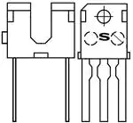
■ Outline Dimensions
Top view b' a'
(Unit : mm)
1.4 0.3 b a 3.7 1.2 (C0.4) Emitter Center (C0.3) 0.15+0.2 −0.1 ∗2.65 SHARP mark "S"
5 1
1.25 (0.85)
a-a' section 2.6 2 (0.8)
2.3
3.1
φ0.6 3.6±0.5 Residual gates 0.4 ∗1 ∗1 b-b' section (0.23)
4 3 2
• Unspecified tolerance : ±0.2mm. • ( ) : Reference dimensions. • The dimensions indicated by ∗ refer to those measured from the lead base. • The dimensions shown do not include burr. Burr's dimension : 0.15mm MAX. Rest of gate : 0.3mm MAX.
Product mass : approx. 0.052g Plating material : SnCu (Cu : TYP. 2%)
Country of origin
Japan
Sheet No.: D3-A01501EN
2
�GP1A91LRJ00F
■ Absolute Maximum Ratings
Parameter ∗1 Forward current Reverse voltage Input Power dissipation Supply voltage Output ∗1Low level output current ∗1 Power dissipation Operating temperature Storage temperature ∗2 Soldering temperature
∗ ∗
Symbol Rating IF 50 VR 6 P 75 VCC 7 IO 2 PO 80 Topr −25 to +85 Tstg −40 to +100 Tsol 260
(Ta=25˚C) Unit mA V mW V mA mW ˚C ˚C ˚C
1mmMIN. Soldering area
1 Refer to Fig.2, 3, 4 2 For 5s or less
■ Electro-optical Characteristics
Parameter Forward voltage Input Reverse current Operating supply voltage Low level output voltage High level output voltage Output Low level supply current High level supply current ∗3 "High→Low" threshold input current ∗4 Hysteresis Transfer "Low→High" Propagation delay time charac"High→Low" Propagation delay time teristics Rise time Fall time Response time
∗ ∗
Symbol VF IR VCC VOL VOH ICCL ICCH IFHL IFLH/IFHL tPLH tPHL tr tf
Condition IF=5mA VR=3V − VCC=3V, IOL=1mA, IF=5mA VCC=3V, IF=0 VCC=3V, IF=5mA VCC=3V, IF=0 VCC=3V VCC=3V VCE=3V, IF=5mA, RL=3kΩ
MIN. − − 1.4 − 2.9 − − − 0.55 − − − −
TYP. 1.15 − − 0.1 − 0.7 0.3 1.2 0.8 10 3 0.6 0.2
(Ta=25˚C) MAX. Unit 1.25 V 10 μA 7 V 0.4 V V − 1.2 mA 0.5 mA 3.5 mA 0.95 − 30 15 μs 3 1
3 IFHL represents forward current when output goes from "High" to "Low". 4 Hysteresis stands for IFLH/IFHL. IFLH represents forward current when output goes from "High" to "Low".
Sheet No.: D3-A01501EN
3
�GP1A91LRJ00F
Fig.1 Test Circuit for Response Time
VCC 3V Amp. Vin 47Ω 0.1μF GND tr=tf=0.01μs ZO=50Ω tf tr (15kΩ) 3kΩ VO tPHL tPLH V 90% OH 1.5V 10% V
OL
Input
50%
Fig.2 Forward Current vs. Ambient Temperature
60 50 Forward current IF (mA) 40 30 20 10 0 −25
Fig.3 Output Current vs. Ambient Temperature
3 2.5 Output current IO (mA) 2 1.5 1 0.5 0.4
0
25
50
75 85
100
0 −25
0
25
50
75 85
100
Ambient temperature Ta (˚C)
Ambient temperature Ta (˚C)
Fig.4 Output Power Dissipation vs. Ambient Temperature
120 100 80 60 40 20 16 0 −25
Fig.5 Forward Current vs. Forward Voltage
Ta =75˚C 50˚C Forward current IF (mA) 100
Output power dissipation PO (mW)
25˚C 0˚C −25˚C
10
1 0 25 50 75 85 100 0 0.5 1 1.5 2 2.5 3 3.5 Ambient temperature Ta (˚C) Forward voltage VF (V)
Sheet No.: D3-A01501EN
4
�GP1A91LRJ00F
Fig.6 Relative Input Threshold Current vs. Supply Voltage
1.2 Relative threshold input current IFHL,IFLH IFHL 1 0.8 0.6 0.4 0.2 0 0 2.5 5 7.5 10 Supply voltage VCC (V) Ta = 25˚C IFHL = 1 at VCC = 3V
Fig.7 Relative Input Threshold Current vs. Ambient Temperature
1.6 Relative threshold input current IFHL,IFLH 1.4 1.2 1 IFLH 0.8 0.6 0.4 0.2 −25 VCC=3V IFHL=1 at Ta=25˚C IFHL
IFLH
0
25
50
75
100
Ambient temperature Ta (˚C)
Fig.8 Low Level, High Level Supply Current vs. Supply Voltage (1)
2.2 Low level, high level supply current ICC (mA) 2 1.8 1.6 1.4 1.2 1 0.8 0.6 0.4 0.2 0 0 1 2 3 4 5 6 7 8 9 10 Supply voltage VCC (V) ICCH ICCL ICCL:IF=5mA ICCH:IF=0mA Ta=−25˚C
Fig.9 Low Level, High Level Supply Current vs. Supply Voltage (2)
2.2 Low level, high level supply current ICC (mA) 2 1.8 1.6 1.4 1.2 1 0.8 0.6 0.4 0.2 0 0 1 2 3 4 5 6 7 8 9 10 Supply voltage VCC (V) ICCH ICCL ICCL:IF=5mA ICCH:IF=0mA Ta=25˚C
Fig.10 Low Level, High Level Supply Current vs. Supply Voltage (3)
2.2 Low level, high level supply current ICC (mA) 2 1.8 1.6 1.4 1.2 1 0.8 0.6 0.4 0.2 0 0 1 2 3 4 5 6 7 8 9 10 Supply voltage VCC (V) ICCH ICCL ICCL:IF=5mA ICCH:IF=0mA Ta=85˚C
Fig.11 Low Level Output Voltage vs. Low Level Output Current
220 200 Low level output voltage VOL (mV) 180 160 140 120 100 80 60 40 20 0 0 0.3 0.6 0.9 1.2 1.5 1.8 2.1 2.4 2.7 Low level output current IOL (mA)
Sheet No.: D3-A01501EN
IF=5mA VCC=3V Ta=25˚C
3
5
�GP1A91LRJ00F
Fig.12 Low Level Output Voltage vs. Ambient Temperature
0.4 IF=5mA VCC=3V 0.3
Fig.13 Rise Time, Fall Time vs. Load Resistance
0.6 0.5 Rise time, fall time tf,tr (μs) 0.4 0.3 0.2 0.1 0 0.1 VCC=3V IF=5mA Ta=25˚C tr
Low level output voltage VOL (V)
0.2
IOL=2mA IOL=1mA
0.1 IOL=0mA 0 −25
tf
0
25
50
75
100
1
10
100
Ambient temperature Ta (˚C)
Load resistance RL (kΩ)
Fig.14 Propagation Delay Time vs. Forward Current
10 Propagation delay time tPHL,tPLH (μs) VCC=3V RL=3kΩ Ta=25˚C tPLH
Fig.15 Low, High Level Output vs. Shield Distance (1) (Typical Value)
IF=5mA VCC=3V Ta=25˚C High Low, high level output
L=0 Shield Sensor
8
6
Shield distance L
4
2
tPHL
Low
0 0 10 20 30 40 50 Forward current IF (mA)
−1
0
1
2
3
Shield moving distance L (mm)
Fig.16 Low, High Level Output vs. Shield Distance (1) (Typical Value)
IF=5mA VCC=3V Ta=25˚C High Low, high level output
Shield distance L Shield L=0 Sensor
Low
−1
0
1
2
Shield moving distance L (mm)
Remarks : Please be aware that all data in the graph are just for reference and not for guarantee.
Sheet No.: D3-A01501EN
6
�GP1A91LRJ00F
■ Design Considerations ● Recommended operating conditions
Parameter Output current Forward current Operating Supply voltage Operating temperature Symbol IO IF VCC Topr MIN. − 7 1.6 0 MAX. 1 10 7 70 Unit mA mA V ˚C
● Notes about static electricity
Transisiter of detector side in bipolar configuration may be damaged by static electricity due to its minute design. When handing these devices, general countermeasure against static electricity should be taken to avoid breakdown of devices or degradation of characteristics.
● Design guide
In order to stabilize power supply line, we should certainly recommend to connect a by-pass capacitor of 0.01µF or more between VCC and GND near the divice. 1) Prevention of detection error To prevent photointerrupter from faulty operation caused by external light, do not set the detecting face to the external light. 2) Position of opaque board Opaque board shall be installed at place 1.6mm or more from the top of elements. (Example)
1.6mm or more
1.6mm or more
This product is not designed against irradiation and incorporates non-coherent IRED.
● Degradation
In general, the emission of the IRED used in photointerrupter will degrade over time. In the case of long term operation, please take the general IRED degradation (50% degradation over 5 years) into the design consideration. Please decide the input current which become 2 times of MAX. IFHL.
Sheet No.: D3-A01501EN
7
�GP1A91LRJ00F
● Parts
This product is assembled using the below parts.
• Photodetector (qty. : 1) [Using a silicon photodiode as light detecting portion, and a bipolar IC as signal processing circuit]
Category Photo diode Material Silicon (Si) Maximum Sensitivity wavelength (nm) 900 Sensitivity wavelength (nm) 700 to 1 200 Response time (μs) 3
• Photo emitter (qty. : 1)
Category Infrared emitting diode (non-coherent) Material Gallium arsenide (GaAs) Maximum light emitting wavelength (nm) 950 I/O Frequency (MHz) 0.3
• Material
Case Black polyphernylene sulfide resin (UL94 V-0) Lead frame 42Alloy Lead frame plating SnCu plating
• Others
Laser generator is not used.
Sheet No.: D3-A01501EN
8
�GP1A91LRJ00F
■ Manufacturing Guidelines ● Soldering Method Flow Soldering:
Soldering should be completed below 260˚C and within 5 s. Please solder within one time. Soldering area is 1mm or more away from the bottom of housing. Please take care not to let any external force exert on lead pins. Please don't do soldering with preheating, and please don't do soldering by reflow.
Hand soldering
Hand soldering should be completed within 3 s when the point of solder iron is below 350̊C. Please solder within one time. Please don't touch the terminals directly by soldering iron. Soldered product shall treat at normal temperature.
Other notice
Please test the soldering method in actual condition and make sure the soldering works fine, since the impact on the junction between the device and PCB varies depending on the cooling and soldering conditions.
● Cleaning instructions Solvent cleaning :
Solvent temperature should be 45˚C or below. Immersion time should be 3 minutes or less.
Ultrasonic cleaning :
Do not execute ultrasonic cleaning.
Recommended solvent materials :
Ethyl alcohol, Methyl alcohol and Isopropyl alcohol.
● Presence of ODC
This product shall not contain the following materials. And they are not used in the production process for this product. Regulation substances : CFCs, Halon, Carbon tetrachloride, 1.1.1-Trichloroethane (Methylchloroform) Specific brominated flame retardants such as the PBBOs and PBBs are not used in this product at all. This product shall not contain the following materials banned in the RoHS Directive (2002/95/EC). •Lead, Mercury, Cadmium, Hexavalent chromium, Polybrominated biphenyls (PBB), Polybrominated diphenyl ethers (PBDE).
Sheet No.: D3-A01501EN
9
�GP1A91LRJ00F
■ Package specification ● Sleeve package Package materials
Sleeve : Polystyrene Stopper : Styrene-Elastomer
Package method
MAX. 100 pcs. of products shall be packaged in a sleeve. Both ends shall be closed by tabbed and tabless stoppers. MAX. 50 sleeves in one case.
Sheet No.: D3-A01501EN
10
�GP1A91LRJ00F
■ Important Notices
· The circuit application examples in this publication are provided to explain representative applications of SHARP devices and are not intended to guarantee any circuit design or license any intellectual property rights. SHARP takes no responsibility for any problems related to any intellectual property right of a third party resulting from the use of SHARP's devices. · Contact SHARP in order to obtain the latest device specification sheets before using any SHARP device. SHARP reserves the right to make changes in the specifications, characteristics, data, materials, structure, and other contents described herein at any time without notice in order to improve design or reliability. Manufacturing locations are also subject to change without notice. · Observe the following points when using any devices in this publication. SHARP takes no responsibility for damage caused by improper use of the devices which does not meet the conditions and absolute maximum ratings to be used specified in the relevant specification sheet nor meet the following conditions: (i) The devices in this publication are designed for use in general electronic equipment designs such as: --- Personal computers --- Office automation equipment --- Telecommunication equipment [terminal] --- Test and measurement equipment --- Industrial control --- Audio visual equipment --- Consumer electronics (ii) Measures such as fail-safe function and redundant design should be taken to ensure reliability and safety when SHARP devices are used for or in connection with equipment that requires higher reliability such as: --- Transportation control and safety equipment (i.e., aircraft, trains, automobiles, etc.) --- Traffic signals --- Gas leakage sensor breakers --- Alarm equipment --- Various safety devices, etc. (iii) SHARP devices shall not be used for or in connection with equipment that requires an extremely high level of reliability and safety such as: --- Space applications --- Telecommunication equipment [trunk lines] --- Nuclear power control equipment --- Medical and other life support equipment (e.g., scuba). · If the SHARP devices listed in this publication fall within the scope of strategic products described in the Foreign Exchange and Foreign Trade Law of Japan, it is necessary to obtain approval to export such SHARP devices. · This publication is the proprietary product of SHARP and is copyrighted, with all rights reserved. Under the copyright laws, no part of this publication may be reproduced or transmitted in any form or by any means, electronic or mechanical, for any purpose, in whole or in part, without the express written permission of SHARP. Express written permission is also required before any use of this publication may be made by a third party. · Contact and consult with a SHARP representative if there are any questions about the contents of this publication.
[H140]
Sheet No.: D3-A01501EN
11
�