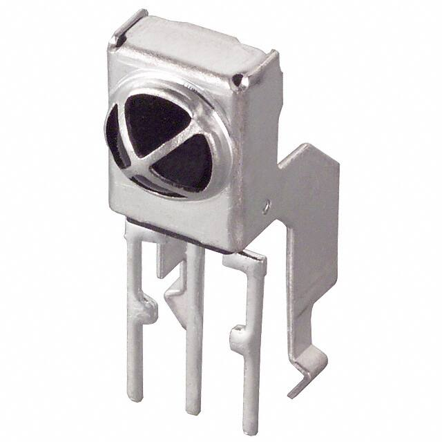
GP1UM26RK/27RK/28RK/28QK Series
GP1UM26RK/GP1UM27RK Series
GP1UM28RK/GP1UM28QK Series
Anti Electromagnetic Induction
Noise Type Compact IR Detecting
Unit for Remote Control
■ Features
■ Applications
1. Anti electromagnetic induction noise type.
2. Compact (case volume).
3. Various B.P.F. (Band Pass Frequency) frequency to meet different
user needs.
1. AV equipments
2. Home appliances
■ Outline Dimensions
(Unit : mm)
GP1UM26RK Series
GP1UM27RK Series
*1
9.6
3.6±0.5
*3
Center
of PD
9.6
7.6
*2
2.54
3.6±0.5
13.8±0.5
1.4
2
1
2.54
0.8
Example of mounting drawing
from solder side (Reference)
0.8
*3
0.5
1
1.*1 : Indicates root dimensions of connector.
2.Unspecified tolerance : ±0.3
3.Case thickness : 0.3TYP
4.*2 : Exclude sagged solder
5.*3 : If there are difficulties to insert the GP1UM26RK series on PCB,
we recommend to expand +0.1mm from original 2.9mm.
*3
0.8
2
*1
2.54
*1
2.54
3
1 VOUT
2 VCC
3 GND
5.8
*3
2.9
2.9
1.4
1.4
Center
of PD
3
2.54
2
1
3−
φ
1.7
3
2.54
3−
φ
5.85
7.55
6.7
2.9
1.4
*1
*1
5.8
2.9
3.6
0.4
*3
1.7
2.54
*3
1 VOUT
2 VCC
3 GND
7.55
6.7
*1
3
4.3 2.9
4.7
2
1.7
1
0.5
Example of mounting drawing
from solder side (Reference)
5.85
0.7
1.7
0.7
10.2
2.2
5.6
0.5
1.4
2.2
±0.5
1.4
8.6
1.25
*1
0.4
1.4
7.6
4.3 2.9
4.7
3.6
0.5
1.4
2.2
1.25
5
2.2
5.6
0.8
2.54
1.*1 : Indicates root dimensions of connector.
2.Unspecified tolerance : ±0.3
3.Case thickness : 0.3TYP
4.*2 : Exclude sagged solder
5.*3 : If there are difficulties to insert the GP1UM27RK series on PCB,
we recommend to expand +0.1mm from original 2.9mm.
Notice
In the absence of confirmation by device specification sheets, SHARP takes no responsibility for any defects that may occur in equipment using any SHARP
devices shown in catalogs, data books, etc. Contact SHARP in order to obtain the latest device specification sheets before using any SHARP device.
Internet Internet address for Electronic Components Group http://sharp-world.com/ecg/
�GP1UM26RK/27RK/28RK/28QK Series
■ Outline Dimensions
(Unit : mm)
2.75
2.2
2.9
5.6
*2
9.6
1.25
4.3
1.25
GP1UM28QK Series
9.6
GP1UM28RK Series
0.8
0.5
1
2
9.6
Example of mounting drawing
from solder side (Reference)
2.54
2.54
3
8
*3
*3
2.9
2.9
1.4
1.4
1.4
*3
2.9
Top of lenz
3
2.9
*3
5.8
1.7
2
5.8
*1
2.54
1 VOUT
2 VCC
3 GND
1.4
Center
of PD
3
2.54
2
1
3−
φ
5.85
1
7.55
6.7
0.5
*1
1.7
*3
1.7
Example of mounting drawing
from solder side (Reference)
*3
2
3.55
3−φ
0.
0.8
2.54
1
3.9
1.25
1.25
17.8±0.5
0.8
1.4
1.85
3.6±0.5
1.4
5.4
6.8
1.7
*2
1.7
3.7
1 VOUT
2 VCC
3 GND
*1
0.4
1.4
7.6
4.3 2.9
4.7
3.6
2.54
2.54
0.5
1.4
2.2
14.2
2.2
0.8
*1
*1
5.6
3
3.6
0.4
*1
0.8
1.*1 : Indicates root dimensions of connector.
2.Unspecified tolerance : ±0.3
3.Case thickness : 0.3TYP
4.*2 : Exclude sagged solder
5.*3 : If there are difficulties to insert the GP1UM28QK series on PCB,
we recommend to expand +0.1mm from original 2.9mm.
2.54
1.*1 : Indicates root dimensions of connector.
2.Unspecified tolerance : ±0.3
3.Case thickness : 0.3TYP
4.*2 : Exclude sagged solder
5.*3 : If there are difficulties to insert the GP1UM28RK series on PCB,
we recommend to expand +0.1mm from original 2.9mm.
■ Model Line-up
Diversified models with a different B.P.F. frequency are also available.
Model No.
B.P.F. center frequency
40
GP1UM26RK
GP1UM27RK
GP1UM28RK
36
GP1UM260RK
GP1UM270RK
GP1UM280RK
38
GP1UM261RK
GP1UM271RK
GP1UM281RK
36.7
GP1UM262RK
GP1UM272RK
GP1UM282RK
56.8
GP1UM267RK
GP1UM277RK
GP1UM287RK
Unit
GP1UM28QK
GP1UM280QK
GP1UM281QK
GP1UM282QK
GP1UM287QK
kHz
�GP1UM26RK/27RK/28RK/28QK Series
■ Internal Block Diagram
RL
VOUT
Limiter
B.P.F. Demodulator Integrator Comparator
VCC
GND
■ Absolute Maximum Ratings
Parameter
Supply voltage
*1
Operating temperature
Storage temperature
*2
Soldering temperature
Symbol
VCC
Topr
Tstg
Tsol
(Ta=25°C)
Rating
Unit
V
0 to +6.0
−10 to +70
°C
−20 to +70
°C
260
°C
■ Recommended Operating Conditions
Parameter
Supply voltage
Symbol Operating conditions
VCC
4.5 to 5.5
Unit
V
*1 No dew condensation is allowed
*2 For 5s (At mounting on PCB with thickness of 1.6mm)
■ Electro-optical Characteristics
Parameter
Dissipation current
High level output voltage
Low level output voltage
High level pulse width
Low level pulse width
B.P.F. center frequency
Output pull-up resistance
Symbol
Conditions
ICC
VOH
VOL
T1
T2
f0
RL
No input light
*3
IOL=1.6mA
−
−
(Ta=25˚C, VCC=+5V)
MIN. TYP. MAX. Unit
0.95
1.5
−
mA
−
−
V
VCC −0.5
−
−
V
0.45
µs
−
1 200
600
µs
−
400
1 000
*4
−
−
kHz
70
100
130
kΩ
*3 The burst wave as shown in the following figure shall be transmitted by the transmitter shown in Fig. 1
The carrier frequency of the transmitter, however, shall be same as *4, and measurement shall be from just after starting the transmission until 50 pulse
*4 The B.P.F. center frequency f0 varies with model, as shown in ■ Model Line-up
Burst wave
600µs
1 000µs
f0=(*4)
Duty 50%
�GP1UM26RK/27RK/28RK/28QK Series
■ Performance
Using the transmitter shown in Fig. 1, the output signal of the light detecting unit is good enough to meet the following items in the
standard optical system in Fig. 2.
1. Linear reception distance characteristics
When L=0.2 to 8.5(7.0)*7m, *5EV
很抱歉,暂时无法提供与“GP1UM281QK”相匹配的价格&库存,您可以联系我们找货
免费人工找货