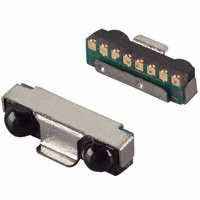
GP2W0110YPS/GP2W0114YPS
IrDA Technical Information
Low Power Infrared Transceiver
DESCRIPTION
The SHARP GP2W0110YPS/GP2W0114YPS are low-power, short-range infrared transceiver modules. They meet the Mobile Communication Low Power Option within the IrDA Specification for the 20 cm communication range. When operating at lower supply voltages, these units provide a reliable interface between logic and IR signals. Applications include through-air, serial, half-duplex IR wireless data links at rates up to 115 kbit/s and the devices are designed to satisfy the IrDA Physical Layer Specifications. The SHARP GP2W0110YPS/GP2W0114YPS infrared transceiver modules contain a high speed, high efficiency, low power consumption AlGaAs LED, silicon PIN photodiode, and the low power driven bipolar integrated circuit. The IC contains a LED driver circuit and a receiver that provides the Rx output supporting 2.4 kbit/s to 115.2 kbit/s IrDA signals. They meet the IrDA Low Power Option Communication Standard link distance of 0.2 m with low power devices and 0.3 m with standard devices. The GP2W0110YPS/GP2W0114YPS include a constant-current source in the LED driver circuit that eliminates the need for an external current limiting resistor in the LED circuit. The IrDA Low Power Option Standard is most suitable for telecommunication products and mobile terminals, such as cellular phones, paging devices, and PDA-cellular combined multimedia devices. The transceiver modules provide wireless data link capability for cellular phones and pagers, PDAs, or any other IrDA application already on the market. The transceiver modules’ receiver electronics operate at voltages from 2.0 V through 3.6 V without any performance degradation. The split-voltage supply allows the LED voltage to come from a separate supply. An example is in cell phones where the LED may operate from the battery and the receiver and logic section is supplied from a regulated supply at a lower voltage. This provides manufacturers with the advantage of an energy saving design in any application field, with alternatives for supply voltage and flexibility for other components. The GP2W0110YPS/GP2W0114YPS transceiver modules have a built-in 0.1 µA Shutdown mode for those applications that are very conscious about current consumption. Additionally, the GP2W0110YPS/GP2W0114YPS have a tri-state output, which allow their use in applications where one port connection may be connected to more than one device. The included shield is appropriate in applications where Electro-Magnetic Interference (EMI) is a concern. Infrared energy is immune to EMI, but the receiving PIN photodiode is somewhat sensitive to EMI. This is the case in all IR communication devices.
FEATURES
• IrDA Low Power Option Compatibility for Telecommunication and Mobile Terminals • Industry Low Volume Package Design for a Low Power Transceiver: – 7.6(W) × 2.65(D) × 2.0(H) mm, 40.28 mm3 • Low Power Consumption with Built-in Shut-Down Mode 0.2 µA (TYP.) • Low and Wide Range Operating Voltage: – VDD = 2.0 V to 3.6 V, VLEDA = 2.0 V to 6.0 V • Soldering Reflow Capable • SMD Lead-less Package Design Provides Flexibility with either Vertical Mount or Horizontal Mount to PCBs • Replaces GP2W0102YP, GP2W0104YP, and GP2W0106YP • Added Features include Tri-state Output and Splitvoltage Supply Capability • Fully Compatible with Agilent HSDL 3201 • TOP View Version: GP2W0114YPS
APPLICATIONS
• Telecommunication Products – Cellular Phones – Pagers – Smart Phones • Mobile Products – PDAs – Electronic Wallets – Mini-Notebook PCs • Imaging Products – Portable Printers – Portable Text Scanners
IrDA Technical Information
1
�GP2W0110YPS/GP2W0114YPS
Low Power Infrared Transceiver
OUTLINE DIMENSIONS
The dimensions below are only for design reference, and are subject to change without notice. The metal
shield case provides excellent noise immunity. Contact your local SHARP office for the latest device specifications.
5.7
2.85 ±0.3
2.5 7.9 ±0.3 5.2 2.0 ±0.3 1.05 ±0.3 0.8 - 0.2
+0.3
CENTER OF DETECTOR
CARVED SEAL
CENTER OF EMITTER
1
2
0.2 8 - 0.4 +0.3 -
3
4
5
6
7
8
PO. 95 × 7 = 6.65
PIN 1 2 3 4 5 6 7 8 NC NC VCC
PIN NAME
SYMBOL NC NC 0.6 ±0.3 8 - 0.6 PO. 95 × 7 = 6.65
GP2W0110YPS-15
VCC GND SD RxD TxD LEDA
Ground Shutdown Receiver Data Output Transmitter Data Input LED Anode
NOTES: 1. Dimensions are in mm. 2. Unspecified tolerances are ±0.2 3. Adhesion of resin to the terminal area are allowed 0.2 mm MAX. 4. area: Gold plating
Figure 1. GP2W0110YPS/GP2W0114YPS Outline Dimensions
2
0.35
2.15 ±0.3
φ2.2
φ2.0
1.5 ±0.3
2.75 ±0.3
IrDA Technical Information
�Low Power Infrared Transceiver
GP2W0110YPS/GP2W0114YPS
ABSOLUTE MAXIMUM RATINGS
PARAMETER Supply Voltage LED Supply Voltage Peak Forward LED Current Operating Temperature Storage Temperature Soldering Temperature* SYMBOL MIN. MAX. UNIT VDD VLEDA IFM TOPR TSTG TSOL -40 -40 0 0 6.0 7.0 60 +85 +85 230 V V mA °C °C °C
NOTE: *See Figure 12 for Soldering Reflow Profile.
RECOMMENDED OPERATING CONDITIONS
PARAMETER Supply Voltage LED Supply Voltage Logic HIGH Shut-down Terminal Input Voltage Logic LOW Shut-down Terminal Input Voltage Logic HIGH Transmitter Input Voltage (TxD) Logic LOW Transmitter Input Voltage (TxD) Logic HIGH Receiver Input Irradiance Receiver Signal Rate Operating Temperature SYMBOL VDD VLEDA VIHSD VILSD VIHTXD VILTXD EIH BR TOPR MIN. 2.0 2.0 VDD × 0.67 0.0 VDD × 0.75 0.0 9.0 2.4 -25 115.2 +85 MAX. 3.6 6.0 VDD VDD × 0.1 VDD VDD × 0.2 UNIT V V V V V V µW/cm kbit/s °C 7
2
NOTES
1 2 3 4 5, 6
NOTES 1. Shutdown mode 2. Normal mode 3. LED ON 4. LED OFF 5. Bit rate = 2.4 kbit/s ~ 115 kbit/s (in-band signals) 6. An in-band optical signal is a pulse/sequence where the peak wavelength, λP, is defined as 850 nm ≤ λP ≤ 900 nm, and the pulse characteristics are compliant with the IrDA Serial Infrared Physical Layer Link Specifications. 7. 25°C (TYP.)
IrDA Technical Information
3
�GP2W0110YPS/GP2W0114YPS
Low Power Infrared Transceiver
ELECTRICAL AND OPTICAL SPECIFICATIONS
PARAMETER Maximum Reception Distance High Level Output Voltage Low Level Output Voltage Viewing Angle Low Level Pulse Width SYMBOL L VOHRXD VOLRXD 2θ tW IDD Current Consumption IDDS Rise Time Fall Time Latency Receiver wakeup time Radiant Intensity Peak Emission Wavelength Peak LED Current Shutdown input current TxD high level input current TxD low level input current tR tF tTAT tSDW IE λP ILED IISD IIHTXD IILTXD -0.02 3.6 850 870 32 0 +0.02 50 0.2 25 0.01 2.0 0.19 0.19 300 200 25 900 µA µs µs µs µs mW/sr nm mA µA µA µA TOPR = 25°C, VDD = 3.3 V. 1, 2 2θ1/2 < 15°, BR = 115.2 kbit/s, VLEDA = 3.3 V, VIHTXD = 2.8 V, 30 1.0 90 3.0 120 MIN. > 0.2 VDD – 0.4 0.45 TYP. MAX. UNIT m V V degrees µs µA BR = 115.2 kbit/s, 2θ1/2 ≤ 15° No input signal, SD = 0 V, Output Terminal OPEN Shutdown Mode, no input signal, VIHSD = VDD – 0.5 V, Output Terminal OPEN, TOPR = 25°C, VDD = 3.3 V. CONDITIONS 2θ1/2 < 15°, IE = 3.6 mW/sr IOH = 20 µA IOL = 20 µA NOTES 1, 2 1, 2 1, 2 1, 2 1, 2 1, 2
1, 2 1, 2, 3 1, 2, 3 1, 2 1, 2 1, 2
NOTES: 1. These specifications reflect the Recommended Operating Conditions, unless otherwise noted. 2. All typical values are at 25°C and VDD = 2.0 V to 3.6 V, unless otherwise noted. 3. See Figure 3.
IE
tW VOH 90% 50% 10% tF CRITERIA FOR PULSE POSITION VOL
GP2W0110YPS-2
tR VOH
tF
GP2W0110YPS-16
Figure 3. Standard Optical System
VOL tR
Figure 2. GP2W0110YPS/GP2W0114YPS Infrared Transceiver Module Output Waveform
4
IrDA Technical Information
�Low Power Infrared Transceiver
GP2W0110YPS/GP2W0114YPS
Table 1. Truth Table SD LOW HIGH TxD HIGH LOW Don’t care LED ON OFF OFF RECEIVER Don’t Care IrDA Signal No signal Don’t care OFF ON OFF ON OFF OFF TR1 TR2 RxD Not valid LOW HIGH Pull-up
Table 2. Pinouts PIN NO. 1 2 3 4 5 6 7 8 DESCRIPTION No Connection No Connection Supply Voltage Ground Shutdown Receiver Data Output Transmitter Data Input LED Anode SYMBOL NC NC VDD GND SD RxD TxD LEDA
PIN 8 PIN 1
GP2W0110YPS-4
PIN 1
PIN 8
Figure 5. GP2W0110YPS/GP2W0114YPS Pin Location
TR1 260 kΩ TYPICAL RxD TR2
GP2W0110YPS-3
Figure 4. Receiver Logic Circuit
IrDA Technical Information
5
�GP2W0110YPS/GP2W0114YPS
Low Power Infrared Transceiver
ELECTRICAL DESIGN APPLICATION TIPS
T he only external component needed for the GP2W0110YPS/GP2W0114YPS is a capacitor for filtering any power supply noise.
Application Circuit and External Passive Components
The value of the external component CX in these examples is a nominal 10 µF/6.3 V. However, it should be adjusted as necessary for power supply noise and frequency. VLEDA may be connected to VDD or driven separately from a different voltage source that is within the allowed range. The recommended operating voltage range for VDD is 2.0 V to 3.6 V, and the operating range for VLEDA is 2.0 V to 6.0 V. An example of Split Voltage Source design is shown in Figure 7. VDD provides power only to the receiver electronics. This regulated source can be at a lower potential than VLEDA (the voltage source for the LED). The VLEDA voltage may be directly driven from the battery as shown in Figure 7. The VDD associated with the Receiver interface electronics may be supported by a power regulator or other device providing an efficient regulated lower voltage source. This voltage may be as low as 2.0 V to 3.6 V, and the VLEDA potential may range from 2.0 Volts to 6.0 Volts. An alternative is to connect the VLEDA and VDD pins together as shown in Figure 8. This arrangement allows the GP2W0110YPS/GP2W0114YPS to be used in existing applications where both of these voltage sources are connected. It is footprint and interface compatible with previous SHARP GP2W0102YP/ GP2W0104YP/GP2W0106YP products.
1 NC 2 NC 3 4 VDD GND 5 SD 6 RxD 7 8 TxD LEDA
+
CX VDD GND
COMPONENT CX
SD RxD TxD LEDA
RECOMMENDED VALUES 10 µF/6.3 V (NOTE)
NOTE: Suitable CX value should be adjusted in accordance with the noise level and the power supply frequency.
GP2W0110YPS-5
Figure 6. GP2W0110YPS/GP2W0114YPS Pin Connections
VLEDA VDD RxD TxD SD RECEIVER INTERFACE ELECTRONICS
GP2W0110YPS-6
Figure 7. Split Voltage Source Example
VLEDA
VDD RxD TxD SD RECEIVER INTERFACE ELECTRONICS
GP2W0110YPS-7
Figure 8. Combining Voltage Sources
6
IrDA Technical Information
�Low Power Infrared Transceiver
GP2W0110YPS/GP2W0114YPS
Shutdown Mode
The Shutdown pin is an active HIGH terminal, and performs the Power Save function according to Table 3 and Figure 9.
t t
1
0 3t/16
1
0
1
Signal Waveform Example
Figure 10 and Figure 11 show the waveform at each point in the GP2W0110YPS/GP2W0114YPS block diagram as the device is being operated to IrDA standards. The waveform example is only applicable as a design and evaluation reference to understand the GP2W0110YPS/GP2W0114YPS hardware implementation and system measurements. Table 3. Effect of Shutdown Pin INPUT HIGH LOW OPEN MODE Shutdown Normal Operation Normal Operation
NOTES:
2
3
4
5
0
1
0
1
1 Transmitting data waveform 2 Encoder circuit output waveform
SD
SHUTDOWN ENABLED
VIH VIL (or OPEN) HIGH
3 Transmitter output optical signal waveform 4 GP2W0110YPS/GP2W0114YPS receiver output waveform 5 Receiving data waveform
t=
1 Data Rate
Data rate: 2.4 kbit/s, 9.6 kbit/s, 19.2 kbit/s, 38.4 kbit/s, 57.6 kbit/s, 115.2 kbit/s
GP2W0110YPS-10
RxD 0.3 ms
OPERABLE LOW
Figure 11. GP2W0110YPS/GP2W0114YPS Signal and IrDA Waveforms
GP2W0110YPS-8
Figure 9. Shutdown Circuit Operation
3
2
ENCODER CIRCUIT
1
4
DECODER CIRCUIT
5
GP2W0110YPS-9
Figure 10. GP2W0110YPS/GP2W0114YPS Block Diagram
IrDA Technical Information
7
�GP2W0110YPS/GP2W0114YPS
Low Power Infrared Transceiver
SOLDERING REFLOW PROFILE
Figure 12 shows a straight-line representation of the recommended temperature profile for the IR solder reflow process. The temperature profile is divided into four process sections with three temperature/time change rates. The temperature/time details are described in Table 4. In process 1, the PCB and SMD GP2W0110YPS/ GP2W0114YPS molded pin joints are heated to a temperature of 165° C to activate the flux in the solder paste. The temperature ramp up rate R1 should be within the range of 1°C to 4°C per second. Package temperature must be kept within the temperature range specified in order to avoid localized temperature rise in the resin by the infrared lamp.
In process 2, sufficient time to dry the solder paste should be provided, a maximum of 120 seconds is recommended for optimum results. The temperature should be kept stable with little temperature increase, preferably staying at the level of 165°C. Process 3 is solder reflow. In this process, the temperature should be raised to 230°C for 5 seconds, at the rate of 1°C to 4°C per second (Rate R2) for desired result. The dwell time above 200°C must not exceed 60 seconds. Beyond 60 seconds, weak and unreliable connections will result. The temperature should be then reduced at the rate of -1°C to -4°C per second (Rate R3). Please note that deformation of the PCB can also affect the lead pins of the package, which may break the gold wire used in the transceiver module. Full verification of the soldering reflow machine is highly recommended for optimum results.
Table 4. Solder Reflow Parameters SECTION Heat Up Solder Paste Dry Solder Reflow Cooling TEMPERATURE SYMBOL to 165°C 165°C 165°C to 230°C 200°C ~ R2 R3 1°C to 4°C/sec -1°C to -4°C/sec. R1 TEMPERATURE/TIME (MAX.) 1°C to 4°C/sec
8
IrDA Technical Information
�Low Power Infrared Transceiver
GP2W0110YPS/GP2W0114YPS
230°C MAX. 200°C
R2
TEMPERATURE °C
165°C MAX. 150°C
R3 100°C R1
50°C
25°C 5 sec. MAX. 60 sec. MAX. (above 200°C) 120 sec. MAX. 90 sec. MAX.
NOTE: 1. Heat Up 2. Solder Paste Dry 3. Solder Reflow 4. Cooling
1
2
PROCESSES
3
4
GP2W0110YPS-11
Figure 12. Solder Reflow Process Temperatures
IrDA Technical Information
9
�GP2W0110YPS/GP2W0114YPS
Low Power Infrared Transceiver
MECHANICAL DESIGN TIPS
1.55 PIN 1 2 3 4 5 6 7 8 NC NC VDD Ground Shutdown Receiver Data Output Transmitter Data Input LED Anode PIN NAME SYMBOL NC NC VDD GND SD RxD TxD LEDA 8 0.6 7 6 5 4 3 2 1
1.55
CENTER OF MOUNTING AREA
1.1 2.0 0.1
GP2W0110YPS-17 GP2W0110YPS-18
0.475 1.425 2.375 3.325
NOTES: 1. Dimensions are in mm. 2. Dimensions are shown for reference. 3. Connect foot pattern of shield case to GND pattern.
Figure 13. Recommended Footprint
1.55
1.1
2.0
0.1
0.6
0.475 1.425
NOTES: 1. Dimensions are in mm. 2. Dimensions are for reference. 3. Soldering paste area
2.375 3.325
Figure 14. Recommended Solder Paste Screen Dimensions
10
1.55
IrDA Technical Information
1.0
�Low Power Infrared Transceiver
GP2W0110YPS/GP2W0114YPS
Designing an IR Cosmetic Window
Figure 15 and its calculations show an example and design tip for a cabinet and IR cosmetic window with +18° viewing angles, in both vertical and horizontal axes. All values for the transceiver dimensions are only for design reference, and are given in mm. The IrDA specifications require a +15° viewing angle at the transceiver. The +18° angle shown provides a little extra clearance to allow for slight manufacturing variations, so that the required angle is always met. The optical window size should be the minimum size of W × H rectangular or elliptical in order to maintain IrDA data transfer performance. The dimensions for width can be calculated by the formula of:
W = 2 × L × tan18 + w
And the dimensions for height can be calculated by the formula of:
H = 2 × L × tan18 + h
In the case of having a view angle of ±18°, which conforms to or exceeds the IrDA Serial Infrared Physical Layer Link Specifications. Any values to be calculated with above formula are given in mm. The dimension 7.9 mm as used in Figure 15 and its calculations, is the physical length of the transceiver. This distance also includes the side angles of the optical lenses to simplify the overall calculation. The height of the transceiver is 2.15 mm with the shield; however, the actual transceiver face in the optical resin is 2.0 mm. These dimensions are listed in the mechanical drawings.
L
18°
w (7.9)
18°
L h (2.0)
18° H 18°
W
NOTE: Dimensions are in mm.
GP2W0110YPS-12
Figure 15. Optical Window Aperture
IrDA Technical Information
11
�GP2W0110YPS/GP2W0114YPS
Low Power Infrared Transceiver
Product Packaging
Many products that use infrared communication locate their reception component behind dark plastic. This often fits in with the overall design and coloring of the product, and has an intentional design purpose as well. The photodiode that is used in optical receivers is sensitive to a variety of light wavelengths, not only the wavelength intended for reception. Visible light has many component factors and sources in a room. The dark plastic used in product faceplates can be formulated to act as a highpass filter, reducing the amount of visible light and other wavelengths landing on the photodiode and raising the internal noise currents. The reduction of unwanted wavelengths provides for a quieter and more sensitive receiver. The wavelength used for IrDA Data communications is 880 nm. The characteristic of any plastic used in a final product should keep this in mind and not attenuate this wavelength.
has been overexposed and the material was therefore discarded as unusable. The resulting developed negative stock should be dark and difficult to see through. Using one or more layers will provide a variable attenuation filter that you can tailor for experimental purposes. Other light sources may produce different results. The graph in Figure 16 was produced by exposing the film to a ‘cool white’ fluorescent lamp for five seconds. The filter transmission data is excerpted from an article in Electronic Design, December 2, 1996, written by David A. Johnson. The response of the material is fairly steep near 830 nm, and has reasonable pass characteristics above 880 nm. Figure 16 shows the basic characteristic of the highpass filter. The exact position of the slope and increasing response will depend on the material selected and the light used to expose it. The intent is to supress visible light, and neighboring wavelengths, and pass the desired 880 nm. Other glass and plastic filters are available, and many vendors carry plastic materials that may be cut, bent or molded. The key to selecting a plastics vendor is to ask them about the wavelength characteristics of their materials. The more they know, the more likely they will be to help you in a knowledgeable manner when working on both the industrial design and wavelength pass characteristics of your IR window.
Constructing an Optical Highpass Filter
A simple material for test purposes is to obtain a roll of 100 ASA color film. Pull the film all of the way out of the can and expose it to outdoor light for about 5 seconds. Have the film developed, but first inform the person operating the developer what you are doing so that your intent is understood, and the material is processed correctly. Otherwise you may be informed that the roll
100 90 80 RESPONSE % TRANSMISSION 70 60 50 ULTRAVIOLET 40 30 20 10 0 300 400 500 600 700 800 900 1,000 1,100 WAVELENGTH IN NM
GP2W0110YPS-13
BLUE-GREEN
ORANGE
YELLOW
VIOLET
GREEN
Figure 16. Optical Highpass Filter
12
RED
IrDA Technical Information
�Low Power Infrared Transceiver
GP2W0110YPS/GP2W0114YPS
Test and Evaluation Board
Sharp Microelectronics has prepared an evaluation board for preliminary testing of the GP2W0110YPS/ GP2W0114YPS transceiver. This board has also been developed to support the GP2W0112YPS, and that is why there are two resistor positions on the board. In the configuration for GP2W0110YPS/ GP2W0114YPS, R 2 = 0 Ω , and the R 1 p osition is open. (The position for R1 is loaded when the board is used for another device model.) The new low power 20 cm transceivers are so small that soldering directly to the contacts on the device is not an easy or effective connection method. Testing with an actual surface mount connection is the best method for evaluation. The PCB provides the electrical interface and a good ground-plane for test purposes. Connector J1 is the interface to the test system. The device EMI shield should be connected to a good ground in your final system. The value of capacitor CX1 is listed as 10 µF. This value should be modified to meet your system electrical
noise requirements. The decision should be based on the amount of system noise at the point where the IrDA transceiver will be powered. Both time-domain and frequency-domain noise issues should be considered. One common source of noise is switching power supplies, which need attention to both the power line and ground return paths. As shown in Figure 17, capacitor CX1 is the only external component needed with the transceiver. If the power supply filtering in your system design is such that no capacitor is needed, there is no absolute requirement for it and that is a decision left to the design engineer. Note that the VDD connection and VLEDA connections are on separate pins. If VDD and VLEDA are to be powered from the same source, pins 2 and 10 need to be externally connected. Evaluation boards may be requested through any Sharp Microelectronics of the Americas Sales office.
GP2W0110YP R1 OPTION + + + + + 2 VCC 4 TxD 6 RxD 8 10 R2 0 Ω 1 2 3 4 5 6 7 8 NC NC VDD GND SD RxD TxD LEDA
J1 GND 1 3 5 7 9 + + + + +
GND
SD
2×5
+ CX1
10 µF 6.3 V
GP2W0110YPS-14
Figure 17. Evaluation Board Schematic
IrDA Technical Information
13
�GP2W0110YPS/GP2W0114YPS
Low Power Infrared Transceiver
SPECIFICATIONS ARE SUBJECT TO CHANGE WITHOUT NOTICE.
Suggested applications (if any) are for standard use; See Important Restrictions for limitations on special applications. See Limited Warranty for SHARP’s product warranty. The Limited Warranty is in lieu, and exclusive of, all other warranties, express or implied. ALL EXPRESS AND IMPLIED WARRANTIES, INCLUDING THE WARRANTIES OF MERCHANTABILITY, FITNESS FOR USE AND FITNESS FOR A PARTICULAR PURPOSE, ARE SPECIFICALLY EXCLUDED. In no event will SHARP be liable, or in any way responsible, for any incidental or consequential economic or property damage.
NORTH AMERICA
EUROPE
JAPAN
SHARP Microelectronics of the Americas 5700 NW Pacific Rim Blvd. Camas, WA 98607, U.S.A. Phone: (1) 360-834-2500 Fax: (1) 360-834-8903 Fast Info: (1) 800-833-9437 www.sharpsma.com
SHARP Microelectronics Europe Division of Sharp Electronics (Europe) GmbH Sonninstrasse 3 20097 Hamburg, Germany Phone: (49) 40-2376-2286 Fax: (49) 40-2376-2232 www.sharpsme.com
SHARP Corporation Electronic Components & Devices 22-22 Nagaike-cho, Abeno-Ku Osaka 545-8522, Japan Phone: (81) 6-6621-1221 Fax: (81) 6117-725300/6117-725301 www.sharp-world.com
TAIWAN
SINGAPORE
KOREA
SHARP Electronic Components (Taiwan) Corporation 8F-A, No. 16, Sec. 4, Nanking E. Rd. Taipei, Taiwan, Republic of China Phone: (886) 2-2577-7341 Fax: (886) 2-2577-7326/2-2577-7328
SHARP Electronics (Singapore) PTE., Ltd. 438A, Alexandra Road, #05-01/02 Alexandra Technopark, Singapore 119967 Phone: (65) 271-3566 Fax: (65) 271-3855
SHARP Electronic Components (Korea) Corporation RM 501 Geosung B/D, 541 Dohwa-dong, Mapo-ku Seoul 121-701, Korea Phone: (82) 2-711-5813 ~ 8 Fax: (82) 2-711-5819
CHINA
HONG KONG
SHARP Microelectronics of China (Shanghai) Co., Ltd. 28 Xin Jin Qiao Road King Tower 16F Pudong Shanghai, 201206 P.R. China Phone: (86) 21-5854-7710/21-5834-6056 Fax: (86) 21-5854-4340/21-5834-6057 Head Office: No. 360, Bashen Road, Xin Development Bldg. 22 Waigaoqiao Free Trade Zone Shanghai 200131 P.R. China Email: smc@china.global.sharp.co.jp
SHARP-ROXY (Hong Kong) Ltd. 3rd Business Division, 17/F, Admiralty Centre, Tower 1 18 Harcourt Road, Hong Kong Phone: (852) 28229311 Fax: (852) 28660779 www.sharp.com.hk Shenzhen Representative Office: Room 13B1, Tower C, Electronics Science & Technology Building Shen Nan Zhong Road Shenzhen, P.R. China Phone: (86) 755-3273731 Fax: (86) 755-3273735
©2002 by SHARP Corporation
Reference Code SMA02011
�