PRELIMINARY PRODUCT SPECIFICATION
Integrated Circuits Group
LHF00L28
Flash Memory
16Mbit (1Mbitx16)
(Model Number: LHF00L28)
Spec. Issue Date: May 26, 2004
Spec No: FM045032
��LHF00L28
• Handle this document carefully for it contains material protected by international copyright law. Any reproduction,
full or in part, of this material is prohibited without the express written permission of the company.
• When using the products covered herein, please observe the conditions written herein and the precautions outlined in
the following paragraphs. In no event shall the company be liable for any damages resulting from failure to strictly
adhere to these conditions and precautions.
(1) The products covered herein are designed and manufactured for the following application areas. When using the
products covered herein for the equipment listed in Paragraph (2), even for the following application areas, be sure
to observe the precautions given in Paragraph (2). Never use the products for the equipment listed in Paragraph
(3).
• Office electronics
• Instrumentation and measuring equipment
• Machine tools
• Audiovisual equipment
• Home appliance
• Communication equipment other than for trunk lines
(2) Those contemplating using the products covered herein for the following equipment which demands high
reliability, should first contact a sales representative of the company and then accept responsibility for
incorporating into the design fail-safe operation, redundancy, and other appropriate measures for ensuring
reliability and safety of the equipment and the overall system.
• Control and safety devices for airplanes, trains, automobiles, and other transportation equipment
• Mainframe computers
• Traffic control systems
• Gas leak detectors and automatic cutoff devices
• Rescue and security equipment
• Other safety devices and safety equipment, etc.
(3) Do not use the products covered herein for the following equipment which demands extremely high performance
in terms of functionality, reliability, or accuracy.
• Aerospace equipment
• Communications equipment for trunk lines
• Control equipment for the nuclear power industry
• Medical equipment related to life support, etc.
(4) Please direct all queries and comments regarding the interpretation of the above three Paragraphs to a sales
representative of the company.
• Please direct all queries regarding the products covered herein to a sales representative of the company.
Rev. 2.45
�LHF00L28
1
CONTENTS
PAGE
PAGE
48-Lead TSOP (Normal Bend) Pinout ....................... 3
1 Electrical Specifications ........................................ 14
Pin Descriptions.......................................................... 4
1.1 Absolute Maximum Ratings........................... 14
Memory Map .............................................................. 5
1.2 Operating Conditions ..................................... 14
Identifier Codes and OTP Address
for Read Operation ............................................. 6
1.2.1 Capacitance.............................................. 15
1.2.2 AC Input/Output Test Conditions............ 15
OTP Block Address Map for OTP Program............... 7
1.2.3 DC Characteristics................................... 16
Bus Operation............................................................. 8
Command Definitions ................................................ 9
Functions of Block Lock and Block Lock-Down...... 11
1.2.4 AC Characteristics
- Read-Only Operations............................ 18
1.2.5 AC Characteristics
- Write Operations .................................... 20
Block Locking State Transitions
upon Command Write........................................ 11
1.2.6 Reset Operations...................................... 22
Block Locking State Transitions
upon WP#/ACC Transition .............................. 12
1.2.7 Block Erase, Full Chip Erase,
Program and OTP Program Performance. 23
Status Register Definition......................................... 13
2 Related Document Information ............................. 24
Rev. 2.45
�LHF00L28
2
LHF00L28
16Mbit (1Mbit×16)
Flash MEMORY
16-M density with 16-bit I/O Interface
Read Operation
• 70ns
Low Power Operation
• 2.7V Read and Write Operations
• Automatic Power Savings Mode reduces ICCR
in Static Mode
Enhanced Code + Data Storage
• 5µs Typical Erase/Program Suspends
OTP (One Time Program) Block
• 4-Word Factory-Programmed Area
• 4-Word User-Programmable Area
Operating Temperature -40°C to +85°C
CMOS Process (P-type silicon substrate)
Flexible Blocking Architecture
• Eight 4-Kword Parameter Blocks
• One 32-Kword Block
• Fifteen 64-Kword Blocks
• Top Parameter Location
Enhanced Data Protection Features
• Individual Block Lock and Block Lock-Down with
Zero-Latency
• All blocks are locked at power-up or device reset.
• Block Erase, Full Chip Erase, Word Program Lockout
during Power Transitions
Automated Erase/Program Algorithms
• 3.0V Low-Power 10µs/Word (Typ.)
Programming
• 12.0V No Glue Logic 9µs/Word (Typ.)
Production Programming and 0.8s Erase (Typ.)
Cross-Compatible Command Support
• Basic Command Set
• Common Flash Interface (CFI)
Extended Cycling Capability
• Minimum 100,000 Block Erase Cycles
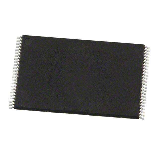
48-Lead TSOP (Normal Bend)
ETOXTM* Flash Technology
Not designed or rated as radiation hardened
The product is a low power, high density, low cost, nonvolatile read/write storage solution for a wide range of applications.
The product can operate at VCC=2.7V-3.6V. Its low voltage operation capability greatly extends battery life for portable
applications.
The memory array block architecture utilizes Enhanced Data Protection features, which provides maximum flexibility for
safe nonvolatile code and data storage.
Special OTP (One Time Program) block provides an area to store permanent code such as an unique number.
* ETOX is a trademark of Intel Corporation.
Rev. 2.45
�LHF00L28
A15
A14
A13
A12
A11
A10
A9
A8
A19
NC
WE#
RST#
NC
WP#/ACC
RY/BY#
A18
A17
A7
A6
A5
A4
A3
A2
A1
1
2
3
4
5
6
7
8
9
10
11
12
13
14
15
16
17
18
19
20
21
22
23
24
48-LEAD TSOP
STANDARD PINOUT
12mm x 20mm
TOP VIEW
3
48
47
46
45
44
43
42
41
40
39
38
37
36
35
34
33
32
31
30
29
28
27
26
25
A16
NC
GND
DQ15
DQ7
DQ14
DQ6
DQ13
DQ5
DQ12
DQ4
VCC
DQ11
DQ3
DQ10
DQ2
DQ9
DQ1
DQ8
DQ0
OE#
GND
CE#
A0
Figure 1. 48-Lead TSOP (Normal Bend) Pinout
Rev. 2.45
�LHF00L28
4
Table 1. Pin Descriptions
Symbol
Type
A19-A0
INPUT
DQ15-DQ0
INPUT/
OUTPUT
DATA INPUTS/OUTPUTS: Inputs data and commands during CUI (Command User
Interface) write cycles, outputs data during memory array, status register, query code,
identifier code reads. Data pins float to high-impedance (High Z) when the chip or
outputs are deselected. Data is internally latched during an erase or program cycle.
CE#
INPUT
CHIP ENABLE: Activates the device’s control logic, input buffers, decoders and sense
amplifiers. CE#-high (VIH) deselects the device and reduces power consumption to
standby levels.
RST#
INPUT
RESET: When low (VIL), RST# resets internal automation and inhibits write operations
which provides data protection. RST#-high (VIH) enables normal operation. After
power-up or reset mode, the device is automatically set to read array mode. RST# must
be low during power-up/down.
OE#
INPUT
OUTPUT ENABLE: Gates the device’s outputs during a read cycle.
INPUT
WRITE ENABLE: Controls writes to the CUI and array blocks. Addresses and data are
latched on the rising edge of CE# or WE# (whichever goes high first).
INPUT/
SUPPLY
WRITE PROTECT: When WP#/ACC is VIL, locked-down blocks cannot be unlocked.
Erase or program operation can be executed to the blocks which are not locked and not
locked-down. When WP#/ACC is VIH, lock-down is disabled.
Applying 12.0V±0.3V to WP#/ACC provides fast erasing or fast programming mode. In
this mode, WP#/ACC is power supply pin. Applying 12.0V±0.3V to WP#/ACC during
erase/program can only be done for a maximum of 1,000 cycles on each block. WP#/
ACC may be connected to 12.0V±0.3V for a total of 80 hours maximum. Use of this pin
at 12.0V+0.3V beyond these limits may reduce block cycling capability or cause
permanent damage.
WE#
WP#/ACC
RY/BY#
Name and Function
ADDRESS INPUTS: Inputs for addresses.
READY/BUSY#: Indicates the status of the internal WSM (Write State Machine). When
low, WSM is performing an internal operation (block erase, full chip erase, program or
OPEN DRAIN
OTP program). RY/BY#-High Z indicates that the WSM is ready for new commands,
OUTPUT
block erase is suspended and program is inactive, program is suspended, or the device is
in reset mode.
VCC
SUPPLY
DEVICE POWER SUPPLY (2.7V-3.6V): With VCC≤VLKO, all write attempts to the
flash memory are inhibited. Device operations at invalid VCC voltage (see DC
Characteristics) produce spurious results and should not be attempted.
GND
SUPPLY
GROUND: Do not float any ground pins.
NC
NO CONNECT: Lead is not internally connected; it may be driven or floated.
Rev. 2.45
�LHF00L28
5
[A19-A0]
FFFFF
FF000
FEFFF
FE000
FDFFF
FD000
FCFFF
FC000
FBFFF
FB000
FAFFF
FA000
F9FFF
F9000
F8FFF
F8000
F7FFF
F0000
EFFFF
E0000
DFFFF
D0000
CFFFF
C0000
BFFFF
B0000
AFFFF
A0000
9FFFF
90000
8FFFF
80000
7FFFF
70000
6FFFF
60000
5FFFF
50000
4FFFF
40000
3FFFF
30000
2FFFF
20000
1FFFF
10000
0FFFF
00000
4-Kword Block 23
4-Kword Block 22
4-Kword Block 21
4-Kword Block 20
4-Kword Block 19
4-Kword Block 18
4-Kword Block 17
4-Kword Block 16
32-Kword Block 15
64-Kword Block 14
64-Kword Block 13
64-Kword Block 12
64-Kword Block 11
64-Kword Block 10
64-Kword Block 9
64-Kword Block 8
64-Kword Block 7
64-Kword Block 6
64-Kword Block 5
64-Kword Block 4
64-Kword Block 3
64-Kword Block 2
64-Kword Block 1
64-Kword Block 0
Figure 2. Memory Map (Top Parameter)
Rev. 2.45
�LHF00L28
6
Table 2. Identifier Codes and OTP Address for Read Operation
Code
Address
[A19-A0]
Data
[DQ15-DQ0]
Manufacturer Code
Manufacturer Code
00000H
00B0H
Device Code
Device Code
00001H
00A4H
Block Lock Configuration
Code
Block is Unlocked
Block is Locked
Block is not Locked-Down
DQ0 = 0
1
DQ0 = 1
1
DQ1 = 0
1
DQ1 = 1
1
00080H
OTP-LK
2
00081-00088H
OTP
3
Block
Address
+2
Block is Locked-Down
OTP
OTP Lock
OTP
Notes
NOTES:
1. Block Address = The beginning location of a block address. DQ15-DQ2 are reserved for future implementation.
2. OTP-LK=OTP Block Lock configuration.
3. OTP=OTP Block data.
Rev. 2.45
�LHF00L28
7
[A19-A0]
000088H
Customer Programmable Area
000085H
000084H
Factory Programmed Area
000081H
000080H
Reserved for Future Implementation
(DQ15-DQ2)
Customer Programmable Area Lock Bit (DQ1)
Factory Programmed Area Lock Bit (DQ0)
Figure 3. OTP Block Address Map for OTP Program
(The area outside 80H~88H cannot be used.)
Rev. 2.45
�LHF00L28
8
Table 3. Bus Operation(1, 2)
Mode
Notes
RST#
CE#
OE#
WE#
Address
DQ15-0
RY/BY#
6
VIH
VIL
VIL
VIH
X
DOUT
High Z
Output Disable
VIH
VIL
VIH
VIH
X
High Z
X
Standby
VIH
VIH
X
X
X
High Z
X
(8)
Read Array
Reset
3
VIL
X
X
X
X
High Z
High Z
Read Identifier
Codes/OTP
6
VIH
VIL
VIL
VIH
See
Table 2
See
Table 2
High Z
Read Query
6,7
VIH
VIL
VIL
VIH
See
Appendix
See
Appendix
High Z
Read Status
Register
6
VIH
VIL
VIL
VIH
X
DOUT
X
4,5,6
VIH
VIL
VIH
VIL
X
DIN
X
Write
NOTES:
1. Refer to DC Characteristics for VIL or VIH voltages.
2. X can be VIL or VIH for control pins and addresses.
3. RST# at GND±0.2V ensures the lowest power consumption.
4. Command writes involving block erase, full chip erase, program or OTP program are reliably
executed when VCC=2.7V-3.6V.
5. Refer to Table 4 for valid DIN during a write operation.
6. Never hold OE# low and WE# low at the same timing.
7. Refer to Appendix of LHF00LXX series for more information about query code.
8. RY/BY# is VOL when the WSM (Write State Machine) is executing internal block erase, full chip erase, program or OTP
program algorithms. It is High Z during when the WSM is not busy, in block erase suspend mode (with program inactive),
program suspend mode, or reset mode.
Rev. 2.45
�LHF00L28
9
Table 4. Command Definitions(10)
Command
Read Array
Bus
Cycles
Req’d
First Bus Cycle
Notes
1
Second Bus Cycle
Oper(1)
Addr(2)
Data
Write
X
FFH
Oper(1)
Addr(2)
Data(3)
Read Identifier Codes/OTP
≥2
4
Write
X
90H
Read
IA or OA
ID or OD
Read Query
≥2
4
Write
X
98H
Read
QA
QD
Read
X
SRD
Read Status Register
2
Write
X
70H
Clear Status Register
1
Write
X
50H
Block Erase
2
5
Write
BA
20H
Write
BA
D0H
Full Chip Erase
2
5, 8
Write
X
30H
Write
X
D0H
2
5,6
Write
WA
40H or
10H
Write
WA
WD
Block Erase and
Program Suspend
1
7, 8
Write
X
B0H
Block Erase and
Program Resume
1
7, 8
Write
X
D0H
Set Block Lock Bit
2
Write
BA
60H
Write
BA
01H
Clear Block Lock Bit
2
Write
BA
60H
Write
BA
D0H
Set Block Lock-down Bit
2
Write
BA
60H
Write
BA
2FH
OTP Program
2
Write
OA
C0H
Write
OA
OD
Program
9
8
NOTES:
1. Bus operations are defined in Table 3.
2. All addresses which are written at the first bus cycle should be the same as the addresses which are written at the second
bus cycle.
X=Any valid address within the device.
IA=Identifier codes address (See Table 2).
QA=Query codes address. Refer to Appendix of LHF00LXX series for details.
BA=Address within the block being erased, set/cleared block lock bit or set block lock-down bit.
WA=Address of memory location for the Program command.
OA=Address of OTP block to be read or programmed (See Figure 3).
3. ID=Data read from identifier codes. (See Table 2).
QD=Data read from query database. Refer to Appendix of LHF00LXX series for details.
SRD=Data read from status register. See Table 8 for a description of the status register bits.
WD=Data to be programmed at location WA. Data is latched on the rising edge of WE# or CE# (whichever
goes high first) during command write cycles.
OD=Data within OTP block. Data is latched on the rising edge of WE# or CE# (whichever goes high first)
during command write cycles.
4. Following the Read Identifier Codes/OTP command, read operations access manufacturer code, device code, block lock
configuration code and the data within OTP block (See Table 2).
The Read Query command is available for reading CFI (Common Flash Interface) information.
5. Block erase, full chip erase or program cannot be executed when the selected block is locked. Unlocked block can be
erased or programmed when RST# is VIH.
6. Either 40H or 10H are recognized by the CUI (Command User Interface) as the program setup.
7. If the program operation and the erase operation are both suspended, the suspended program operation will be resumed
first.
8. Full chip erase and OTP program operations can not be suspended. The OTP Program command can not be accepted
while the block erase operation is being suspended.
Rev. 2.45
�LHF00L28
10
9. Following the Clear Block Lock Bit command, block which is not locked-down is unlocked when WP#/ACC is VIL.
When WP#/ACC is VIH, lock-down bit is disabled and the selected block is unlocked regardless of lock-down
configuration.
10. Commands other than those shown above are reserved by SHARP for future device implementations and should not be
used.
Rev. 2.45
�LHF00L28
11
Table 5. Functions of Block Lock(5) and Block Lock-Down
Current State
Erase/Program Allowed (2)
WP#/ACC
DQ1(1)
DQ0(1)
[000]
0
0
0
Unlocked
Yes
[001](3)
0
0
1
Locked
No
[011]
0
1
1
Locked-down
No
[100]
1
0
0
Unlocked
Yes
[101](3)
1
0
1
Locked
No
[110](4)
1
1
0
Lock-down Disable
Yes
[111]
1
1
1
Lock-down Disable
No
State
State Name
NOTES:
1. DQ0=1: a block is locked; DQ0=0: a block is unlocked.
DQ1=1: a block is locked-down; DQ1=0: a block is not locked-down.
2. Erase and program are general terms, respectively, to express: block erase, full chip erase and
program operations.
3. At power-up or device reset, all blocks default to locked state and are not locked-down, that is,
[001] (WP#/ACC=0) or [101] (WP#/ACC=1), regardless of the states before power-off or reset
operation.
4. When WP#/ACC is driven to VIL in [110] state, the state changes to [011] and the blocks are
automatically locked.
5. OTP (One Time Program) block has the lock function which is different from those described
above.
Table 6. Block Locking State Transitions upon Command Write(4)
Current State
Result after Lock Command Written (Next State)
State
WP#/ACC
DQ1
DQ0
Set Lock(1)
Clear Lock(1)
Set Lock-down(1)
[000]
0
0
0
[001]
No Change
[011](2)
[001]
0
0
1
No Change(3)
[000]
[011]
[011]
0
1
1
No Change
No Change
No Change
[100]
1
0
0
[101]
No Change
[111](2)
[101]
1
0
1
No Change
[100]
[111]
[110]
1
1
0
[111]
No Change
[111](2)
[111]
1
1
1
No Change
[110]
No Change
NOTES:
1. "Set Lock" means Set Block Lock Bit command, "Clear Lock" means Clear Block Lock Bit
command and "Set Lock-down" means Set Block Lock-Down Bit command.
2. When the Set Block Lock-Down Bit command is written to the unlocked block (DQ0=0), the
corresponding block is locked-down and automatically locked at the same time.
3. "No Change" means that the state remains unchanged after the command written.
4. In this state transitions table, assumes that WP#/ACC is not changed and fixed VIL or VIH.
Rev. 2.45
�LHF00L28
12
Table 7. Block Locking State Transitions upon WP#/ACC Transition(4)
Current State
Result after WP#/ACC Transition (Next State)
Previous State
[110]
(2)
State
WP#/ACC
DQ1
DQ0
WP#/ACC=0→1(1)
WP#/ACC=1→0(1)
[000]
0
0
0
[100]
-
[001]
0
0
1
[101]
-
[011]
0
1
1
[110]
-
[111]
-
Other than
[110](2)
-
[100]
1
0
0
-
[000]
-
[101]
1
0
1
-
[001]
-
[110]
1
1
0
-
[011](3)
-
[111]
1
1
1
-
[011]
NOTES:
1. "WP#/ACC=0→1" means that WP#/ACC is driven to VIH and "WP#/ACC=1→0" means that
WP#/ACC is driven to VIL.
2. State transition from the current state [011] to the next state depends on the previous state.
3. When WP#/ACC is driven to VIL in [110] state, the state changes to [011] and the blocks are
automatically locked.
4. In this state transitions table, assumes that lock configuration commands are not written in
previous, current and next state.
Rev. 2.45
�LHF00L28
13
Table 8. Status Register Definition
R
R
R
R
R
R
R
R
15
14
13
12
11
10
9
8
WSMS
BESS
BEFCES
POPS
WPACCS
PSS
DPS
R
7
6
5
4
3
2
1
0
SR.15 - SR.8 = RESERVED FOR FUTURE
ENHANCEMENTS (R)
SR.7 = WRITE STATE MACHINE STATUS (WSMS)
1 = Ready
0 = Busy
SR.6 = BLOCK ERASE SUSPEND STATUS (BESS)
1 = Block Erase Suspended
0 = Block Erase in Progress/Completed
SR.5 = BLOCK ERASE AND FULL CHIP ERASE
STATUS (BEFCES)
1 = Error in Block Erase or Full Chip Erase
0 = Successful Block Erase or Full Chip Erase
SR.4 = PROGRAM AND
OTP PROGRAM STATUS (POPS)
1 = Error in Program or OTP Program
0 = Successful Program or OTP Program
SR.3 = WP#/ACC STATUS (WPACCS)
1 = VCC+0.4V < WP#/ACC < 11.7V Detect,
Operation Abort
0 = WP#/ACC OK
SR.2 = PROGRAM SUSPEND
STATUS (PSS)
1 = Program Suspended
0 = Program in Progress/Completed
NOTES:
Status Register indicates the status of the WSM (Write State
Machine).
Check SR.7 or RY/BY# to determine block erase, full chip
erase, program or OTP program completion. SR.6 - SR.1 are
invalid while SR.7="0".
If both SR.5 and SR.4 are "1"s after a block erase, full chip
erase, program, set/clear block lock bit, set block lock-down
bit attempt, an improper command sequence was entered.
SR.3 does not provide a continuous indication of WP#/ACC
level. The WSM interrogates and indicates the WP#/ACC
level only after Block Erase, Full Chip Erase, Program or
OTP Program command sequences. SR.3 is not guaranteed to
report accurate feedback when WP#/ACC≠VACCH.
SR.1 does not provide a continuous indication of block lock
bit. The WSM interrogates the block lock bit only after Block
Erase, Full Chip Erase, Program or OTP Program command
sequences. It informs the system, depending on the attempted
operation, if the block lock bit is set. Reading the block lock
configuration codes after writing the Read Identifier Codes/
OTP command indicates block lock bit status.
SR.15 - SR.8 and SR.0 are reserved for future use and should
be masked out when polling the status register.
SR.1 = DEVICE PROTECT STATUS (DPS)
1 = Erase or Program Attempted on a
Locked Block, Operation Abort
0 = Unlocked
SR.0 = RESERVED FOR FUTURE ENHANCEMENTS
(R)
Rev. 2.45
�LHF00L28
1 Electrical Specifications
1.1 Absolute Maximum Ratings*
Operating Temperature
During Read, Erase and Program ...-40°C to +85°C (1)
Storage Temperature
During under Bias............................... -40°C to +85°C
During non Bias................................ -65°C to +125°C
Voltage On Any Pin (except VCC and WP#/ACC)
................................................. -0.5V to VCC+0.5V (2)
VCC Supply Voltage ........................... -0.2V to +3.9V (2)
WP#/ACC Supply Voltage ......... -0.2V to +12.6V (2, 3, 4)
Output Short Circuit Current ........................... 100mA (5)
14
*WARNING: Stressing the device beyond the "Absolute
Maximum Ratings" may cause permanent
damage. These are stress ratings only. Operation
beyond the "Operating Conditions" is not
recommended and extended exposure beyond the
"Operating Conditions" may affect device
reliability.
NOTES:
1. Operating temperature is for extended temperature
product defined by this specification.
2. All specified voltages are with respect to GND.
Minimum DC voltage is -0.5V on input/output pins and
-0.2V on VCC and WP#/ACC pins. During transitions,
this level may undershoot to -2.0V for periods