REFERENCE
�PC817X*NSZ1B
REFERENCE
1. These specification sheets include materials protected under copyright of Sharp Corporation ("Sharp").
Please handle with great cares and do not reproduce or cause anyone to reproduce them without Sharp's consent.
2. When using this Sharp product, please observe the absolute maximum ratings, other conditions and instructions for use
described in the specification sheets, as well as the precautions mentioned below.
Sharp assumes no responsibility for any damages resulting from use of the product which does not comply with absolute
maximum ratings, other conditions and instructions for use included in the specification sheets, and the precautions
mentioned below.
(Precautions)
(1) In making catalogue or instruction manual based on the specification sheets, please verify the validity of the catalogue
or instruction manuals after assembling Sharp products in customer's products at the responsibility of customer.
(2) This Sharp product is designed for use in the following application areas ;
• Computers • OA equipment • Telecommunication equipment (Terminal) • Measuring equipment
• Tooling machines ・Audio visual equipment • Home appliances
If the use of the Sharp product in the above application areas is for equipment listed in paragraphs (3) or (4),
please be sure to observe the precautions given in those respective paragraphs.
(3) Appropriate measures, such as fail-safe design and redundant design considering the safety design of the overall
system and equipment, should be taken to ensure reliability and safety when Sharp product is used for equipment
in responsibility of customer which demands high reliability and safety in function and precision, such as ;
• Transportation control and safety equipment (aircraft, train, automobile etc.)
• Traffic signals • Gas leakage sensor breakers • Rescue and security equipment
• Other safety equipment
(4)Sharp product is designed for consumer goods and controlled as consumer goods in production and quality.
Please do not use this product for equipment which require extremely high reliability and safety in function and
precision, such as ;
• Space equipment • Telecommunication equipment (for trunk lines)
• Nuclear power control equipment • Medical equipment
(5) Please contact and consult with a Sharp sales representative if there are any question regarding interpretation of
the above four paragraphs.
3. Disclaimer
The warranty period for Sharp product is one (1) year after shipment.
During the period, if there are any products problem, Sharp will repair (if applicable), replace or refund.
Except the above, both parties will discuss to cope with the problems.
The failed Sharp product after the above one (1) year period will be coped with by Sharp, provided that both parties
shall discuss and determine on sharing responsibility based on the analysis results thereof subject to the above scope
of warranty.
The warranty described herein is only for Sharp product itself which are purchased by or delivered to customer.
Damages arising from Sharp product malfunction or failure shall be excepted.
Sharp will not be responsible for the Sharp product due to the malfunction or failures thereof which are caused by:
(1) storage keep trouble during the inventory in the marketing channel.
(2) intentional act, negligence or wrong/poor handling.
(3) equipment which Sharp products are connected to or mounted in.
(4) disassembling, reforming or changing Sharp products.
(5) installation problem.
(6) act of God or other disaster (natural disaster, fire, flood, etc.)
(7) external factors (abnormal voltage, abnormal electromagnetic wave, fire, etc.)
(8) special environment (factory, coastal areas, hotspring area, etc.)
(9) phenomenon which cannot be foreseen based on the practical technologies at the time of shipment.
(10) the factors not included in the product specification sheet.
4. Please contact and consult with a Sharp sales representative for any questions about Sharp product.
1/10
�PC817X*NSZ1B
REFERENCE
1. Application
This specification applies to the outline and characteristics of photocoupler Model No. PC817series(Lead-Free Type).
2. Outline
Refer to the attached sheet, page 4.
3. Ratings and characteristics
Refer to the attached sheet, page 5, 6.
4. Reliability
Refer to the attached sheet, page 7.
5. Outgoing inspection
Refer to the attached sheet, page 8.
6. Supplement
6.1 Isolation voltage shall be measured in the following method.
(1) Short between anode and cathode on the primary side and between collector and emitter on the secondary side.
(2) The dielectric withstanding tester with zero-cross circuit shall be used.
(3) The wave form of applied voltage shall be a sine wave.
(It is recommended that the isolation voltage be measured in insulation oil.)
6.2 Package specifications
6.3 Business dealing name
Refer to the attached sheet, page 9, 10.
("○" mark indicates business dealing name of ordered product)
Rank mark
Ic (mA)
Test conditions
PC817XNNSZ1B
with or without
2.5 to 30
PC817X1NSZ1B
A
4.0 to 8.0
IF=5mA
VCE=5V
Ta=25℃
PC817X2NSZ1B
B
6.5 to 13
PC817X3NSZ1B
C
10 to 20
PC817X4NSZ1B
PC817X5NSZ1B
PC817X6NSZ1B
D
A or B
B or C
15 to 30
4.0 to 13
6.5 to 20
PC817X7NSZ1B
PC817X8NSZ1B
PC817X9NSZ1B
PC817X0NSZ1B
C or D
A, B or C
B, C or D
A, B, C or D
10 to 30
4.0 to 20
6.5 to 30
4.0 to 30
Ordered product Business dealing name
6.4 This Model is approved by UL. (Under preparation).
Approved Model No. : PC817
UL file No. : E64380
6.5 This Model is approved by CSA. (Under preparation).
Approved Model No. : PC817
CSA approved mark "
" shall be indicated on minimum unit package.
6.6 This product is not designed against irradiation.
This product is assembled with electrical input and output.
This product incorporates non-coherent light emitting diode.
2/10
�PC817X*NSZ1B
REFERENCE
6.7 ODS materials
This product shall not contain the following materials.
Also, the following materials shall not be used in the production process for this product.
Materials for ODS : CFCS, Halon, Carbon tetrachloride, 1.1.1-Trichloroethane (Methyl chloroform)
6.8 Specified brominated flame retardants
Specified brominated flame retardants (PBB and PBDE) are not used in this device at all.
6.9 Compliance with each regulation
(1) The RoHS directive(2011/65/EU)
This product complies with the RoHS directive(2011/65/EU) .
Object substances: mercury, lead, cadmium, hexavalent chromium, polybrominated biphenyls(PBB)
and polybrominated diphenyl ethers(PBDE)
(2) Content of six substances specified in Management Methods for Control of Pollution Caused by Electronic
Information Products Regulation (Chinese : 电子信息产品污染控制管理办法).
Category
Photocoupler
Marking Styles for the Names and Contents of the Hazardous Substances
Hazardous Substances
Hexavalent
Polybrominated
Lead
Mercury
Cadmium
chromium
biphenyls
(Pb)
(Hg)
(Cd)
6+
(Cr )
(PBB)
○
○
○
○
○
This table is prepared in accordance with the provisions of SJ/T 11364.
○:Indicates that said hazardous substance contained in all of the homogeneous materials for this part is
below the limit requirement of GB/T 26572
7. Notes
Precautions for photocouplers : Attachment-1.
3/10
Polybrominated
diphenyl ethers
(PBDE)
○
�PC817X*NSZ1B
REFERENCE
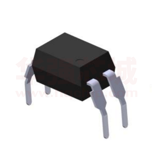
2. Outline
Anode mark
Rank mark
1.25 ± 0.15
Factory identification mark *2
Date code *1
④
4.60 ± 0.35
①
2.54 ± 0.25
Pin-Number and internal connection diagram
PC817
S
②
④ Collector
Anode ①
③ Emitter
Cathode ②
③
6.5 ± 0.5
Traceability code
0.25
3.2 ± 0.4
Epoxy resin
+0.1
-0.05
θ
θ
4.15 ± 0.4
3.5 ± 0.5
7.62 ± 0.30
0.5 ± 0.1
θ: 0~13°
*1) Date code : 3 digit indication according to production year and week
*2) Factory identification mark apply to the below
K : Kyushu Denshi Co.,Ltd. (Japan products)
Pin material : Copper Alloy
Pin finish
: SnBi plating (Bi : 1~4%)
Mark
: laser marking
Product mass : Approx. 0.23g
UNIT : 1/1 mm
Name
4/10
PC817 Outline Dimensions
(Business dealing name : PC817X*NSZ1B)
�PC817X*NSZ1B
REFERENCE
3. Ratings and characteristics
3.1 Absolute maximum ratings
Parameter
Input
Symbol
Rating
Unit
*1 Forward current
IF
50
mA
*2 Peak forward current
IFM
1
A
Reverse voltage
VR
6
V
P
70
mW
Collector-emitter voltage
VCEO
80
V
Emitter-collector voltage
VECO
6
V
Collector current
Ic
50
mA
*1 Collector power dissipation
Pc
150
mW
*1 Total power dissipation
Ptot
200
mW
Operating temperature
Topr
-30 to +100
℃
Storage temperature
Tstg
-55 to +125
℃
*1 Power dissipation
Output
Ta=25℃
*3 Isolation voltage
Viso(rms)
*4 Soldering temperature
Tsol
5
kV
270
℃
3.2 Electro-optical characteristics
Parameter
Ta=25℃
Symbol
Condition
MIN.
TYP.
MAX.
Unit
Forward voltage
VF
IF=20mA
-
1.2
1.4
V
Peak forward voltage
VFM
IFM=0.5A
-
-
3.0
V
Reverse current
IR
VR=4V
-
-
10
μA
Terminal capacitance
Ct
V=0, f=1kHz
-
30
250
pF
Dark current
ICEO
VCE=50V, IF=0
-
-
100
nA
Collector-emitter breakdown voltage
BVCEO
Ic=0.1mA IF=0
80
-
-
V
Emitter-collector breakdown voltage
BVECO
IE=10μA, IF=0
6
-
-
V
Collector current
Ic
IF=5mA, VCE=5V
2.5
-
30
mA
Collector-emitter saturation voltage
VCE(sat)
IF=20mA Ic=1mA
-
0.1
0.2
V
Isolation resistance
RISO
DC500V 40 to 60%RH
5×10¹⁰
1011
-
Ω
Transfer Floating capacitance
characteristics Cut-off frequency
Cf
V=0, f=1MHz
-
0.6
1.0
pF
fc
VCE=5V, Ic=2mA
RL=100Ω, -3dB
-
80
-
kHz
Rise time
tr
-
4
18
μs
Fall time
tf
-
3
18
μs
Input
Output
*1
*2
*3
*4
VCE=2V Ic=2mA
RL=100Ω
The derating factors of absolute maximum ratings due to ambient temperature are shown in Fig. 1 to 4.
Pulse width≦100μs, Duty ratio : 0.001 (Refer to Fig. 5)
AC for 1 min, 40 to 60%RH
For 10 s
5/10
�PC817X*NSZ1B
REFERENCE
(Fig.2) Diode power dissipation
vs. ambient temperature
Diode power dissipation P (mW)
(Fig.1) Forward current
vs. ambient temperature
Forward current IF (mA)
50
40
30
20
10
0
-30 -25
0
25
50
55
75
100
125
100
80
70
60
40
20
0
-30 -25
Ambient temperature Ta (℃)
Total power dissipation Ptot (mW)
Collector power dissipation Pc (mW)
200
150
100
50
25
50
75
100
125
Ambient temperature Ta (℃)
Peak forward current IFM (mA)
2000
1000
500
200
100
50
20
10 -3
10 -2
75
100
125
10 -1
250
200
150
100
50
0
-30 -25
0
25
50
75
100
Ambient temperature Ta (℃)
(Fig.5) Peak forward current vs. duty ratio
Pulse width ≦ 100μs
Ta = 25℃
10
50 55
(Fig.4) Total power dissipation
vs. ambient temperature
250
0
25
Ambient temperature Ta (℃)
(Fig.3) Collector power dissipation
vs. ambient temperature
0
-30 -25
0
10 0
Duty ratio
6/10
125
�PC817X*NSZ1B
REFERENCE
4. Reliability
The reliability of products shall satisfy items listed below.
Confidence level : 90%
LTPD : 10 or 20
Test Items
Solderability
Failure Judgment
Criteria
Condition
245±3ºC, 5s
Soldering heat
*2
(Flow soldering) 270ºC, 10 s
Samples (n)
Defective (C)
n=11, C=0
n=11, C=0
(Soldering by hand) 400ºC, 3 s
VF
>U×1.2
IR
>U×2
ICEO >U×2
IC
<L×0.7
VCE(sat) >U×1.2
Terminal strength
(Tension)
Weight: 5N 5 s/each terminal
Terminal strength
(Bending) *3
Weight: 2.5N 2 times/each terminal
Mechanical shock
15km/s2, 0.5ms
3 times/±X, ±Y, ±Z direction
Variable frequency
vibration
100 to 2000 to 100Hz/4 min 200m/s2
4 times/X, Y, Z direction
Temperature cycling
1 cycle –55 ºC to +125 ºC
(30 min) (30 min)
20 cycles test
High temp. and high
Humidity storage
+85ºC, 85%RH, 1000h
n=22, C=0
High temp. storage
+125 ºC, 1000h
n=22, C=0
Low temp. storage
-55 ºC, 1000h
n=22, C=0
Operation life
IF=50mA, Ptot=200mW
Ta=25 ºC, 1000h
n=22, C=0
n=11, C=0
n=11, C=0
U: Upper specification limit
L: Lower specification limit
n=11, C=0
n=22, C=0
*1 Test method, conforms to EIAJ ED 4701.
*2 The product whose not-soldered area is more than 5% for all of the dipped area,
and/or whose pinholes or voids are concentrated on one place shall be judged defect.
*3 Terminal bending direction is shown below.
θ
n=11, C=0
θ
7/10
�PC817X*NSZ1B
REFERENCE
5. Outgoing inspection
5.1 Inspection items
(1) Electrical characteristics
VF, IR, ICEO, VCE(sat), Ic, RISO, Viso
(2) Appearance
5.2 Sampling method and Inspection level
LTPD sampling inspection
confidence level:90%
Defect
Inspection item
LTPD(%)
Major defect
Electrical characteristics(faiure)
Marking (Unreadable)
Lead form (Deformation)
3
Appearance defect except
Minor defect
50
the above mentioned.
8/10
�PC817X*NSZ1B
REFERENCE
6.2 Package specification
6.2.1 Package materials
No.
Name
Purposes
①
Sleeve
②
Stopper
Enhanced polymer
Products fixed
③
Inner bag
Polyethylene
Packaging bag for sleeve with product
④
Sealing tape
Cellophane
Lid of inner bag
⑤
Label
Paper
Model No.,(Business dealing name),Lot No.,
Quantity, Country of origin , Company name
and Inspection date specified
⑥
Packing case
Paper
Inner bag packaged
⑦
Cushioning material
Polyethylene
Inner bag fixed
⑧
Sealing tape
Cellophane
Lid of packingcase
Paper
Model No.,(Business dealing name),Lot No.,
Quantity, Country of origin , Company name
and Inspection date specified
⑨ Label
6.2.2
(1)
(2)
(3)
(4)
(5)
(6)
Materials
HIPS or ABS with preventing
Products packaged
static electricity
Package method
MAX. 100pcs. of products shall be packaged in a sleeve ① and both of sleeve edges shall be fixed by stoppers ②.
MAX. 25 sleeves (Product : 2500pcs.) above shall be packaged in inner case ③. and sealed by tape ④.
The label ⑤ shall be put on the top of the inner bag.
Max 2 bags(product : 5000pcs) above shall be packaged in packing case ⑥, and put a cushioning material ⑦ inside.
The label ⑨ shall be put on the side of the packing case.
Case shall be closed with the lid and enclosed with kraft tape ⑧.
6.2.3 Sleeve package ① outline dimensions
11.1 ± 0.2
5.5 ± 0.2
6.5 ± 0.2
8.8 ± 0.2
6.5 ± 0.2
14.2 ± 0.2
500 ± 2
(Unit :mm)
Note 1) Thickness : 0.5±0.2mm
2) Process with applying antistatic treatment.
3) Unless otherwise specified tolerances shall be ±0.5mm.
(However except for deformation due to the stopper in sleeve.)
9/10
�PC817X*NSZ1B
REFERENCE
6.2.4 Packing outer case outline dimensions
Sleeve①
Product
Anode mark
Stopper②
Anode mark shall be arranged at stopper side without pulled portion.
Stopper②
Sealing tape④
Label⑤
Inner bag③
Cushioning material⑦
(535mm)
Sealing tape⑧
Packing case⑥
(180mm)
(85mm)
Label⑨
Regular packing mass : Approx. 2kg
( ) : Reference dimensions
10/10
�PC817X*NSZ1B
REFERENCE
Precautions for Photocouplers
1 Cleaning
(1) Solvent cleaning : Solvent temperature 45℃ or less
Immersion for 3 min or less
(2) Ultrasonic cleaning : The effect to device by ultrasonic cleaning differs by cleaning bath size, ultrasonic power output,
cleaning time, PCB size or device mounting condition etc. Please test it in actual using condition
and confirm that any defect doesn't occur before starting the ultrasonic cleaning.
(3) Applicable solvent : Ethyl alcohol, Methyl alcohol, Isopropyl alcohol
When the other solvent is used, there are cases that the packaging resin is eroded.
Please use the other solvent after thorough confirmation is performed in actual using condition.
2. Circuit design
2.1 The LED used in the Photocoupler generally decreases the light emission power by operation.
In case of long operation time, please design the circuit in consideration of the degradation
of the light emission power of the LED. (50%/5years)
2.2 There are cases that the deviation of the CTR and the degradation of the relative light emission power
of the LED increase when the setting value of IF is less than 1.0mA. Please design the circuit in consideration of this point.
3. Precautions for Soldering
(1) In the case of flow soldering (Whole dipping is possible)
It is recommended that flow soldering should be at 270℃ or less for 10 s or less
(Pre-heating : 100 to 150℃, 30 to 80s). (2 times or less)
(2) In the case of hand soldering
What is done on the following condition is recommended.( 2 times or less)
Soldering iron temperature : 400℃ or less
Time : 3s or less
(3) Other precautions
Depending on equipment and soldering conditions (temperature, Using solder etc.),
the effect to the device and the PCB is different.
Please confirm that there is no problem on the actual use conditions in advance.
Attachment-1.
�Mouser Electronics
Authorized Distributor
Click to View Pricing, Inventory, Delivery & Lifecycle Information:
Sharp Microelectronics:
PC817X3NSZ1B PC817X1NSZ1B PC817X4NSZ1B PC817X2NSZ1B
�