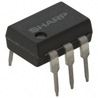
PC900V0NSZX Series
PC900V0NSZX
Series
Digital Output, Normal OFF
Operation DIP 6 pin ∗OPIC
Photocoupler
■ Description
■ Agency approvals/Compliance
PC900V0NSZX Series contains an IRED optically
coupled to an OPIC chip.
It is packaged in a 6 pin DIP, available in SMT gullwing lead-form and Wide SMT gullwing lead-form option.
Input-output isolation voltage(rms) is 5.0kV.
1. Recognized by UL1577 (Double protection isolation),
file No. E64380 (as model No. PC900V)
2. Approved by TÜV (VDE0884) (as an option) file No.
R9151577 (as model No. PC900V)
3. Package resin : UL flammability grade (94V-0)
■ Applications
■ Features
1. Programmable controllers
2. PC peripherals
3. Electronic musical instruments
1. 6 pin DIP package
2. Double transfer mold package
(Ideal for Flow Soldering)
3. Normal OFF operation, open collector output
4. TTL and LSTTL compatible output
5. Operating supply voltage (VCC : 3 to 15 V)
6. Isolation voltage (Viso(rms) : 5.0 kV)
∗ "OPIC"(Optical IC) is a trademark of the SHARP Corporation. An OPIC consists of a light-detecting element and a signal-processing
circuit integrated onto a single chip.
Notice The content of data sheet is subject to change without prior notice.
In the absence of confirmation by device specification sheets, SHARP takes no responsibility for any defects that may occur in equipment using any SHARP
devices shown in catalogs, data books, etc. Contact SHARP in order to obtain the latest device specification sheets before using any SHARP device.
1
Sheet No.: D2-A05301EN
Date Nov. 28. 2003
© SHARP Corporation
�PC900V0NSZX Series
■ Internal Connection Diagram
6
5
4
1
2
Voltage
regulator
3
Amp
4
5
1
2
6
3
Anode
Cathode
NC
VO
GND
VCC
■ Outline Dimensions
(Unit : mm)
1. Through-Hole [ex. PC900V0NSZX]
2. Through-Hole (VDE0884 option) [ex. PC900V0YSZX]
1.2±0.3
1.2±0.3
0.6±0.2
SHARP
mark
"S"
4
PC900V
Anode
mark
1
2
6
7.12
1
Date code
2
3
±0.5
7.12
3.5±0.5
7.62±0.3
2.9±0.5
0.5TYP.
7.62±0.3
3.5±0.5
VDE0884 Identification mark
4
±0.5
2.9±0.5
4
PC900V
Anode
mark
Date code
3
5
Epoxy resin
θ : 0 to 13˚
3. SMT Gullwing Lead-Form [ex. PC900V0NIPX]
6
4
PC900V
Anode
mark
SHARP
mark
"S"
PC900V
4
3
Date code
1
7.12±0.5
Epoxy resin
3
7.62±0.3
3.5±0.5
0.26±0.1
1.0+0.4
−0
2
7.12±0.5
7.62±0.3
3.5±0.5
2.54±0.25
VDE0884 Identification mark
0.35±0.25
2
4
Anode
mark
Date code
1
5
2.54±0.25
1.0+0.4
−0
10.0+0
−0.5
0.26±0.1
5
θ
θ : 0 to 13˚
1.2±0.3
0.6±0.2
6.5±0.5
6
SHARP
mark
"S"
θ
4. SMT Gullwing Lead-Form (VDE0884 option)
[ex. PC900V0YIPX]
1.2±0.3
0.6±0.2
0.5±0.1
2.54±0.25
θ
3.25±0.5
θ
6.5±0.5
0.5±0.1
2.54±0.25
3.25±0.5
Epoxy resin
0.35±0.25
5
0.5TYP.
6
6.5±0.5
SHARP
mark
"S"
6.5±0.5
0.6±0.2
1.0+0.4
−0
Epoxy resin
1.0+0.4
−0
10.0+0
−0.5
Sheet No.: D2-A05301EN
2
�PC900V0NSZX Series
(Unit : mm)
1.2±0.3
PC900V
Anode
mark
1.2±0.3
0.6±0.2
SHARP
mark
"S"
6.5±0.5
0.6±0.2
SHARP
mark
"S"
6. Wide SMT Gullwing Lead-Form (VDE0884 option)
[ex. PC900V0YUPX]
PC900V
4
Anode
mark
Date code
6.5±0.5
5. Wide SMT Gullwing Lead-Form
[ex. PC900V0NUPX]
Date code
VDE0884 Identification mark
0.75±0.25
Epoxy resin
10.16±0.5
12.0MAX.
2.54±0.25
0.75±0.25
7.62±0.3
0.25±0.25
3.5±0.5
0.25±0.25
7.62
0.26±0.1
3.5±0.5
2.54±0.25
7.12±0.5
±0.3
0.26±0.1
7.12±0.5
0.75±0.25
Epoxy resin
10.16±0.5
12.0MAX.
0.75±0.25
Product mass : approx. 0.36g
Sheet No.: D2-A05301EN
3
�PC900V0NSZX Series
Date code (2 digit)
A.D.
1990
1991
1992
1993
1994
1995
1996
1997
1998
1999
2000
2001
1st digit
Year of production
A.D
Mark
2002
A
2003
B
2004
C
2005
D
2006
E
2007
F
2008
H
2009
J
2010
K
2011
L
2012
M
··
N
·
Mark
P
R
S
T
U
V
W
X
A
B
C
··
·
2nd digit
Month of production
Month
Mark
January
1
February
2
March
3
April
4
May
5
June
6
July
7
August
8
September
9
October
O
November
N
December
D
repeats in a 20 year cycle
Country of origin
Japan
Sheet No.: D2-A05301EN
4
�PC900V0NSZX Series
■ Absolute Maximum Ratings
Parameter
Symbol
IF
Forward current
*1
Peak forward current
IFM
Input
Reverse voltage
VR
Power dissipation
P
Supply voltage
VCC
High level output voltage
VOH
Output
Low level output current
IOL
PO
Power dissipation
Ptot
Total power dissipation
Topr
Operating temperature
Storage temperature
Tstg
*2
Isolation voltage
Viso (rms)
*3
Soldering temperature
Tsol
Rating
50
1
6
70
16
16
50
150
170
−25 to +85
−40 to +125
5.0
260
(Ta=25˚C)
Unit
mA
A
V
mW
V
V
mA
mW
mW
˚C
˚C
kV
˚C
*1 Pulse width≤100µs, Duty ratio : 0.001
*2 40 to 60%RH, AC for 1minute, f=60Hz
*3 For 10s
■ Electro-optical Characteristics
Output
Input
Parameter
Forward voltage
Reverse current
Terminal capacitance
Operating Supply voltage
Low level output voltage
High level output current
Low level supply current
High level supply current
*4
"High→Low" input
threshold current
*5
Transfer characteristics
VF
IR
Ct
VCC
VOL
IOH
ICCL
ICCH
IFHL
IFLH
IFLH/IFHL
Hysteresis
RISO
Isolation voltage
tPHL
"High→Low" propagation delay time
"Low→High" propagation delay time
tPLH
Rise time
tr
Fall time
tf
Response time
*6
"Low→High" input
threshold current
Symbol
Conditions
IF=4mA
IF=0.3mA
Ta=25˚C, VR=3V
Ta=25˚C, V=0, f=1kHz
−
IOL=16mA, VCC=5V, IF=4mA
VO=VCC=15V, IF=0
VCC=5V, IF=4mA
VCC=5V, IF=0
Ta=25˚C, VCC=5V, RL=280Ω
VCC=5V, RL=280Ω
Ta=25˚C, VCC=5V, RL=280Ω
VCC=5V, RL=280Ω
VCC=5V, RL=280Ω
Ta=25˚C, DC500V, 40 to 60%RH
Ta=25˚C, VCC=5V, IF=4mA
RL=280Ω
(Unless otherwise specified Ta=0 to +70˚C)
MIN.
MAX.
TYP.
Unit
−
1.1
1.4
V
−
0.7
1.0
−
−
10
µA
30
−
250
pF
3
−
15
V
0.2
−
0.4
V
−
−
100
µA
−
2.5
5.0
mA
1.0
−
5.0
mA
1.1
−
2.0
mA
−
−
4.0
0.8
0.4
−
mA
0.3
−
−
0.7
−
0.5
0.9
1×10¹¹
5×10¹⁰
−
Ω
1
−
3
2
−
6
µs
−
0.1
0.5
−
0.05
0.5
*4 IFHL represents forward current when output goes from high to low.
*5 IFLH represents forward current when output goes from low to high.
*6 Hysteresis stands for IFLH/IFHL.
Sheet No.: D2-A05301EN
5
�PC900V0NSZX Series
■ Model Line-up
SMT Gullwing
Wide SMT Gullwing
Sleeve
Taping
Package
50pcs/sleeve
1 000pcs/reel
−−−−−−
Approved
−−−−−−
Approved
−−−−−−
Approved
−−−−−−
Approved
VDE0884
Model No. PC900V0NSZX PC900V0YSZX PC900V0NIZX PC900V0YIZX PC900V0NIPX PC900V0YIPX PC900V0NUPX PC900V0YUPX
Lead Form
Through-Hole
Please contact a local SHARP sales representative to inquire about production status and Lead-Free options.
Sheet No.: D2-A05301EN
6
�PC900V0NSZX Series
Fig.1 Test Circuit for Response Time
Voltage
regulator
tPHL
280Ω
tr=tf=0.01µs
ZO=50Ω
50%
VIN
5V
Amp
VIN
tPLH
VO
0.1µF
47Ω
VOH
90%
1.5V
10%
VOL
tr
VO
tf
Fig.3 Power Dissipation vs. Ambient
Temperature
60
200
50
170
Power dissipation PO, Ptot (mW)
Forward current IF (mA)
Fig.2 Forward Current vs. Ambient
Temperature
40
30
20
Ptot
PO
150
100
50
10
0
−25
0
25
50
75 85
0
−25
100
Ambient temperature Ta (˚C)
1.4
Forward current IF (mA)
Relative input threshold current IFHL, IFLH
Ta=75˚C
50˚C
25˚C
0˚C
−25˚C
50
50
75 85
100
Fig.5 Relative Input Threshold Current vs.
Supply Voltage
500
100
25
Ambient temperature Ta (˚C)
Fig.4 Forward Current vs. Forward Voltage
200
0
20
10
5
2
Ta=25˚C
IFHL=1 at VCC=5V
1.2
IFHL
1.0
IFLH
0.8
0.6
0.4
0.2
1
0
0.5
1.0
1.5
2.0
2.5
0
3.0
5
10
15
20
Supply voltage VCC (V)
Forward voltage VF (V)
Sheet No.: D2-A05301EN
7
�PC900V0NSZX Series
Fig.7 Low Level Output Voltage vs. Low
Level Output Current
Fig.6 Relative Input Threshold Current vs.
Ambient Temperature
1.0
VCC=5V
VCC=5V
1.4
Low level output voltage VOL (V)
Relative input threshold current IFHL, IFLH
1.6
1.2
IFHL
1.0
0.8
IFLH
0.6
0.4
Ta=25˚C
0.5
0.2
0.1
0.05
0.02
0.2
−25
IFHL=1 at Ta=25˚C
0
25
50
0.01
75
100
1
2
Ambient temperature Ta (˚C)
20
9
0.5
IOL=30mA
VCC=5V
50
0.4
Ta= −25˚C
25˚C
7
0.3
16mA
0.2
5mA
0.1
0
−25
0
25
50
6
5
4
2
75
85˚C
5
7
9
11
13
15
17
Supply voltage VCC (V)
Fig.11 Rise Time, Fall Time vs. Load
Resistance
Fig.10 Propagation Delay Time vs. Forward
Current
0.5
Rise time, fall time tr, tf (µs)
VCC=5V
RL=280Ω
Ta=25˚C
4
25˚C
ICCL{
1 I
CCH{
0
1
3
100
Ta= −25˚C
85˚C
3
Ambient temperature Ta (˚C)
5
100
8
Supply current ICC (mA)
Low level output voltage VOL (V)
10
Fig.9 Supply Current vs. Supply Voltage
Fig.8 Low Level Output Voltage vs. Ambient
Temperature
Propagation delay time tPHL, tPLH (µs)
5
Low level output current IOL (mA)
tPLH
3
2
1
0.4
VCC=5V
IF=4mA
Ta=25˚C
0.3
0.2
tr
0.1
tf
tPHL
0
0
10
20
30
40
50
0
0.1
60
Forward current IF (mA)
0.2
0.5
1
2
5
10
20
Load resistance RL (kΩ)
Remarks : Please be aware that all data in the graph are just for reference and not for guarantee.
Sheet No.: D2-A05301EN
8
�PC900V0NSZX Series
■ Design Considerations
● Notes about static electricity
Transistor of detector side in bipolar configuration may be damaged by static electricity due to its minute design.
When handling these devices, general countermeasure against static electricity should be taken to avoid
breakdown of devices or degradation of characteristics.
● Design guide
In order to stabilize power supply line, we should certainly recommend to connect a by-pass capacitor of
0.01µF or more between VCC and GND near the device.
The detector which is used in this device, has parasitic diode between each pins and GND.
There are cases that miss operation or destruction possibly may be occurred if electric potential of any pin
becomes below GND level even for instant.
Therefore it shall be recommended to design the circuit that electric potential of any pin does not become
below GND level.
This product is not designed against irradiation and incorporates non-coherent IRED.
● Degradation
In general, the emission of the IRED used in photocouplers will degrade over time.
In the case of long term operation, please take the general IRED degradation (50% degradation over 5years)
into the design consideration.
Please decide the input current which become 2times of MAX. IFHL.
Sheet No.: D2-A05301EN
9
�PC900V0NSZX Series
● Recommended Foot Print (reference)
SMT Gullwing Lead-form
Wide SMT Gullwing Lead-form
10.5
1.7
1.7
2.54
2.54
2.54
2.54
8.5
2.2
2.2
(Unit : mm)
✩ For additional design assistance, please review our corresponding Optoelectronic Application Notes.
Sheet No.: D2-A05301EN
10
�PC900V0NSZX Series
■ Manufacturing Guidelines
● Soldering Method
Reflow Soldering:
Reflow soldering should follow the temperature profile shown below.
Soldering should not exceed the curve of temperature profile and time.
Please don't solder more than twice.
(˚C)
300
Terminal : 260˚C peak
( package surface : 250˚C peak)
200
Reflow
220˚C or more, 60s or less
Preheat
150 to 180˚C, 120s or less
100
0
0
1
2
3
4
(min)
Flow Soldering :
Due to SHARP's double transfer mold construction submersion in flow solder bath is allowed under the below
listed guidelines.
Flow soldering should be completed below 270˚C and within 10s.
Preheating is within the bounds of 100 to 150˚C and 30 to 80s.
Please don't solder more than twice.
Hand soldering
Hand soldering should be completed within 3s when the point of solder iron is below 400˚C.
Please don't solder more than twice.
Other notices
Please test the soldering method in actual condition and make sure the soldering works fine, since the impact
on the junction between the device and PCB varies depending on the tooling and soldering conditions.
Sheet No.: D2-A05301EN
11
�PC900V0NSZX Series
● Cleaning instructions
Solvent cleaning:
Solvent temperature should be 45˚C or below Immersion time should be 3minutes or less
Ultrasonic cleaning:
The impact on the device varies depending on the size of the cleaning bath, ultrasonic output, cleaning time,
size of PCB and mounting method of the device.
Therefore, please make sure the device withstands the ultrasonic cleaning in actual conditions in advance of
mass production.
Recommended solvent materials:
Ethyl alcohol, Methyl alcohol and Isopropyl alcohol
In case the other type of solvent materials are intended to be used, please make sure they work fine in actual using conditions since some materials may erode the packaging resin.
● Presence of ODC
This product shall not contain the following materials.
And they are not used in the production process for this device.
Regulation substances : CFCs, Halon, Carbon tetrachloride, 1.1.1-Trichloroethane (Methylchloroform)
Specific brominated flame retardants such as the PBBOs and PBBs are not used in this product at all.
Sheet No.: D2-A05301EN
12
�PC900V0NSZX Series
■ Package specification
● Sleeve package
Package materials
Sleeve : HIPS (with anti-static material)
Stopper : Styrene-Elastomer
Package method
MAX. 50 pcs. of products shall be packaged in a sleeve.
Both ends shall be closed by tabbed and tabless stoppers.
The product shall be arranged in the sleeve with its anode mark on the tabless stopper side.
MAX. 20 sleeves in one case.
Sleeve outline dimensions
12.0
±2
5.8
10.8
520
6.7
(Unit : mm)
Sheet No.: D2-A05301EN
13
�PC900V0NSZX Series
● Tape and Reel package
1. SMT Gullwing
Package materials
Carrier tape : A-PET (with anti-static material)
Cover tape : PET (three layer system)
Reel : PS
Carrier tape structure and Dimensions
F
D
J
G
I
5˚
MA
X.
H
H
A
B
C
E
K
Dimensions List
A
B
±0.3
16.0
7.5±0.1
H
I
±0.1
10.4
0.4±0.05
C
1.75±0.1
J
4.2±0.1
D
12.0±0.1
K
7.8±0.1
E
2.0±0.1
F
4.0±0.1
(Unit:mm)
G
+0.1
φ1.5−0
Reel structure and Dimensions
e
d
c
g
Dimensions List
a
b
330
17.5±1.5
e
f
±1.0
23
2.0±0.5
f
a
b
(Unit : mm)
c
d
100±1.0
13±0.5
g
2.0±0.5
Direction of product insertion
Pull-out direction
[Packing : 1 000pcs/reel]
Sheet No.: D2-A05301EN
14
�PC900V0NSZX Series
2. Wide SMT Gullwing
Package materials
Carrier tape : A-PET (with anti-static material)
Cover tape : PET (three layer system)
Reel : PS
Carrier tape structure and Dimensions
F
D
G
E
I
J
MA
X.
H
H
A
B
C
Dimensions List
A
B
24.0±0.3
11.5±0.1
H
I
±0.1
12.2
0.4±0.05
5˚
K
C
1.75±0.1
J
4.1±0.1
D
12.0±0.1
K
7.6±0.1
E
2.0±0.1
(Unit : mm)
F
G
+0.1
4.0±0.1
φ1.5−0
Reel structure and Dimensions
e
d
c
g
Dimensions List
a
b
a
330
e
23±1.0
f
b
25.5±1.5
f
2.0±0.5
(Unit : mm)
c
d
±1.0
100
13±0.5
g
2.0±0.5
Direction of product insertion
Pull-out direction
[Packing : 1 000pcs/reel]
Sheet No.: D2-A05301EN
15
�PC900V0NSZX Series
■ Important Notices
with equipment that requires higher reliability such as:
--- Transportation control and safety equipment (i.e.,
aircraft, trains, automobiles, etc.)
--- Traffic signals
--- Gas leakage sensor breakers
--- Alarm equipment
--- Various safety devices, etc.
(iii) SHARP devices shall not be used for or in connection with equipment that requires an extremely high level of reliability and safety such as:
--- Space applications
--- Telecommunication equipment [trunk lines]
--- Nuclear power control equipment
--- Medical and other life support equipment (e.g.,
scuba).
· The circuit application examples in this publication are
provided to explain representative applications of
SHARP devices and are not intended to guarantee any
circuit design or license any intellectual property rights.
SHARP takes no responsibility for any problems related to any intellectual property right of a third party resulting from the use of SHARP's devices.
· Contact SHARP in order to obtain the latest device
specification sheets before using any SHARP device.
SHARP reserves the right to make changes in the specifications, characteristics, data, materials, structure,
and other contents described herein at any time without
notice in order to improve design or reliability. Manufacturing locations are also subject to change without notice.
· If the SHARP devices listed in this publication fall within the scope of strategic products described in the Foreign Exchange and Foreign Trade Law of Japan, it is
necessary to obtain approval to export such SHARP devices.
· Observe the following points when using any devices
in this publication. SHARP takes no responsibility for
damage caused by improper use of the devices which
does not meet the conditions and absolute maximum
ratings to be used specified in the relevant specification
sheet nor meet the following conditions:
(i) The devices in this publication are designed for use
in general electronic equipment designs such as:
--- Personal computers
--- Office automation equipment
--- Telecommunication equipment [terminal]
--- Test and measurement equipment
--- Industrial control
--- Audio visual equipment
--- Consumer electronics
(ii) Measures such as fail-safe function and redundant
design should be taken to ensure reliability and safety
when SHARP devices are used for or in connection
· This publication is the proprietary product of SHARP
and is copyrighted, with all rights reserved. Under the
copyright laws, no part of this publication may be reproduced or transmitted in any form or by any means, electronic or mechanical, for any purpose, in whole or in
part, without the express written permission of SHARP.
Express written permission is also required before any
use of this publication may be made by a third party.
· Contact and consult with a SHARP representative if
there are any questions about the contents of this publication.
Sheet No.: D2-A05301EN
16
�