1. 物料型号:文档中提到了PQxxxEH02ZxH系列,具体型号包括PQ015EH02ZPH、PQ018EH02ZPH、PQ025EH02ZPH(Taping封装)和PQ015EH02ZZH、PQ018EH02ZZH、PQ025EH02ZZH(Sleeve封装)。
2. 器件简介:PQxxxEH02ZxH系列是低电压操作、低功耗的电压调节器。特点包括低电压操作(最小工作电压2.35V)、大输出电流型(IO: 2A)、低耗散电流、低功耗、内置过流和过热保护功能、TO-263封装、符合RoHS指令。
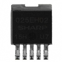
3. 引脚分配:文档中提供了引脚分配图,包括DC输入(VIN)、ON/OFF控制端(VC)、DC输出(VO)、NC(空脚)、GND(地)。
4. 参数特性:文档列出了电气特性,包括输入电压范围、输出电压、负载调整率、线路调整率、输出电压的温度系数、纹波抑制、控制端的ON/OFF状态电压和电流、静态电流等。
5. 功能详解:文档中详细描述了器件的功能特性,如低功耗运行、过流和过热保护、输出电压的稳定性等。
6. 应用信息:PQxxxEH02ZxH系列适用于个人电脑及其外围设备、各种数字电子设备的电源供应,如DVD播放器或机顶盒、汽车设备的电源供应,如车载导航系统。
7. 封装信息:器件提供Taping和Sleeve两种封装类型,引脚完成为无铅焊料镀层(成分:Sn2Cu)。