物料型号:
- PQ015EZ5MZPH/PQ015EZ5MZZH
- PQ018EZ5MZPH/PQ018EZ5MZZH
- PQ025EZ5MZPH/PQ025EZ5MZZH
- PQ030EZ5MZPH/PQ030EZ5MZZH
- PQ033EZ5MZPH/PQ033EZ5MZZH
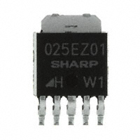
- PQ015EZ01ZPH/PQ015EZ01ZZH
- PQ018EZ01ZPH/PQ018EZ01ZZH
- PQ025EZ01ZPH/PQ025EZ01ZZH
- PQ030EZ01ZPH/PQ030EZ01ZZH
- PQ033EZ01ZPH/PQ033EZ01ZZH
器件简介:
这些是紧凑型表面贴装式低压降电压调节器,具有低电压运行(最小工作电压:2.35V)、低耗散电流、内置过流保护和过热保护功能,并且符合RoHS指令。
引脚分配:
1. DC输入(VIN)
2. ON/OFF控制端(VC)
3. DC输出(VO)
4. 不连接(NC)
5. 地(GND)
参数特性:
- 输入电压范围:2.35V至10V
- 输出电流:0.5A或1A
- 功耗:最大8W
- 工作温度:-40至+85°C
- 存储温度:-40至+150°C
- 焊接温度:260°C(10s)
功能详解:
这些电压调节器提供了过流保护和过热保护,确保在过热时可以自动降低输出电流或关闭输出以保护器件。
应用信息:
适用于个人电脑外围设备、DVD播放器或STB等各种电子设备的电源。
封装信息:
提供Taping(卷带)和Sleeve(管装)封装类型,具体封装尺寸图在文档中有详细描述。