PQ035ZN01ZPH
PQ035ZN01ZPH
Low Voltage Operation,Compact Surface Mount type Low Power-Loss Voltage Regulator
Features
1.Low voltage output (VO=0.8 to 1.2V) 2.Low voltage operation: VIN(MIN)=1.7V 3.Output current : 1A 4.Built-in overcurrent and overheat protection functions 5.Conform to Flow Soldering SC-63 package 6.Ceramic capacitor compatible 7.RoHS directive compliant
■ Outline Dimensions
(Unit : mm)
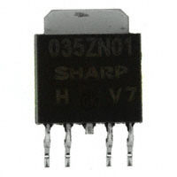
Lead finish identification mark
6.6MAX. 5.2±0.5
3
2.1±0.5
(0.3)
035ZN01
9.7MAX. 2.5MIN. 5.5±0.5 0.7 MAX.
Epoxy resin
H
(0~0.25) 0.3 +0.2 -0.1 (0.3)
Applications
1.AV equipment 2.OA equipment
1 2 4 5
4-(1.27)
(
) : Typical dimensions
Product mass:(0.2g)
1
Specific IC
3
Absolute Maximum Ratings
(Ta=25°C) Parameter *1 Input voltage *1 Bias supply voltage Symbol VIN VB *1 Vadj Output adjustment terminal voltage IO Output current *2 PD Power dissipation *3 Tj Junction temperature Topr Operating temperature Tstg Storage temperature Soldering temperature Tsol Rating Unit 5.5 V 7 V 5 V A 1 8 W 150 °C °C -40 to +85 -40 to +150 °C 260(10s) °C
1
2
4 5
2 3 4 5
DC input (VIN) Bias power supply (VB) DC output (VO) Output voltage adjustment (Vadj) GND
Lead finish:Lead-free solder plating (Composition: Sn2Cu)
*1 All are open except GND and applicable terminals. *2 PD:With infinite heat sink *3 There is case that over heat protection function operates at the temperature Tj=125°C to 150°C,this item cannot be used in this temperature range.
Notice The content of data sheet is subject to change without prior notice. In the absence of confirmation by device specification sheets, SHARP takes no responsibility for any defects that may occur in equipment using any SHARP devices shown in catalogs, data books, etc. Contact SHARP in order to obtain the latest device specification sheets before using any SHARP device.
1
Sheet No.: OP07008
(0.9)
(1.7)
�PQ035ZN01ZPH Electrical Characteristics
Parameter Input voltage Bias supply voltage Output voltage Load regulation Line regulation Reference voltage Temperature coefficient of reference voltage Ripple rejection Bias power supply input current
Unless otherwise specified,condition shall be VIN=1.8V,VB=3.3V,VO=1.2V(R1=1kΩ),IO=0.5A,Ta=25°C
Symbol VIN VB VO RegL RegI Vref TCVref RR1 RR2 IB
Conditions
MIN. 1.7
TYP.
MAX. 5.5
Unit V V V V % % V % dB dB mA
0.8V≤VO≤1.2V 1.2V<VO≤3.5V
VO+0.5
2.35 0.8
IO=5mA to 1A
VIN=1.7V to 5.5V,VB=2.35 to 7V , IO=5mA
Tj=0 to +125°C, IO=5mA Refer to Fig.2 Refer to Fig.3 IO=0A
0.57
0.2 0.3 0.6 ±0.5 65 53 1.5
5.5
7.0 3.5 0.5 0.7 0.63
-
2
Fig.1 Test Circuit
1
3 R2 A
VO
VB VIN 1μF A IB 1μF
IO
2 5
4
Vref 10μF R1 1kΩ V RL V
VO=Vref × (1+R2/R1) [R1=1kΩ, Vref≒ 0.6V]
Fig.2 Test Circuit for Ripple Rejection (1)
+
1
ei
3 R2
~
VB 2 5 1μF 1μF 4
IO
V ~ eo
Vref 10μF R1 1kΩ RL
VIN 1.8V
3.3V
f=120Hz(sine wave) ei(rms)=0.1V VIN=1.8V VB=3.3V VO=1.2V(R1=1kΩ) IO=0.3A RR=20log(ei(rms)/eo(rms))
Sheet No.: OP07008
2
�PQ035ZN01ZPH
Fig.3 Test Circuit for Ripple Rejection (2)
+
1
3 R2
VB
VIN 1.8V eb
IO
V ~ eo
2 5
4
Vref 10μF
1μF
~
3.3V
1μF
R1 1kΩ
RL
f=120Hz(sine wave) eb(rms)=0.1V VIN=1.8V VB=3.3V VO=1.2V(R1=1kΩ) IO=0.3A RR=20log(eb(rms)/eo(rms))
Fig.4 Power Dissipation vs. Ambient Temperature
10
Fig.5 Overcurrent Protection Characteristics
Power dissipation PD (mW)
PD:With infinite heat sink
Output voltage VO (V)
1.2 1.0 0.8 0.6 0.4 0.2
VIN=1.8V
8
VIN=2.5V VIN=3.3V VIN=5V
5
0 -40 -20
0
25
50
75 85 100 125 150
0 0
VB=3.3V CIN=1μF CO=10μF R1=R2=1kΩ Ta=Room temp.
0.5
1.0
1.5
2.0
2.5
3.0
Ambient temperature Ta (°C) Note) Oblique line portion:Overheat protection may operate in this area.
Output current IO (A)
Fig.6
0.602
Reference Voltage vs. Ambient Temperature
Fig.7 Load Regulation vs. Ambient Temperature
0.2
Rererance voltage Vref (V)
0.600 0.599 0.598 0.597 0.596 0.595
Load regulation RegL(%)
0.601
0 -0.2 -0.4 -0.6 -0.8 -1 -50 -25
VIN=1.8V VB=3.3V IO=0.5A CIN=1μF CO=10μF R1=R2=1kΩ
VIN=1.8V VB=3.3V IO=5mA~1A CIN=1μF CO=10μF R1=R2=1kΩ
-50 -25
0
25
50
75 100 125 150
0
25
50
75 100 125 150
Ambient temperature Ta (°C)
Ambient temperature Ta (°C)
Sheet No.: OP07008
3
�PQ035ZN01ZPH
Fig.8 Line Regulation vs. Ambient Temperature
0.7
Fig.9 Bias Inflow Current vs. Ambient Temperature
1
Line regulation RegI (%)
0.6 0.5 0.4 0.3 0.2 0.1 0 -50 -25 0 25 50
VIN=1.7~5.5V VB=2.35~7V IO=5mA CIN=1μF CO=10μF R1=R2=1kΩ
Bias inflow current IB (mA)
0.95
VIN=1.8V VB=3.3V IO=0A CIN=1μF CO=10μF R1=R2=1kΩ
0.9
0.85
0.8 0.75 -50 -25
75 100 125 150
0
25
50
75 100 125 150
Ambient temperature Ta (°C)
Ambient temperature Ta (°C)
Fig.10 Short circuit Current vs. Ambient Temperature
2.5 2.4
VIN=1.8V VB=3.3V RL=Short CIN=1μF CO=10μF
Fig.11 Output Voltage vs. Input Voltage
1.3 1.2
Short circuit current IS (A)
Output voltage VO (V)
2.3 2.2 2.1 2 1.9 1.8 1.7 1.6 1.5 -50 -25 0 25 50
1.0 0.8 0.6 0.4 0.2 0 0 1.0
IO=0A
IO=0.5A(RL=2.4Ω) IO=1A(RL=1.2Ω)
VB=3.3V CIN=1μF CO=10μF R1=R2=1kΩ Ta=Room temp.
75 100 125 150
2.0
3.0
4.0
Ambient temperature Ta (°C)
Input voltage VIN (V)
Fig.12 Output Voltage vs. Bias Supply Voltage
1.3 1.2
Fig.13 Dropout Voltage vs. Ambient Temperature
0.17 0.16
Output voltage VO (V)
1.0 0.8
IO=0A IO=0.5A(RL=2.4Ω) IO=1A(RL=1.2Ω)
Dropout voltage VI-O(V)
0.15 0.14 0.13 0.12 0.11 0.1 -50 -25 0 25 50
VIN=1.14V VB=3.3V IO=0.5A CIN=1μF CO=10μF R1=R2=1kΩ
0.6 0.4 0.2 0
VIN=1.8V CIN=1μF CO=10μF R1=R2=1kΩ Ta=Room temp.
0
1.0
2.0
3.0
4.0 4.5
75 100 125 150
Bias supply voltage VB (V)
Ambient temperature Ta (°C)
Sheet No.: OP07008
4
�PQ035ZN01ZPH
Fig.14 Output Voltage Deviation vs. Output Current
Output voltage deviation ΔVO (mV)
2.0 1.5 1.0 0.5 0 -0.5 -1.0 -1.5 -2.0 0 0.2 0.4 0.6 0.8 1.0
Fig.15 Output Voltage Deviation vs. Input Voltage / Bias Supply Voltage
Output voltage deviation ΔVO (mV)
2.5 2.0 1.5 1.0 0.5 0 -0.5 -1.0 -1.5 -2.0 -2.5 -3.0 0 1.0 2.0 3.0 4.0 5.0 6.0 7.0
VIN=1.8V VB=3.3V R1=R2=1kΩ IO=0A CIN=1μF CO=10μF
VB
VIN
Output current IO (A)
Input voltage / Bias supply voltage VIN/VB (V)
Fig.16 Input Current vs. Input Voltage
26 24 22 20 18 16 14 12 10 8 6 4 2 0 0 0.5 1.0 1.5 2.0 2.5 3.0 3.5 4.0
IO=0A VB=3.3V
Fig.17 Bias Inflow Current vs. Input Voltage
2.5
VB=3.3V
Bias inflow current IB (mA)
Input current IIN (mA)
2.0
IO=1A(RL=1.2Ω)
1.5
IO=0.5A(RL=2.4Ω)
1.0
IO=0A
0.5 0
0
0.5 1.0
1.5
2.0
2.5 3.0
3.5 4.0
Input voltage VIN (V)
Input voltage VIN (V)
Fig.18 Bias Inflow Current vs. Bias Supply Voltage
2.0
VIN=1.8V
IO=1A(RL=1.2Ω)
Fig.19 Output Voltage Adjustment Characteristics(Typical Value)
3.5 3.4 3.2 3 2.8 2.6 2.4 2.2 2 1.8 1.6 1.4 1.2 1 0.8 0.6 0.4 0.2 0
R1=1kΩ
Bias inflow current IB (mA)
1.5
IO=0.5A(RL=2.4Ω)
1.0 IB 0.5
IO=0A
0 0
Output voltage VO(V)
0.5 1.0
1.5
2.0 2.5 3.0
3.5 4.0
0
1000
2000
3000
4000
5000
Bias supply voltage VB (V)
R2(Ω)
Sheet No.: OP07008
5
�PQ035ZN01ZPH
Fig.20 Power Dissipation vs. Ambient Temperature (Typical Value)
Cu area 740mm2
Power dissipation PD (W)
2.0
Cu area 180mm2 Cu area 100mm2 Cu area 70mm2
Mounting PCB PCB Cu
1.5
1
Cu area 36mm2
0.5
Material : Glass-cloth epoxy resin Size : 50×50×1.6mm Cu thickness : 35μm
0 -40
-20
0
20
40
60 80
100 120
Ambient temperature Ta (°C)
Sheet No.: OP07008
6
�
很抱歉,暂时无法提供与“PQ035ZN01ZPH”相匹配的价格&库存,您可以联系我们找货
免费人工找货