PQ05VY3H3Z/PQ05VY053Z
PQ05VY3H3Z/ PQ05VY053Z
s Features
1. Low power-loss (Dropout voltage:MAX.0.5V) 2. Surface mount type (10.6×13.7×3.5mm) 3. Large output current 4. Low voltage operation (minimum operating voltage:2.35V) 5. High-preision output type (Reference voltage precision:±1.0%) 6. Overcurrent, overheat protection functions
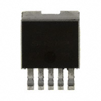
Surface Mount, Large Output Current Type Low Power-Loss Voltage Regulator
s Outline Dimensions
10.6MAX. (0.55) 3.28±0.5
6
(Unit : mm)
3.5±0.5 (0.6)
13.7MAX.
8.4±0.5
05VY3H3
(Heat sink is common to terminal 2 ) φ2
Epoxy resin (0.6) (0.45) +0.2 1.05−0.1 4−(1.7)
(2.4) 0 to 0.25 (0.6) (1.3)
(0.6) (0.45) +0.2 1.05−0.1
+0.2 3−0.9−0.1
s Applications
1. Peripheral equipment of personal computers 2. Power supplies for various electronic equipment such as AV or OA equipment
12345
s Model Line-up
Output current (IO) 3.5A 5A Package type Taping Sleeve Taping Sleeve Variable output PQ05VY3H3ZP PQ05VY3H3ZZ PQ05VY053ZP PQ05VY053ZZ
1 2 1 2
Specific IC
5 3 4
s Absolute Maximum Ratings
Parameter Symbol Rating Input voltage VIN 7 VI-O 4 Extremes of input-output voltage *1 VC Output control voltage 7 *1 VADJ 5 Output adjustment terminal voltage 3.5 PQ05VY3H3Z IO Output current 5 PQ05VY053Z *2 Power dissipation 35 PD *3 Junction temperature Tj 150 Topr Operating temperature −20 to +80 Storage temperature Tstg −40 to +150 Tsol Soldering temperature 260 (10s)
(Ta=25°C) Unit V V V V A W ˚C ˚C ˚C ˚C
3 4 5 6
DC input (VIN) DC output (VO) GND Output voltage adjustment (VADJ) ON/OFF control (VC) DC output (VO) ) : Typical dimensions
❈(
*1 All are open except GND and applicable terminals *2 PD:With infinite heat sink *3 Overheat protection may operate at the condition Tj=125˚C to 150˚C
Notice
In the absence of confirmation by device specification sheets, SHARP takes no responsibility for any defects that may occur in equipment using any SHARP devices shown in catalogs, data books, etc. Contact SHARP in order to obtain the latest device specification sheets before using any SHARP device. Internet Internet address for Electronic Components Group http://www.sharp.co.jp/ecg/
�PQ05VY3H3Z/PQ05VY053Z s Electrical Characteristics
Parameter
(Unless otherwise specified, condition shall be VIN=5V, IO=1.75A(PQ05VY3H3Z), IO=2.5A(PQ05VY053Z), VO=3V(R1=2kΩ), Ta=25˚C) MIN. TYP. MAX. Unit Symbol Conditions
VIN
Input voltage Output voltage Reference voltage Load regulation Line regulation Reference voltage fluctuation Ripple Rejection Dropout voltage
*5
VO Vref PQ05VY3H3Z PQ05VY053Z RegL RegI TCVref RR PQ05VY3H3Z PQ05VY053Z VI-O VC (ON) IC (ON) VC (OFF) IC (OFF) Iq
Output on control voltage Output on control current Output off control voltage Output off control current Quiescent current
− − − IO=5mA to 3.5A IO=5mA to 5A VIN=4 to 7V, IO=5mA Tj=0 to 125˚C, IO=5mA Refer to Fig.2 *4 IO=3.5A *4 IO=5A − VC=2.7V − VC=0.4V IO=0A
2.35 1.5 1.2276
− − 1.24 0.1 0.05 ±1 70 − − − − − 5
7 5
1.2524 0.5 0.1 − − 0.5 − 20 0.8 −0.4 10
V V V % % % dB V V µA V mA mA
− − − 60 − 2 − − − −
*4 The values of input voltage when output voltage goes 0.95V *5 In case of opening control terminal 5 , output voltage turns on
Fig.1 Standard Test Circuit
VIN 1 2 R2 + 100µF (Electrolytic capacitor) VC 5 4 A IC 3 A Iq R1 2kΩ V Vref + 100µF (Electrolytic capacitor) V RL VO
A
IO
VO=Vref×(1+R2/R1) . 1.24×(1+R /R ) =. 21 = = [R1. .2kΩ,Vref. .1.24V]
Fig.2 Test Circuit for Ripple Rejection
+ 1 ei ~ + 100µF (Electrolytic capacitor) 2.7V VC 5 4 2 R2 3 Vref + 100µF (Electrolytic capacitor) IO eo V ~ RL VO
VIN
R1 2kΩ
f=120Hz(sine wave) ei(rms)=0.5V VO=3V (R1=2kΩ) VIN=5V IO=0.5A RR=20log (ei(rms)/eo(rms))
�PQ05VY3H3Z/PQ05VY053Z Fig.3 Power Dissipation vs. Ambient Temperature
40 35 Power dissipation PD (W) 30 25 20 15 10 5 0 −25 0 25 50 75 100 PD : With infinite heat sink
Ambient temperature Ta (°C)
Note) Oblique line prtion:Overheat protection may operate in this area
Fig.4 Overcurrent Protection Characteristics (PQ05VY3H3Z)
100 VIO=3.7V VIO=1.7V Relative output voltage (%) VIO=1V VIO=0.5V 60
Fig.5 Overcurrent Protection Characteristics (PQ05VY053Z)
100 VIO=3.7V Relative output voltage (%) 80 VIO=1.7V VIO=1V 60 VIO=0.5V
80
40
40
20
20
0 0 1 2 3 4 5 6 7 8 9 10 11 12 Output current IO (A)
0 0 1 2 3 4 5 6 7 8 9 10 11 12 Output current IO (A)
Fig.6 Reference Voltage Fluctuation vs. Ambient Temperature
10 Reference voltage fluctuation ∆Vref (mV) 8 6 4 2 0 −2 −4 −6 −8 −10 −25 0 25 50 75 100 125 PQ05VY053Z VIN=5V IO=0 VO=3V
PQ05VY3H3Z
Ambient temperature Ta (°C)
�PQ05VY3H3Z/PQ05VY053Z Fig.7 Output Voltage vs. Input Voltage (PQ05VY3H3Z)
4 R1=2kΩ R2=2.8kΩ
Fig.8 Output Voltage vs. Input Voltage (PQ05VY053Z)
4 R1=2kΩ R2=2.8kΩ
Output voltage VO (V)
Output voltage VO (V)
3 RL=1.7Ω RL=∞Ω 2 RL=0.8Ω
3 RL=1.2Ω RL=∞Ω 2 RL=0.6Ω
1
1
0 0 1 2 3 4 5 6 7 Input voltage VIN (V)
0 0 1 2 3 4 5 6 7 Input voltage VIN (V)
Fig.9 Circuit Operating Current vs. Input Voltage (PQ05VY3H3Z)
160 Circuit operating current IBIAS (mA) 140 120 100 80 60 40 20 0 0 1 2 3 4 5 6 7 Input voltage VIN (V) RL=0.8Ω RL=1.7Ω RL=∞Ω R1=2kΩ R2=2.8kΩ (VO=3V)
Fig.10 Circuit Operating Current vs. Input Voltage (PQ05VY053Z)
160 Circuit operating current IBIAS (mA) 140 120 100 80 60 40 20 0 0 1 2 3 4 5 6 7 Input voltage VIN (V) RL=0.6Ω RL=1.2Ω RL=∞Ω R1=2kΩ R2=2.8kΩ (VO=3V)
Fig.11 Dropout Voltage vs. Junction Temperature
0.5 0.45 0.4 Dropout Voltage VI-O (V) 0.35 0.3 0.25 0.2 0.15 0.1 0.05 0 −40 −20 0 20 40 60 80 100 120 140 PQ05VY3H3Z:IO=3.5A PQ05VY053Z:IO=5A VIN=5V VO=3V
Fig.12 Quiescent Current vs. Junctiion Temperature
5 4.5 4 Quiescent current Iq (mA) 3.5 3 2.5 2 PQ05VY053Z 1.5 1 0.5 0 −40 −20 0 20 40 60 80 100 120 140 PQ05VY3H3Z VIN=5V IO=0A VO=3V VC=2V
Junction temperature Tj (°C)
Junction temperature Tj (°C)
�PQ05VY3H3Z/PQ05VY053Z Fig.13 ON-OFF Threshold Voltage vs. Junction Temperature
2 1.8 ON/OFF threshold voltage (V) 1.6 1.4 1.2 1 0.8 0.6 0.4 0.2 0 −40 −20 0 20 40 60 80 100 120 140 10 0 0.1 1 10 PQ05VY3H3Z PQ05VY053Z VIN=5V IO=0A VO=3V Ripple rejection RR (dB)
Fig.14 Ripple Rejection vs. Input Ripple Frequency
80 PQ05VY3H3Z 70 60 50 40 30 20 ei(rms)=0.5V VOUT=3V VIN=5V IO=0.5A COUT=100µF CIN=0 100 1 000 PQ05VY053Z
Junction temperature Tj (°C)
Input ripple frequency f (kHz)
Fig.15 Power Dissipation vs. Ambient Temperature (Typical Value)
6
5 Cu area 3 600mm2 Power dissipation PD (W) 4 Cu area 900mm2 Cu area 400mm2 Cu area 115mm
2
3
PWB PWB Cu
2 1 0 −20
Material : Glass-cloth epoxy resin Size : 60×60×1.6mm Cu thickness : 65µm 0 20 40 60 80 Ambient temperature Ta (°C)
Fig.16 Output Voltage Adjustment Characteristics (Typical Value)
5 4.5 4 Output voltage VO (V) 3.5 3 2.5 2 1.5 1 0.5 0 100 1 000 R2 (Ω) 10 000 R1=2kΩ
�PQ05VY3H3Z/PQ05VY053Z Fig.17 Example of Application
DC input 1 2 R2 VIN CIN 5 3 4 R1 2kΩ CO + Load VO
ON/OFF control signal
High:Output ON Low:Output OFF Open:Outout ON (Note)
❈ Please make sure to use this device, pulling up to the power supply with less than 7V at the resistor less than 50kΩ in switching ON/OFF with open collector output or in not using ON/OFF function (in keeping "ON"), because input impedance is high in ON/OFF terminals.
�PQ05VY3H3Z/PQ05VY053Z s Precautions for Use
VIN 1 2 R2 CIN 5 3 4 R1 CO + Load VO
C-MOS or TTL
1. External connection (1) The connecting wiring of CO and each terminal must be as short as possible. Owing to type, value and wiring condition of capacitor, it may oscillate. Confirm the output waveform under the actual condition before using. (2) ON/OFF control terminal 5 is compatible with LS-TTL. It enables to be directly drive by TTL or C-MOS standard logic (RCA4000 series). Please make sure to use this device, pulling up to the power supply with less than 7V at the resistor less than 50kΩ in switching ON/OFF with open collector output or in not using ON/OFF function (in keeping "ON"), because input impedance is high in ON/OFF terminals. (3) If voltage is applied under the conditions that the device pin is connected divergently or reversely, the deterioration of characteristics or damage may occur. Never allow improper mounting. (4) If voltage exceeding the voltage of DC input terminal 1 is applied to the output terminal 2 , the element may be damaged. Especially when the DC input terminal 1 is short-circuited to the GND in ordinary operating state, charges accumulated in the output capacitor CO flow to the input side, causing damage to the element. In this case, connect the ordinary silicon diode as shown in the figure. 2. Thermal protection design Maximum power dissipation of devices is obtained by the following equation. PD=IO×(VIN−VO)+VIN×Iq When ambient temperature Ta and power dissipation PD (MAX.) during operation are determined, operate element within the safety operation area specified by the derating curve. Insufficient radiation gives an unfavorable influence to the normal operation and reliability of the device. In the external area of the safety operation area shown by the derating curve, the overheat protection circuit may operate to shutdown output. However please avoid keeping such condition for a long time. 3. ESD (Electrostatic Sensitivity Discharge) Be careful not to apply electrostatic discharge to the device since this device employs a bipolar IC and may be damaged by electro static discharge. Followings are some methods against excessive voltage caused by electro static discharge. (1) Human body must be grounded to discharge the electro charge which is charged in the body or cloth. (2) Anything that is in contact with the device such as workbench, inserter, or measuring instrument must be grounded. (3) Use a soldering dip basin with a minimum leak current (isolation resistance 10MΩ or more) from the AC power supply line. Also the soldering dip basin must be grounded.
1
2
�PQ05VY3H3Z/PQ05VY053Z s Output Voltage Fine Tuning
1. Connecting external resistors R1 and R2 to terminals 2 , 3 , 4 allows the output voltage to be fine tuned from 1.5V to 5V. Refer to Fig.16 when connecting external resistors for fine tuning output voltage.
2 R2 − + 3 Vref 4 R1
VO
VO=Vref×(1+R2/R1) . 1.24×(1+R /2 000) =. 2 [R1=2kΩ, Vref=1.24V]
�Application Circuits
NOTICE
qThe circuit application examples in this publication are provided to explain representative applications of SHARP devices and are not intended to guarantee any circuit design or license any intellectual property rights. SHARP takes no responsibility for any problems related to any intellectual property right of a third party resulting from the use of SHARP's devices. qContact SHARP in order to obtain the latest device specification sheets before using any SHARP device. SHARP reserves the right to make changes in the specifications, characteristics, data, materials, structure, and other contents described herein at any time without notice in order to improve design or reliability. Manufacturing locations are also subject to change without notice. qObserve the following points when using any devices in this publication. SHARP takes no responsibility for damage caused by improper use of the devices which does not meet the conditions and absolute maximum ratings to be used specified in the relevant specification sheet nor meet the following conditions: (i) The devices in this publication are designed for use in general electronic equipment designs such as: --- Personal computers --- Office automation equipment --- Telecommunication equipment [terminal] --- Test and measurement equipment --- Industrial control --- Audio visual equipment --- Consumer electronics (ii)Measures such as fail-safe function and redundant design should be taken to ensure reliability and safety when SHARP devices are used for or in connection with equipment that requires higher reliability such as: --- Transportation control and safety equipment (i.e., aircraft, trains, automobiles, etc.) --- Traffic signals --- Gas leakage sensor breakers --- Alarm equipment --- Various safety devices, etc. (iii)SHARP devices shall not be used for or in connection with equipment that requires an extremely high level of reliability and safety such as: --- Space applications --- Telecommunication equipment [trunk lines] --- Nuclear power control equipment --- Medical and other life support equipment (e.g., scuba). qContact a SHARP representative in advance when intending to use SHARP devices for any "specific" applications other than those recommended by SHARP or when it is unclear which category mentioned above controls the intended use. qIf the SHARP devices listed in this publication fall within the scope of strategic products described in the Foreign Exchange and Foreign Trade Control Law of Japan, it is necessary to obtain approval to export such SHARP devices. qThis publication is the proprietary product of SHARP and is copyrighted, with all rights reserved. Under the copyright laws, no part of this publication may be reproduced or transmitted in any form or by any means, electronic or mechanical, for any purpose, in whole or in part, without the express written permission of SHARP. Express written permission is also required before any use of this publication may be made by a third party. qContact and consult with a SHARP representative if there are any questions about the contents of this publication.
115
�