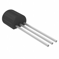
BS 170
SIPMOS ® Small-Signal Transistor • N channel • Enhancement mode • Logic Level
• VGS(th) = 0.8...2.0V
Pin 1 S Type BS 170 Type BS 170
Pin 2 G Marking BS 170
Pin 3 D
VDS
60 V
ID
0.3 A
RDS(on)
5Ω
Package TO-92
Ordering Code Q67000-S076
Tape and Reel Information E6288
Maximum Ratings Parameter Drain source voltage Drain-gate voltage Symbol Values 60 60 Unit V
VDS V
DGR
RGS = 20 kΩ
Gate source voltage Gate-source peak voltage,aperiodic Continuous drain current
VGS Vgs ID
± 14 ± 20 A 0.3
TA = 25 °C
DC drain current, pulsed
IDpuls
1.2
TA = 25 °C
Power dissipation
Ptot
0.63
W
TA = 25 °C
Semiconductor Group
1
12/05/1997
�BS 170
Maximum Ratings Parameter Chip or operating temperature Storage temperature Thermal resistance, chip to ambient air 1) DIN humidity category, DIN 40 040 IEC climatic category, DIN IEC 68-1 Symbol Values -55 ... + 150 -55 ... + 150 ≤ 200 E 55 / 150 / 56 K/W Unit °C
Tj Tstg RthJA
Electrical Characteristics, at Tj = 25°C, unless otherwise specified Parameter Symbol min. Static Characteristics Drain- source breakdown voltage Values typ. max. Unit
V(BR)DSS
60 1.4 0.05 1 2.5 2
V
VGS = 0 V, ID = 0.25 mA, Tj = 25 °C
Gate threshold voltage
VGS(th)
0.8
VGS=VDS, ID = 1 mA
Zero gate voltage drain current
IDSS
0.5 5
µA
VDS = 60 V, VGS = 0 V, Tj = 25 °C VDS = 60 V, VGS = 0 V, Tj = 125 °C
Gate-source leakage current
IGSS
10
nA Ω 5
VGS = 20 V, VDS = 0 V
Drain-Source on-state resistance
RDS(on)
VGS = 10 V, ID = 0.2 A
Semiconductor Group
2
12/05/1997
�BS 170
Electrical Characteristics, at Tj = 25°C, unless otherwise specified Parameter Symbol min. Dynamic Characteristics Transconductance Values typ. max. Unit
gfs
0.12 0.18 40 15 5 -
S pF 60 25 10 ns 5 8
VDS≥ 2 * ID * RDS(on)max, ID = 0.2 A
Input capacitance
Ciss Coss
-
VGS = 0 V, VDS = 25 V, f = 1 MHz
Output capacitance
VGS = 0 V, VDS = 25 V, f = 1 MHz
Reverse transfer capacitance
Crss
-
VGS = 0 V, VDS = 25 V, f = 1 MHz
Turn-on delay time
td(on)
VDD = 30 V, VGS = 10 V, ID = 0.29 A RG = 50 Ω
Rise time
tr
8 12
VDD = 30 V, VGS = 10 V, ID = 0.29 A RG = 50 Ω
Turn-off delay time
td(off)
12 16
VDD = 30 V, VGS = 10 V, ID = 0.29 A RG = 50 Ω
Fall time
tf
17 22
VDD = 30 V, VGS = 10 V, ID = 0.29 A RG = 50 Ω
Semiconductor Group
3
12/05/1997
�BS 170
Electrical Characteristics, at Tj = 25°C, unless otherwise specified Parameter Symbol min. Reverse Diode Inverse diode continuous forward current IS A 0.9 0.3 1.2 V 1.2 Values typ. max. Unit
TA = 25 °C
Inverse diode direct current,pulsed
ISM
-
TA = 25 °C
Inverse diode forward voltage
VSD
VGS = 0 V, IF = 0.5 A
Semiconductor Group
4
12/05/1997
�BS 170
Power dissipation Ptot = ƒ(TA)
Drain current ID = ƒ(TA) parameter: VGS ≥ 10 V
0.32
0.70 W 0.60
A
Ptot
0.55 0.50 0.45 0.40 0.35 0.30 0.25 0.20
ID
0.24
0.20
0.16
0.12
0.08 0.15 0.10 0.05 0.00 0 0.04 0.00 0
20
40
60
80
100
120
°C
160
20
40
60
80
100
120
°C
160
TA
TA
Safe operating area ID=f(VDS) parameter : D = 0.01, TC=25°C
Drain-source breakdown voltage V(BR)DSS = ƒ(Tj)
71 V 68
V(BR)DSS
66 64
62
60
58
56 54 -60
-20
20
60
100
°C
160
Tj
Semiconductor Group
5
12/05/1997
�BS 170
Typ. output characteristics ID = ƒ(VDS) parameter: tp = 80 µs , Tj = 25 °C
0.70 A 0.60
Typ. drain-source on-resistance RDS (on) = ƒ(ID) parameter: tp = 80 µs, Tj = 25 °C
16
Ptot = 1W
lkj i h
VGS [V] a 2.0
b 2.5 3.0 3.5 4.0 4.5 5.0 6.0 7.0 8.0 9.0 10.0
Ω
g
a
b
c
d
e
ID
0.55 0.50 0.45 0.40 0.35 0.30 0.25 0.20 0.15
RDS (on)
12
c d
10
f
e f g
8
e
h i j
6
dk
l
4 2 VGS [V] =
a 2.5 2.0 3.0 b 3.5 c 4.0 d 4.5 e f 5.0 6.0 g 7.0 h i j 8.0 9.0 10.0
c
f hj ig
0.10 0.05 b a 0.00 0.0 0.5 1.0 1.5 2.0 2.5 3.0 3.5 4.0
V
5.0
0 0.00
0.10
0.20
0.30
0.40
A
0.60
VDS
ID
Typ. transfer characteristics ID = f(VGS) parameter: tp = 80 µs VDS≥ 2 x ID x RDS(on)max
0.75 A 0.65
Typ. forward transconductance gfs = f (ID) parameter: tp = 80 µs, VDS≥2 x ID x RDS(on)max
0.30 S 0.26
ID
0.60 0.55 0.50 0.45 0.40 0.35 0.30 0.25 0.20 0.15 0.10 0.05 0.00 0
gfs
0.24 0.22 0.20 0.18 0.16 0.14 0.12 0.10 0.08 0.06 0.04 0.02 0.00 0.00
1
2
3
4
5
6
7
8
V VGS
10
0.10
0.20
0.30
0.40
0.50
A ID
0.65
Semiconductor Group
6
12/05/1997
�BS 170
Drain-source on-resistance RDS (on) = ƒ(Tj) parameter: ID = 0.2 A, VGS = 10 V
13
Gate threshold voltage VGS (th) = ƒ(Tj) parameter: VGS = VDS, ID = 1 mA
4.6 V 4.0
Ω
11
RDS (on)
10 9 8 7
VGS(th)
3.6 3.2 2.8
98%
6 5
2.4
98%
2.0 1.6
typ
4 3 2 1 0 -60 -20 20 60 100 °C 160
typ
1.2
2%
0.8 0.4 0.0 -60 -20 20 60 100 °C 160
Tj
Tj
Typ. capacitances C = f (VDS) parameter:VGS=0V, f = 1 MHz
10 3
Forward characteristics of reverse diode IF = ƒ(VSD) parameter: Tj, tp = 80 µs
10 1
pF C 10 2
A
IF
10 0
Ciss
10 1
Coss
10 - 1
Tj = 25 °C typ Crss Tj = 150 °C typ Tj = 25 °C (98%) Tj = 150 °C (98%)
10 0 0 10 -2 0.0
5
10
15
20
25
30
V VDS
40
0.4
0.8
1.2
1.6
2.0
2.4
V
3.0
VSD
Semiconductor Group
7
12/05/1997
�
很抱歉,暂时无法提供与“BS170”相匹配的价格&库存,您可以联系我们找货
免费人工找货