Rev.1.2_00
TEMPERATURE SWITCH IC WITH LATCH
S-5840B Series
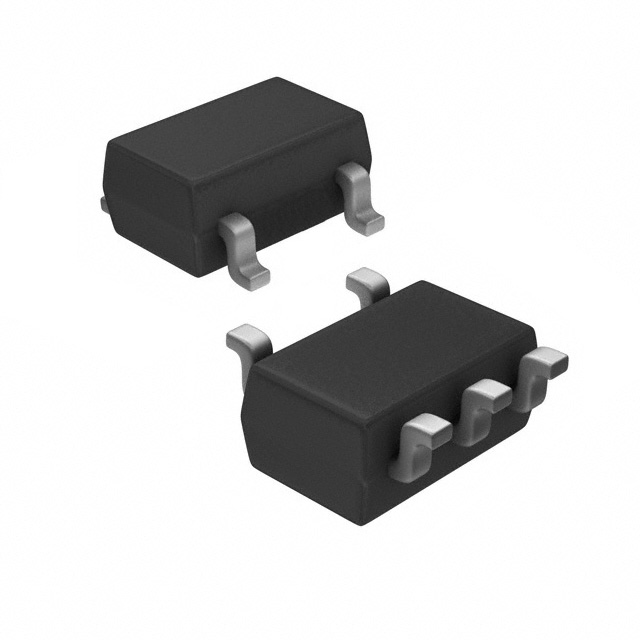
The temperature switch IC S-5840B Series with a latch function detects temperature with the accuracy of ±2.5°C. When the temperature reaches the detection temperature, the output signal is inverted and being latched until this IC detects decrease in a power supply voltage. The minimum power supply voltage is 1.0 V which is required to operate this IC, the current consumption is as low as 12 µA (typ.) due to CMOS configuration. The S-5840B Series has a temperature sensor using negative temperature coefficient, a reference voltage source, comparator, voltage detection circuit and noise suppression circuit on a chip, and they are enclosed in package SOT-23-5. Since the temperature range of this IC is −40 to +100°C, it is possible to achieve the extensive application for temperature control.
Features
• • • • • • • • • • Detection temperature : +55 to +95°C, 1°C step, detection accuracy : ±2.5°C Wide voltage range during operation : VDD = 1.0 to 10.0 V Release voltage : 2.2 to 3.4 V, 0.1 V step Low current consumption : 12 µA typ. (+25°C) Built-in circuit for preventing temperature detection malfunction Output logic level is fixed by the latch after temperature detection Output logic active high or active low is selectable Output CMOS or Nch open drain is selectable Package : SOT-23-5 Lead-free product
Applications
• Game consoles • Electronic devices
Package
Package Name SOT-23-5 Package MP005-A Drawing Code Tape MP005-A Reel MP005-A
Seiko Instruments Inc.
1
�TEMPERATURE SWITCH IC WITH LATCH S-5840B Series Block Diagram
1. S-5840B with CMOS output
VDD
Rev.1.2_00
Temperature Sensor
+ VREF CD
Reference Voltage Source Voltage Detector
DQ D-F/F CK R
DET
VSS
RT
Figure 1 2. S-5840B with Nch open drain output
VDD
Temperature Sensor
+ VREF CD
Reference Voltage Source Voltage Detector
DQ D-F/F CK R
DET
VSS
RT
Figure 2
2
Seiko Instruments Inc.
�Rev.1.2_00 Product Name Structure
1. Product name
S-5840B xx - M5T1 G
TEMPERATURE SWITCH IC WITH LATCH S-5840B Series
Package abbreviation and IC packing specifications*1 M5T1 : SOT-23-5, tape Option code*2
*1. Refer to the taping specifications at the end of this booklet. *2. Option list • Detection temperature (TDET) is selectable in 1°C step in the range of 55 to 95°C. • DET output is selectable in active high or active low. • DET output is selectable in CMOS or Nch open drain. • Release voltage (VRET) is selectable in 0.1 V step in the range of 2.2 to 3.4 V.
2. Product name list
Table 1
Output form Output logic Detection temperature (TDET) S-5840BAG-M5T1G 60°C CMOS Active low S-5840BAH-M5T1G 90°C CMOS Active high S-5840BAJ-M5T1G 80°C Nch open drain Active low Remark Please contact our sales office for options other than that specified above. Product name
Release voltage (VRET) 2.9 V 2.9 V 2.2 V
Seiko Instruments Inc.
3
�TEMPERATURE SWITCH IC WITH LATCH S-5840B Series Pin Configuration
SOT-23-5 Top view 5 4
Table 2
Rev.1.2_00
Pin No. 1 2 3
Symbol RT *1 VSS CD
1
2
Figure 3
3
*1.
4 DET 5 VDD Set the RT pin open in use.
Description Test pin GND pin Capacitor connection pin for setting malfunction prevention time Output pin Power supply pin
Remark See Dimensions for details of the package drawings.
Absolute Maximum Ratings
Table 3
Parameter Power supply voltage (VSS = 0 V) Pin voltage Output voltage Power dissipation Operating temperature Storage temperature CMOS output Nch open drain output
Symbol VDD VRT, VCD VDET PD Topr Tstg
(Ta = 25°C unless otherwise specified) Rating Unit VSS + 12 V VSS − 0.3 to VDD + 0.3 VSS − 0.3 to VDD + 0.3 VSS − 0.3 to VSS + 12.0 300 (When not mounted on board) 600*1
−40 to +100 −55 to +125
V V V mW mW
°C °C
*1. When mounted on board [Mounted board] (1) Board size : 114.3 mm × 76.2 mm × t1.6 mm (2) Board name : JEDEC STANDARD51-7 Caution The absolute maximum ratings are rated values exceeding which the product could suffer physical damage. These values must therefore not be exceeded under any conditions.
Recommended Values for External Parts
Table 4
Parameter CD capacitance
Symbol CD
Value 4.7
Unit nF
4
Seiko Instruments Inc.
�Rev.1.2_00 DC Electrical Characteristics
1. Product with CMOS output
TEMPERATURE SWITCH IC WITH LATCH S-5840B Series
Table 5 Parameter Power supply voltage Detection temperature Output current Release voltage for built-in voltage detector Hysteresis width for built-in voltage detector Temperature coefficient for built-in voltage detector Operating current Symbol VDD TD IDETH IDETL VR VHYS
∆VRET ∆Ta • VRET
Conditions − − VDD = 3.5 V, Apply for DET pin − − VDET = 2.7 V VDET = 0.4 V
(Ta = 25°C, unless otherwise specified) Min. Typ. Max. Unit 1.0 TDET − 2.5 2 0.5 VRET × 0.98 − − TDET 9.4 2.8 VRET VRET × 0.05 ±100 12 10.0 TDET + 2.5 − − VRET × 1.02 − V °C mA mA V V ppm/ °C µA
Ta = −40 to +100°C VDD = 3.5 V
− −
− 24
IDD
2. Product with Nch open drain output Table 6 Parameter Power supply voltage Detection temperature Output current Release voltage for built-in voltage detector Hysteresis width for built-in voltage detector Temperature coefficient for built-in voltage detector Operating current Symbol VDD TD IDETL ILEAK VR VHYS
∆VRET ∆Ta • VRET
Conditions − − VDET = 0.4 V, VDD = 3.5 V VDET = 10.0 V, VDD = 3.5 V − −
(Ta = 25°C, unless otherwise specified) Min. Typ. Max. Unit 1.0 − 10.0 V TDET − 2.5 TDET TDET + 2.5 °C 0.5 − VRET × 0.98 − 2.8 − VRET VRET × 0.05 ±100 12 − 100 VRET × 1.02 − mA nA V V ppm/ °C µA
Ta = −40 to +100°C VDD = 3.5 V
− −
− 24
IDD
AC Electrical Characteristics
Table 7 Parameter Noise filtering time Symbol tnoise Conditions CD = 4.7 nF, VDD = 3.5 V, Ta = detection temperature Min. 10 Typ. 30 Max. 50 Unit ms
Seiko Instruments Inc.
5
�TEMPERATURE SWITCH IC WITH LATCH S-5840B Series Operation
Basic operation
Rev.1.2_00
The S-5840B Series is a temperature switch IC which detects the temperature and sends a signal to an external device. The users can select a combination of the parameters such as detection temperature and release voltage. The following explains the case when DET output is assumed to be active high. When the power supply voltage is turned on, the DET pin voltage goes to low since the flip-flop circuit in the detection circuit is cleared by the voltage detection circuit. Temperature detection then starts and the DET pin is held low as long as the temperature is lower than the detection temperature. When the temperature rises and when the temperature exceeds the detection temperature; longer than the time defined by the capacitor connected to the CD pin, the DET pin goes to high. Once the over-temperature is detected and the DET pin goes to high, the state is held by the flip-flop circuit. In order to release the state, the power supply voltage should be set under the detection voltage (VR − VHYS) of the built-in voltage detector circuit to reset the internal circuit. Using the internal reference voltage and built-in temperature sensor, a detection temperature accuracy of ±2.5°C is achieved in the IC.
[Noise filtering circuit]
The noise filtering circuit prevents malfunction of the temperature switch caused by noise. The noise filtering circuit starts charging the capacitor connected to the CD pin when the output of the internal comparator enters the active state due to an external noise or a rapid change in the power supply voltage. In the normal operation, the flip-flop circuit is set when the capacitor is charged to a certain voltage. But in the noise triggered operation, the comparator output goes back to the inactive state and the CD pin voltage is held low since the charging of the capacitor is insufficient. As a result, the DET pin is held low and malfunction does not occur. Noise filtering time (tnoise) is determined by the time constant consisting of internal constant current and the capacitance (CD), and calculated by the following equation. tnoise (ms) = Noise filtering time coefficient × CD (nF) Noise filtering time coefficient (25°C) : Typ. 6.4 Capacitance of the external capacitor CD has no limitation as long as its leak current is negligible compared to the internal constant current. The difference occurs in delay time if the capacitor has a leak current.
6
Seiko Instruments Inc.
�Rev.1.2_00 Application Circuit
TEMPERATURE SWITCH IC WITH LATCH S-5840B Series
Open VDD RT
R 100 kΩ
*1
S-5840B Series
CIN CD CD
DET VSS
Protection Circuit
CL
*1.
Connecting a resistor (R) is unnecessary for the product with CMOS output.
Figure 4
Caution The above connection diagram will not guarantee successful operation. evaluation using actual application to set the constant.
Perform thorough
Precautions
• Set a capacitor (CIN) of about 0.1 µF between VDD and VSS for stabilization. • A capacitor (CL) of about 1 µF should be connected to the DET pin to prevent malfunction caused by noise due to the power being on. • Do not connect a capacitor to the RT pin (leave the RT pin open). Otherwise, this IC may oscillate. • Do not apply an electrostatic discharge to this IC that exceeds the performance ratings of the built-in electrostatic protection circuit. • SII claims no responsibility for any disputes arising out of or in connection with any infringement by products, including this IC, of patents owned by a third party.
Seiko Instruments Inc.
7
�TEMPERATURE SWITCH IC WITH LATCH S-5840B Series Characteristics (Typical Data)
1. Current consumption vs. Power supply voltage characteristics
Rev.1.2_00
13 12
IDD [µA]
VSS = 0 V −40°C 100°C
11 10 9
25°C
0 1 2 3 4 5 6 7 8 9 10 11 12 VDD [V]
2. DET pin current H vs. Power supply voltage characteristics (product with CMOS output)
VDET = VDD − 0.8 V 25°C
25 20
IDETH [mA]
15 10 5 0
−40°C
100°C
0 1 2 3 4 5 6 7 8 9 10 11 12 VDD [V]
3. DET pin current L vs. Power supply voltage characteristics
10 8
IDETL [mA]
VDET = 0.4 V 25°C −40°C
6 4 2 0
100°C 0 1 2 3 4 5 6 7 8 9 10 11 12 VDD [V]
4. Noise filtering time vs. Power supply voltage characteristics
CD = 4.7 nF −40°C 25°C 100°C 0 1 2 3 4 5 6 7 8 9 10 11 12 VDD [V]
50 45 40 35 30 25 20 15 10
tnoise [ms]
8
Seiko Instruments Inc.
�Rev.1.2_00 Marking Specification
SOT-23-5
SOT-23-5 Top view 5 4
TEMPERATURE SWITCH IC WITH LATCH S-5840B Series
(1) to (3) : (4) :
Product code (refer to Product name vs. Product code) Lot number
(1) (2) (3) (4)
1
2
3
Product name vs. Product code
Product Name S-5840BAG-M5T1G S-5840BAH-M5T1G S-5840BAJ-M5T1G
Product Code (1) (2) (3) H 8 M H 8 N H 8 O
Seiko Instruments Inc.
9
�2.9±0.2 1.9±0.2
5 4
1
2
3
0.16 -0.06
+0.1
0.95±0.1 0.4±0.1
No. MP005-A-P-SD-1.2
TITLE No. SCALE UNIT
SOT235-A-PKG Dimensions MP005-A-P-SD-1.2
mm
Seiko Instruments Inc.
�4.0±0.1(10 pitches:40.0±0.2)
+0.1
ø1.5 -0
2.0±0.05
0.25±0.1
ø1.0 -0
+0.2
4.0±0.1 1.4±0.2
3.2±0.2
321
4
5
Feed direction
No. MP005-A-C-SD-2.1
TITLE No. SCALE UNIT
SOT235-A-Carrier Tape MP005-A-C-SD-2.1
mm
Seiko Instruments Inc.
�12.5max.
Enlarged drawing in the central part ø13±0.2
9.0±0.3
(60°)
(60°)
No. MP005-A-R-SD-1.1
TITLE No. SCALE UNIT mm
SOT235-A-Reel MP005-A-R-SD-1.1
QTY. 3,000
Seiko Instruments Inc.
�• • • • • •
The information described herein is subject to change without notice. Seiko Instruments Inc. is not responsible for any problems caused by circuits or diagrams described herein whose related industrial properties, patents, or other rights belong to third parties. The application circuit examples explain typical applications of the products, and do not guarantee the success of any specific mass-production design. When the products described herein are regulated products subject to the Wassenaar Arrangement or other agreements, they may not be exported without authorization from the appropriate governmental authority. Use of the information described herein for other purposes and/or reproduction or copying without the express permission of Seiko Instruments Inc. is strictly prohibited. The products described herein cannot be used as part of any device or equipment affecting the human body, such as exercise equipment, medical equipment, security systems, gas equipment, or any apparatus installed in airplanes and other vehicles, without prior written permission of Seiko Instruments Inc. Although Seiko Instruments Inc. exerts the greatest possible effort to ensure high quality and reliability, the failure or malfunction of semiconductor products may occur. The user of these products should therefore give thorough consideration to safety design, including redundancy, fire-prevention measures, and malfunction prevention, to prevent any accidents, fires, or community damage that may ensue.
�