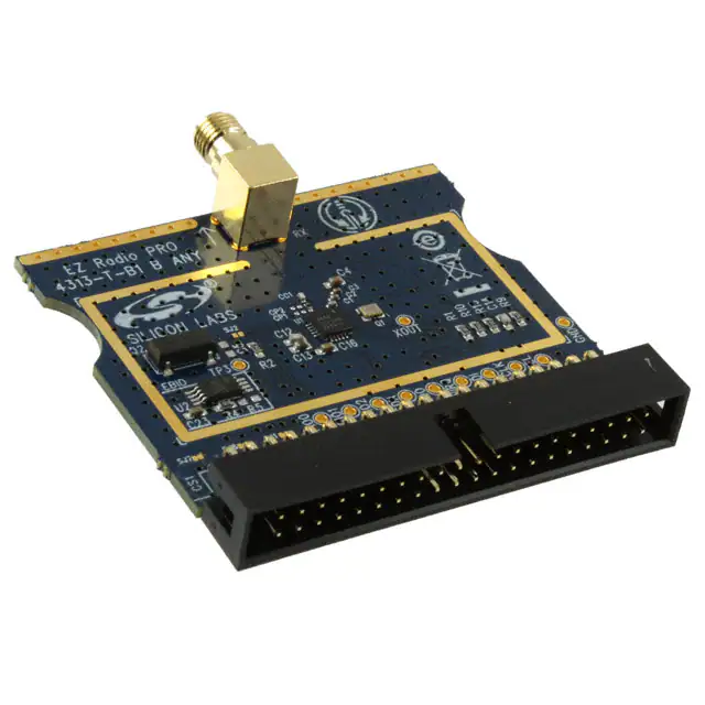
Si4313-B1
Si4313 L OW -C O S T I S M R ECEIVER
Features
Ordering Information:
See page 44.
Pin Assignments
Si4313
Applications
Personal data logging
Health monitors
VDD 1
20 19 18 17 16
NC 2
15 SCLK
NC 3
RX 4
12 VDD_DIG
6
7
8
9
GPIO_2
The Si4313 offers a simple, single-ended radio implementation over the
240–960 MHz frequency range. A receive sensitivity of up to –118 dBm
allows for the creation of communication links with an extended range.
The Si4313 offers excellent receiver performance in cost-sensitive radio
applications.
13 SDO
NC 5
GPIO_0
The Si4313 is a single-ended universal ISM receiver for cost-sensitive
applications featuring technology developed for the EZRadioPRO®
product family.
GPIO_1
Description
14 SDI
GND
PAD
NC
Remote control
Weather station
nSEL
nIRQ
10 11 NC
VDR
Programmable RX BW
2.6–620 kHz
Preamble detector
RX 64 byte FIFO
–40 to +85 °C temperature range
Integrated voltage regulators
Frequency hopping capability
On-chip crystal tuning
20-pin QFN package
Low BOM
Single capacitor matching network
Power-On-Reset (POR)
Single-ended antenna
configuration
XOUT
Frequency range = 240–960 MHz
Sensitivity = –118 dBm
Low power consumption
Data rate = 0.2 to 128 kbps
FSK, GFSK, and OOK modulation
schemes
Power supply = 1.8 to 3.6 V
Ultra low power shutdown mode
Digital RSSI
Wake-up timer
Auto frequency calibration (AFC)
Clear channel assessment
XIN
SDN
Patents pending
The Si4313 provides designers with advanced features to enable low
system power consumption by offloading a number of RF-related
activities from the system MCU allowing for extended MCU sleep periods.
Additional features, such as an automatic wake-up timer, 64-byte RX
FIFO, and a preamble detection circuit, are available.
The Si4313's digital receive architecture features an ADC and DSP based
modem that performs the radio demodulation and filtering for increased
performance.
Rev. 1.0 3/11
Copyright © 2011 by Silicon Laboratories
Si4313
�Si4313-B1
Functional Block Diagram
2
Rev. 1.0
�Si4313-B1
TABLE O F C ONTENTS
Section
Page
1. Electrical Specifications . . . . . . . . . . . . . . . . . . . . . . . . . . . . . . . . . . . . . . . . . . . . . . . . . . .7
1.1. Test Condition Definitions . . . . . . . . . . . . . . . . . . . . . . . . . . . . . . . . . . . . . . . . . . . . . 14
2. Functional Description . . . . . . . . . . . . . . . . . . . . . . . . . . . . . . . . . . . . . . . . . . . . . . . . . . . 15
2.1. Application Example . . . . . . . . . . . . . . . . . . . . . . . . . . . . . . . . . . . . . . . . . . . . . . . . . 15
2.2. Operating Modes . . . . . . . . . . . . . . . . . . . . . . . . . . . . . . . . . . . . . . . . . . . . . . . . . . . . 16
3. Controller Interface . . . . . . . . . . . . . . . . . . . . . . . . . . . . . . . . . . . . . . . . . . . . . . . . . . . . . . 17
3.1. Serial Peripheral Interface . . . . . . . . . . . . . . . . . . . . . . . . . . . . . . . . . . . . . . . . . . . . . 17
3.2. Operating Mode Control . . . . . . . . . . . . . . . . . . . . . . . . . . . . . . . . . . . . . . . . . . . . . . 19
3.3. Interrupts . . . . . . . . . . . . . . . . . . . . . . . . . . . . . . . . . . . . . . . . . . . . . . . . . . . . . . . . . . 21
3.4. System Timing . . . . . . . . . . . . . . . . . . . . . . . . . . . . . . . . . . . . . . . . . . . . . . . . . . . . . 22
3.5. Frequency Control . . . . . . . . . . . . . . . . . . . . . . . . . . . . . . . . . . . . . . . . . . . . . . . . . . . 22
4. Modulation Options . . . . . . . . . . . . . . . . . . . . . . . . . . . . . . . . . . . . . . . . . . . . . . . . . . . . . . 25
4.1. Modulation Type . . . . . . . . . . . . . . . . . . . . . . . . . . . . . . . . . . . . . . . . . . . . . . . . . . . .25
4.2. FIFO Mode . . . . . . . . . . . . . . . . . . . . . . . . . . . . . . . . . . . . . . . . . . . . . . . . . . . . . . . .25
4.3. Direct Mode . . . . . . . . . . . . . . . . . . . . . . . . . . . . . . . . . . . . . . . . . . . . . . . . . . . . . . . .25
5. Internal Functional Blocks . . . . . . . . . . . . . . . . . . . . . . . . . . . . . . . . . . . . . . . . . . . . . . . . 26
5.1. RX LNA . . . . . . . . . . . . . . . . . . . . . . . . . . . . . . . . . . . . . . . . . . . . . . . . . . . . . . . . . . . 26
5.2. RX I-Q Mixer . . . . . . . . . . . . . . . . . . . . . . . . . . . . . . . . . . . . . . . . . . . . . . . . . . . . . . .26
5.3. Programmable Gain Amplifier . . . . . . . . . . . . . . . . . . . . . . . . . . . . . . . . . . . . . . . . . .26
5.4. ADC . . . . . . . . . . . . . . . . . . . . . . . . . . . . . . . . . . . . . . . . . . . . . . . . . . . . . . . . . . . . . . 26
5.5. Digital Modem . . . . . . . . . . . . . . . . . . . . . . . . . . . . . . . . . . . . . . . . . . . . . . . . . . . . . . 26
5.6. Synthesizer . . . . . . . . . . . . . . . . . . . . . . . . . . . . . . . . . . . . . . . . . . . . . . . . . . . . . . . .27
5.7. Crystal Oscillator . . . . . . . . . . . . . . . . . . . . . . . . . . . . . . . . . . . . . . . . . . . . . . . . . . . .27
5.8. Regulators . . . . . . . . . . . . . . . . . . . . . . . . . . . . . . . . . . . . . . . . . . . . . . . . . . . . . . . . . 28
6. Data Handling . . . . . . . . . . . . . . . . . . . . . . . . . . . . . . . . . . . . . . . . . . . . . . . . . . . . . . . . . . . 29
6.1. RX FIFO . . . . . . . . . . . . . . . . . . . . . . . . . . . . . . . . . . . . . . . . . . . . . . . . . . . . . . . . . . 29
6.2. Preamble Length . . . . . . . . . . . . . . . . . . . . . . . . . . . . . . . . . . . . . . . . . . . . . . . . . . . . 30
6.3. Invalid Preamble Detector . . . . . . . . . . . . . . . . . . . . . . . . . . . . . . . . . . . . . . . . . . . . . 30
7. RX Modem Configuration . . . . . . . . . . . . . . . . . . . . . . . . . . . . . . . . . . . . . . . . . . . . . . . . . 31
8. Auxiliary Functions . . . . . . . . . . . . . . . . . . . . . . . . . . . . . . . . . . . . . . . . . . . . . . . . . . . . . . 32
8.1. Smart Reset . . . . . . . . . . . . . . . . . . . . . . . . . . . . . . . . . . . . . . . . . . . . . . . . . . . . . . .32
8.2. Microcontroller Clock . . . . . . . . . . . . . . . . . . . . . . . . . . . . . . . . . . . . . . . . . . . . . . . . .33
8.3. Low Battery Detector . . . . . . . . . . . . . . . . . . . . . . . . . . . . . . . . . . . . . . . . . . . . . . . . .34
8.4. Wake-Up Timer and 32 kHz Clock Source . . . . . . . . . . . . . . . . . . . . . . . . . . . . . . . . 36
8.5. GPIO Configuration . . . . . . . . . . . . . . . . . . . . . . . . . . . . . . . . . . . . . . . . . . . . . . . . . . 38
8.6. RSSI and Clear Channel Assessment . . . . . . . . . . . . . . . . . . . . . . . . . . . . . . . . . . . 39
9. Reference Design . . . . . . . . . . . . . . . . . . . . . . . . . . . . . . . . . . . . . . . . . . . . . . . . . . . . . . . .40
10. Customer Support . . . . . . . . . . . . . . . . . . . . . . . . . . . . . . . . . . . . . . . . . . . . . . . . . . . . . . 40
10.1. RX LNA Matching . . . . . . . . . . . . . . . . . . . . . . . . . . . . . . . . . . . . . . . . . . . . . . . . . . 40
Rev. 1.0
3
�Si4313-B1
11. Register Descriptions . . . . . . . . . . . . . . . . . . . . . . . . . . . . . . . . . . . . . . . . . . . . . . . . . . . 41
12. Pin Descriptions: Si4313 . . . . . . . . . . . . . . . . . . . . . . . . . . . . . . . . . . . . . . . . . . . . . . . . .43
13. Ordering Information . . . . . . . . . . . . . . . . . . . . . . . . . . . . . . . . . . . . . . . . . . . . . . . . . . . . 44
14. Package Outline: Si4313-B1 . . . . . . . . . . . . . . . . . . . . . . . . . . . . . . . . . . . . . . . . . . . . . . 45
15. Landing Pattern: 20-Pin QFN . . . . . . . . . . . . . . . . . . . . . . . . . . . . . . . . . . . . . . . . . . . . .46
16. Top Marking: 20-Pin QFN . . . . . . . . . . . . . . . . . . . . . . . . . . . . . . . . . . . . . . . . . . . . . . . . 48
16.1. Top Mark Explanation . . . . . . . . . . . . . . . . . . . . . . . . . . . . . . . . . . . . . . . . . . . . . . . 48
Document Change List . . . . . . . . . . . . . . . . . . . . . . . . . . . . . . . . . . . . . . . . . . . . . . . . . . . . .49
Contact Information . . . . . . . . . . . . . . . . . . . . . . . . . . . . . . . . . . . . . . . . . . . . . . . . . . . . . . . .50
4
Rev. 1.0
�Si4313-B1
L I S T OF F IGURES
Figure
Page
Figure 1. Application Example................................................................................................... 15
Figure 2. SPI Timing.................................................................................................................. 17
Figure 3. SPI Timing—READ Mode ..........................................................................................18
Figure 4. SPI timing—Burst Write Mode ...................................................................................18
Figure 5. SPI timing—Burst Read Mode ...................................................................................18
Figure 6. State Machine Diagram.............................................................................................. 19
Figure 7. RX Timing .................................................................................................................. 22
Figure 8. Sensitivity at 1% PER vs. Carrier Frequency Offset .................................................. 23
Figure 9. FIFO Threshold .......................................................................................................... 29
Figure 10. POR Glitch Parameters............................................................................................ 32
Figure 11. WUT Interrupt and WUT Operation.......................................................................... 37
Figure 12. RSSI Value vs. Input Power..................................................................................... 39
Figure 13. Reference Test Card................................................................................................ 40
Figure 14. 20-Pin Quad Flat No-Lead (QFN) ............................................................................45
Figure 15. 20-Pin QFN Landing Pattern.................................................................................... 46
Figure 16. Si4313 Top Marking .................................................................................................48
Rev. 1.0
5
�Si4313-B1
L I S T OF TABLES
Table
Page
Table 1. DC Characteristics1 ......................................................................................................7
Table 2. Synthesizer AC Electrical Characteristics1 ...................................................................8
Table 3. Receiver AC Electrical Characteristics1 .......................................................................9
Table 4. Auxiliary Block Specifications1 ...................................................................................10
Table 5. Digital IO Specifications (SDO, SDI, SCLK, nSEL, and nIRQ)1 ................................. 11
Table 6. GPIO Specifications (GPIO_0, GPIO_1 and GPIO_2) ............................................... 12
Table 7. Absolute Maximum Ratings ........................................................................................ 13
Table 8. Operating Modes ........................................................................................................16
Table 9. Serial Interface Timing Parameters ............................................................................17
Table 10. Operating Modes Response Time ............................................................................19
Table 11. PLL Synthesizer Block Diagram ............................................................................... 27
Table 12. Minimum Receiver Settling Time .............................................................................. 30
Table 13. POR Parameters ...................................................................................................... 32
Table 14. System Clock Frequency Options ............................................................................33
Table 15. LBD ADC Range ...................................................................................................... 35
Table 16. Register Descriptions ............................................................................................... 41
Table 17. Package Dimensions ................................................................................................ 45
Table 18. PCB Land Pattern Dimensions ................................................................................. 47
6
Rev. 1.0
�Si4313-B1
1. Electrical Specifications
Table 1. DC Characteristics1
Parameter
Supply
Voltage
Range
Power
Saving
Modes
Tune Mode
Current
RX Mode
Current
Symbol
Conditions
VDD
Min
Typ
Max
Units
1.8
3.0
3.6
V
ISHUTDOWN
RC Oscillator, Main Digital Regulator, and Low Power
Digital Regulator OFF2
—
15
50
nA
ISTANDBY
Low Power Digital Regulator ON
(Register values retained)
and Main Digital Regulator, and RC Oscillator OFF
—
450
800
nA
ISLEEP
RC Oscillator and Low Power Digital Regulator ON
(Register values retained) and Main Digital Regulator
OFF
—
1
—
µA
ISENSOR-LBD
Main Digital Regulator and Low Battery Detector ON,
Crystal Oscillator and all other blocks OFF2
—
1
—
µA
ISENSOR-TS
Main Digital Regulator and Temperature Sensor ON,
Crystal Oscillator and all other blocks OFF2
—
1
—
µA
IREADY
Crystal Oscillator and Main Digital Regulator ON, all
other blocks OFF. Crystal Oscillator buffer disabled
—
800
—
µA
ITUNE
Synthesizer and regulators enabled
—
8.5
—
mA
—
18.5
—
mA
IRX
Notes:
1. All specifications guaranteed by production test unless otherwise noted. Production test conditions and max limits are
listed in "1.1.1. Production Test Conditions" on page 14.
2. Guaranteed by qualification. Qualification test conditions are listed in "1.1.1. Production Test Conditions" on page 14.
Rev. 1.0
7
�Si4313-B1
Table 2. Synthesizer AC Electrical Characteristics1
Parameter
Symbol
Conditions
Min
Typ
Max
Units
Synthesizer
Frequency
Range
FSYNTH-LB
Low Band
240
—
480
MHz
FSYNTH-HB
High Band
480
—
960
MHz
FRES-LB
Low Band
—
156.25
—
Hz
FRES-HB
High Band
—
312.5
—
Hz
Reference
Frequency
Input Level2
fREF_LV
When using external reference signal driving
XOUT pin, instead of using
crystal. Measured peak-to-peak (VPP)
0.7
—
1.6
V
Synthesizer
Settling
Time2
tLOCK
Measured from leaving Ready mode with
XOSC running to any frequency including
VCO Calibration
—
200
—
µs
Synthesizer
Frequency
Resolution2
Notes:
1. All specification guaranteed by production test unless otherwise noted. Production test conditions and max limits are
listed in "1.1.1. Production Test Conditions" on page 14.
2. Guaranteed by qualification. Qualification test conditions are listed in "1.1.1. Production Test Conditions" on page 14.
8
Rev. 1.0
�Si4313-B1
Table 3. Receiver AC Electrical Characteristics1
Parameter
Synthesizer
Frequency Range
RX Sensitivity
Symbol
Conditions
FRX
Min
Typ
Max
Units
240
—
960
MHz
PRX_2
(BER < 0.1%)
(2 kbps, GFSK, BT = 0.5,
∆f = ±5 kHz)2
—
–118
—
dBm
PRX_40
(BER < 0.1%)
(40 kbps, GFSK, BT = 0.5,
∆f = ±20 kHz)2
—
–105
—
dBm
PRX_100
(BER < 0.1%)
(100 kbps, GFSK, BT = 0.5,
∆f = ±50 kHz)2
—
–101
—
dBm
PRX_125
(BER < 0.1%)
(125 kbps, GFSK, BT = 0.5,
∆f = ±62.5 kHz)1
—
–98
—
dBm
(BER < 0.1%)
(4.8 kbps, 350 kHz BW, OOK)2
—
–107
—
dBm
(BER < 0.1%)
(40 kbps, 400 kHz BW, OOK)1
—
–99
—
dBm
PRX_OOK
RX Bandwidth2
BW
2.6
—
620
kHz
RSSI Resolution
RESRSSI
—
±0.5
—
dB
—
–31
—
dB
—
–35
—
dB
—
–40
—
dB
—
–52
—
dB
—
–56
—
dB
—
–63
—
dB
—
–30
—
dB
—
—
–54
dBm
±1-Ch Offset Selectivity2
C/I1-CH
±2-Ch Offset Selectivity2
C/I2-CH
≥±3-Ch Offset Selectivity2
C/I3-CH
Blocking at 1 MHz
offset2
1MBLOCK
Blocking at 4 MHz
offset 2
4MBLOCK
Blocking at 8 MHz
offset 2
8MBLOCK
Desired Ref Signal 3 dB above
sensitivity.
Interferer and desired modulated
with
40 kbps F = 20 kHz GFSK with
BT = 0.5
Image Rejection2
ImREJ
IF = 937 kHz
Spurious Emissions2
Desired Ref Signal 3 dB above sensitivity, BER
很抱歉,暂时无法提供与“4313-T-B1_B_ANY”相匹配的价格&库存,您可以联系我们找货
免费人工找货- 国内价格
- 1+1334.22120
- 200+532.36440
- 500+514.57680
- 1000+505.78560