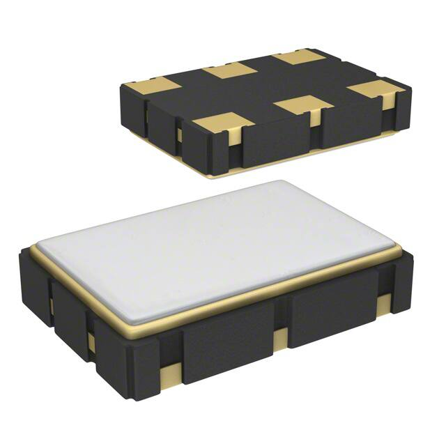
Ultra Series™ Crystal Oscillator (VCXO)
Si565 Data Sheet
Ultra Low Jitter Any-Frequency VCXO (100 fs), 0.2 to 3000
MHz
KEY FEATURES
• Available with any frequency from 200 kHz to
3000 MHz
The Si565 Ultra Series™ voltage-controlled crystal oscillator utilizes Skyworks
Solutions’ advanced 4th generation DSPLL® technology to provide an ultra-low
jitter, low phase noise clock at any output frequency. The device is factory-programmed to any frequency from 0.2 to 3000 MHz with 6 digits
Notes:
1. Contact Skyworks for non-standard configurations.
2. Create custom part numbers at https://www.skyworksinc.com/en/Products/Timing-Oscillators.
3. Min Absolute Pull Range (APR) includes temp stability, initial accuracy, load pulling, VDD variation, and 20 year aging at 70 °C.
a. For best jitter and phase noise performance, always choose the smallest Kv that meets the application’s minimum APR requirements. Unlike SAW-based solutions which require higher Kv values to account for their higher temperature dependence,
the Si56x series provides lower Kv options to minimize noise coupling and jitter in real-world PLL designs.
b. APR is the ability of a VCXO to track a signal over the product lifetime. A VCXO with an APR of ±20 ppm is able to lock to a
clock with a ±20 ppm stability over 20 years over all operating conditions.
c. APR (±) = (0.5 x VDD x tuning slope) - (initial accuracy + temp stability + load pulling + VDD variation + aging).
d. Minimum APR values noted above include absolute worst case values for all parameters.
e. See application note, "AN266: VCXO Tuning Slope (Kv), Stability, and Absolute Pull Range (APR)" for more information.
1.1 Technical Support
Oscillator Phase Noise Lookup Utility
https://www.skyworksinc.com/tools/oscillator-phase-noise
Quality and Reliability
https://www.skyworksinc.com/quality
Development Kits
https://www.skyworksinc.com/en/Products/Timing
2
Skyworks Solutions, Inc. • Phone [781] 376-3000 • Fax [781] 376-3100 • sales@skyworksinc.com • www.skyworksinc.com
Rev. 1.3 • Skyworks Proprietary Information • Products and Product Information are Subject to Change Without Notice • December 3, 2021
2
�Si565 Data Sheet • Electrical Specifications
2. Electrical Specifications
Table 2.1. Electrical Specifications
VDD = 1.8 V, 2.5 or 3.3 V ± 5%, TA = –40 to 85 ºC
Parameter
Temperature Range
Frequency Range
Supply Voltage
Supply Current
Symbol
Min
Typ
Max
Unit
–40
—
85
ºC
LVPECL, LVDS, CML
0.2
—
3000
MHz
HCSL
0.2
—
400
MHz
CMOS, Dual CMOS
0.2
—
250
MHz
3.3 V
3.135
3.3
3.465
V
2.5 V
2.375
2.5
2.625
V
1.8 V
1.71
1.8
1.89
V
LVPECL (output enabled)
—
120
170
mA
LVDS/CML (output enabled)
—
100
140
mA
HCSL (output enabled)
—
95
140
mA
HCSL-Fast (output enabled)
—
103
152
mA
CMOS (output enabled)
—
95
145
mA
Dual CMOS (output enabled)
—
105
155
mA
Tristate Hi-Z (output disabled)
—
83
—
mA
-40 to 85 °C
–20
—
20
ppm
LVPECL/LVDS/CML
—
—
350
ps
CMOS / Dual CMOS
(CL = 5 pF)
—
0.5
1.5
ns
HCSL, FCLK > 50 MHz
—
—
550
ps
HCSL-Fast, FCLK > 50 MHz
—
—
275
ps
All formats
45
—
55
%
TA
FCLK
VDD
IDD
Temperature Stability1
Rise/Fall Time
(20% to 80% VPP)
Test Condition/Comment
TR/TF
Duty Cycle
DC
Output Enable (OE)2
VIH
0.7 × VDD
—
—
V
VIL
—
—
0.3 × VDD
V
Powerup Time
Powerup VDD Ramp Rate
LVPECL Output Option3
3
TD
Output Disable Time, FCLK > 10 MHz
—
—
3
µs
TE
Output Enable Time, FCLK > 10 MHz
—
—
20
µs
tOSC
Time from 0.9 × VDD until output frequency (FCLK) within spec
—
—
10
ms
VRAMP
Fastest VDD ramp rate allowed on
startup
—
—
100
V/ms
VOC
Mid-level
VDD – 1.42
—
VDD – 1.25
V
VO
Swing (diff, FCLK ≤ 1.5 GHz)
1.1
—
1.9
VPP
Swing (diff, FCLK > 1.5 GHz)6
0.55
—
1.7
VPP
Skyworks Solutions, Inc. • Phone [781] 376-3000 • Fax [781] 376-3100 • sales@skyworksinc.com • www.skyworksinc.com
Rev. 1.3 • Skyworks Proprietary Information • Products and Product Information are Subject to Change Without Notice • December 3, 2021
3
�Si565 Data Sheet • Electrical Specifications
Parameter
LVDS Output Option4
Symbol
Test Condition/Comment
Min
Typ
Max
Unit
VOC
Mid-level (2.5 V, 3.3 V VDD)
1.125
1.20
1.275
V
Mid-level (1.8 V VDD)
0.8
0.9
1.0
V
Swing (diff, FCLK ≤ 1.4 GHz)
0.6
0.7
0.9
VPP
Swing (diff, FCLK > 1.4 GHz)6
0.25
0.5
0.8
VPP
VOH
Output voltage high
660
800
850
mV
VOL
Output voltage low
–150
0
150
mV
VC
Crossing voltage
250
410
550
mV
VO
Swing (diff, FCLK ≤ 1.5 GHz)
0.6
0.8
1.0
VPP
Swing (diff, FCLK > 1.5 GHz)6
0.3
0.55
0.9
VPP
VOH
IOH = 8/6/4 mA for 3.3/2.5/1.8 V VDD
0.85 × VDD
—
—
V
VOL
IOL = 8/6/4 mA for 3.3/2.5/1.8 V VDD
—
—
0.15 × VDD
V
VO
HCSL Output Option5
HCSL-Fast Output Option5
CML Output Option (AC-Coupled)
CMOS Output Option
Notes:
1. Min APR includes temperature stability, initial accuracy, load pulling, VDD variation, and aging for 20 yrs at 70 ºC.
2. OE includes a 50 kΩ pull-up to VDD for OE active high, or includes a 50 kΩ pull-down to GND for OE active low.
3. Rterm = 50 Ω to VDD – 2.0 V (see Figure 4.1). Additional DC current from the output driver will flow through the 50 Ω resistors,
resulting in a shift in common mode voltage. The measurements in this table have accounted for this.
4. Rterm = 100 Ω (differential) (see Figure 4.2).
5. Rterm = 50 Ω to GND (see Figure 4.2).
6. Refer to the figure below for Typical Clock Output Swing Amplitudes vs Frequency.
Figure 2.1. Typical Clock Output Swing Amplitudes vs. Frequency
4
Skyworks Solutions, Inc. • Phone [781] 376-3000 • Fax [781] 376-3100 • sales@skyworksinc.com • www.skyworksinc.com
Rev. 1.3 • Skyworks Proprietary Information • Products and Product Information are Subject to Change Without Notice • December 3, 2021
4
�Si565 Data Sheet • Electrical Specifications
Table 2.2. VC Control Voltage Input
VDD = 1.8, 2.5 or 3.3 V ± 5%, TA = –40 to 85 ºC
Parameter
Symbol
Control Voltage Range
VC
Control Voltage Tuning Slope
(Vc = 10% VDD to 90% VDD)
Kv
Kv Variation
Test Condition
Positive slope, ordering option
Kv_var
Best Straight Line fit
Min
Typ
Max
Unit
0.1 x
VDD
VDD/2
0.9 x
VDD
V
60, 75, 105, 150, 180, 225
ppm/V
—
—
±10
%
–1.5
±0.5
+1.5
%
Control Voltage Linearity
LVC
Modulation Bandwidth
BW
—
10
—
kHz
Vc Input Impedance
ZVC
500
—
—
kΩ
Table 2.3. Clock Output Phase Jitter and PSNR
VDD = 1.8 V, 2.5 or 3.3 V ± 5%, TA = –40 to 85 ºC
Parameter
Phase Jitter (RMS, 12 kHz - 20 MHz)1
All Differential Formats, FCLK ≥ 200 MHz
Phase Jitter (RMS, 12 kHz - 20 MHz) 1
All Diff Formats, 100 MHz ≤ FCLK < 200 MHz
Phase Jitter (RMS, 12 kHz - 20 MHz)1
LVDS, FCLK = 156.25 MHz
Phase Jitter (RMS, 12 kHz - 20 MHz)1
CMOS / Dual CMOS Formats
5
Symbol
Test Condition/Comment
Min
Typ
Max
Unit
ϕJ
Kv = 60 ppm/V
—
100
150
fs
Kv = 75 ppm/V
—
103
—
fs
Kv = 105 ppm/V
—
110
—
fs
Kv = 150 ppm/V
—
123
—
fs
Kv = 180 ppm/V
—
132
—
fs
Kv = 225 ppm/V
—
150
—
fs
Kv = 60 ppm/V
—
115
180
fs
Kv = 75 ppm/V
—
118
—
fs
Kv = 105 ppm/V
—
125
—
fs
Kv = 150 ppm/V
—
138
—
fs
Kv = 180 ppm/V
—
147
—
fs
Kv = 225 ppm/V
—
165
—
fs
Kv = 60 ppm/V
—
110
130
fs
Kv = 75 ppm/V
—
113
—
fs
Kv = 105 ppm/V
—
120
—
fs
Kv = 150 ppm/V
—
133
—
fs
Kv = 180 ppm/V
—
142
—
fs
Kv = 225 ppm/V
—
160
—
fs
10 MHz ≤ FCLK < 250 MHz
—
200
—
fs
ϕJ
ϕJ
ϕJ
Skyworks Solutions, Inc. • Phone [781] 376-3000 • Fax [781] 376-3100 • sales@skyworksinc.com • www.skyworksinc.com
Rev. 1.3 • Skyworks Proprietary Information • Products and Product Information are Subject to Change Without Notice • December 3, 2021
5
�Si565 Data Sheet • Electrical Specifications
Parameter
Spurs Induced by External Power Supply
Noise, 50 mVpp Ripple. LVDS 156.25 MHz
Output
Symbol
Test Condition/Comment
Min
Typ
PSNR
100 kHz sine wave
-83
200 kHz sine wave
-83
500 kHz sine wave
-82
1 MHz sine wave
-85
Max
Unit
dBc
Note:
1. Guaranteed by characterization. Jitter inclusive of any spurs.
Table 2.4. 3.2 x 5 mm Clock Output Phase Noise (Typical)
6
Offset Frequency (f)
156.25 MHz LVDS
200 MHz LVDS
644.53125 MHz LVDS
100 Hz
–73
–71
–60
1 kHz
–102
–102
–93
10 kHz
–130
–128
–118
100 kHz
–141
–139
–129
1 MHz
–150
–148
–138
10 MHz
–159
–160
–153
20 MHz
–160
–162
–154
Offset Frequency (f)
156.25 MHz
LVPECL
200 MHz
LVPECL
644.53125 MHz
LVPECL
100 Hz
–72
–71
–60
1 kHz
–103
–101
–92
10 kHz
–130
–127
–117
100 kHz
–142
–139
–129
1 MHz
–150
–148
–138
10 MHz
–160
–162
–154
20 MHz
–161
–162
–156
Unit
dBc/Hz
Unit
dBc/Hz
Skyworks Solutions, Inc. • Phone [781] 376-3000 • Fax [781] 376-3100 • sales@skyworksinc.com • www.skyworksinc.com
Rev. 1.3 • Skyworks Proprietary Information • Products and Product Information are Subject to Change Without Notice • December 3, 2021
6
�Si565 Data Sheet • Electrical Specifications
Figure 2.2. Phase Jitter vs. Output Frequency
Phase jitter measured with Agilent E5052 using a differential-to-single ended converter (balun or buffer). Measurements collected for
>700 commonly used frequencies. Phase noise plots for specific frequencies are available using our free, online Oscillator Phase Noise
Lookup Tool at https://www.skyworksinc.com/en/Products/Timing-Oscillators.
7
Skyworks Solutions, Inc. • Phone [781] 376-3000 • Fax [781] 376-3100 • sales@skyworksinc.com • www.skyworksinc.com
Rev. 1.3 • Skyworks Proprietary Information • Products and Product Information are Subject to Change Without Notice • December 3, 2021
7
�Si565 Data Sheet • Electrical Specifications
Table 2.5. Environmental Compliance and Package Information
Parameter
Test Condition
Mechanical Shock
MIL-STD-883, Method 2002
Mechanical Vibration
MIL-STD-883, Method 2007
Solderability
MIL-STD-883, Method 2003
Gross and Fine Leak
MIL-STD-883, Method 1014
Resistance to Solder Heat
MIL-STD-883, Method 2036
Moisture Sensitivity Level (MSL): 3.2 x 5, 5 x 7 packages
1
Moisture Sensitivity Level (MSL): 2.5 x 3.2 package
2
Contact Pads: 3.2x5, 5x7 packages
Au/Ni (0.3 - 1.0 µm / 1.27 - 8.89 µm)
Contact Pads: 2.5x3.2 packages
Au/Pd/Ni (0.03 - 0.12 µm / 0.1 - 0.2 µm / 3.0 - 8.0 µm)
Note:
1. For additional product information not listed in the data sheet (e.g. RoHS Certifications, MDDS data, qualification data, REACH
Declarations, ECCN codes, etc.), refer to our "Corporate Request For Information" portal found here: www.skyworksinc.com/quality.
Table 2.6. Thermal Conditions1
Max Junction Temperature = 125° C
Package
2.5 x 3.2 mm
6-pin DFN2
3.2 × 5 mm
6-pin CLCC
5 × 7 mm
6-pin CLCC
Parameter
Symbol
Test Condition
Value
Unit
Thermal Resistance Junction to Ambient
ΘJA
Still Air, 85 °C
72
ºC/W
Thermal Parameter Junction to Board
ΨJB
Still Air, 85 °C
38
ºC/W
Thermal Parameter Junction to Top Center
ΨJT
Still Air, 85 °C
15
ºC/W
Thermal Resistance Junction to Ambient
ΘJA
Still Air, 85 °C
55
ºC/W
Thermal Parameter Junction to Board
ΨJB
Still Air, 85 °C
20
ºC/W
Thermal Parameter Junction to Top Center
ΨJT
Still Air, 85 °C
20
ºC/W
Thermal Resistance Junction to Ambient
ΘJA
Still Air, 85 °C
53
ºC/W
Thermal Parameter Junction to Board
ΨJB
Still Air, 85 °C
26
ºC/W
Thermal Parameter Junction to Top Center
ΨJT
Still Air, 85 °C
26
ºC/W
Note:
1. Based on PCB Dimensions: 4.5" x 7", PCB Thickness: 1.6 mm, Number of Cu Layers: 4.
2. For best 2.5x3.2mm thermal performance, use 2 GND vias as shown in the Si5xxUC-EVB eval board layout
8
Skyworks Solutions, Inc. • Phone [781] 376-3000 • Fax [781] 376-3100 • sales@skyworksinc.com • www.skyworksinc.com
Rev. 1.3 • Skyworks Proprietary Information • Products and Product Information are Subject to Change Without Notice • December 3, 2021
8
�Si565 Data Sheet • Electrical Specifications
Table 2.7. Absolute Maximum Ratings1
Parameter
Symbol
Rating
Unit
TAMAX
95
ºC
TS
–55 to 125
ºC
Supply Voltage
VDD
–0.5 to 3.8
ºC
Input Voltage
VIN
–0.5 to VDD + 0.3
V
ESD HBM (JESD22-A114)
HBM
2.0
kV
Solder Temperature2
TPEAK
260
ºC
TP
20–40
sec
Maximum Operating Temp.
Storage Temperature
Solder Time at TPEAK2
Notes:
1. Stresses beyond those listed in this table may cause permanent damage to the device. Functional operation specification
compliance is not implied at these conditions. Exposure to maximum rating conditions for extended periods may affect device
reliability.
2. The device is compliant with JEDEC J-STD-020.
9
Skyworks Solutions, Inc. • Phone [781] 376-3000 • Fax [781] 376-3100 • sales@skyworksinc.com • www.skyworksinc.com
Rev. 1.3 • Skyworks Proprietary Information • Products and Product Information are Subject to Change Without Notice • December 3, 2021
9
�Si565 Data Sheet • Dual CMOS Buffer
3. Dual CMOS Buffer
Dual CMOS output format ordering options support either complementary or in-phase signals for two identical frequency outputs. This
feature enables replacement of multiple VCXOs with a single Si565 device.
~
~
Complementary
Outputs
In-Phase
Outputs
Figure 3.1. Integrated 1:2 CMOS Buffer Supports Complementary or In-Phase Outputs
10
Skyworks Solutions, Inc. • Phone [781] 376-3000 • Fax [781] 376-3100 • sales@skyworksinc.com • www.skyworksinc.com
Rev. 1.3 • Skyworks Proprietary Information • Products and Product Information are Subject to Change Without Notice • December 3, 2021
10
�Si565 Data Sheet • Recommended Output Terminations
4. Recommended Output Terminations
The output drivers support both AC-coupled and DC-coupled terminations as shown in figures below.
VDD
VDD (3.3V, 2.5V)
CLK+
Rp
R1
R1
CLK+
50 Ω
CLK-
Si56x
VDD
VDD (3.3V, 2.5V)
Rp
R2
R2
LVPECL
Receiver
VDD (3.3V, 2.5V)
CLK+
CLK-
Si56x
Rp
50 Ω
Rp
R2
VDD (3.3V, 2.5V)
R1
CLK+
50 Ω
VTT
LVPECL
Receiver
LVPECL
Receiver
AC-Coupled LVPECL - 50 Ω w/VTT Bias
50 Ω
VDD – 2.0V
CLK-
50 Ω
R2
R2
DC-Coupled LVPECL – Thevenin Termination
50 Ω
VDD
50 Ω
Si56x
AC-Coupled LVPECL – Thevenin Termination
R1
50 Ω
CLK-
50 Ω
R1
50 Ω
50 Ω
50 Ω
Si56x
LVPECL
Receiver
DC-Coupled LVPECL - 50 Ω w/VTT Bias
Figure 4.1. LVPECL Output Terminations
AC-Coupled LVPECL
Termination Resistor Values
11
DC-Coupled LVPECL
Termination Resistor Values
VDD
R1
R2
Rp
VDD
R1
R2
3.3 V
82.5 Ω
127 Ω
130 Ω
3.3 V
127 Ω
82.5 Ω
2.5 V
62.5 Ω
250 Ω
90 Ω
2.5 V
250 Ω
62.5 Ω
Skyworks Solutions, Inc. • Phone [781] 376-3000 • Fax [781] 376-3100 • sales@skyworksinc.com • www.skyworksinc.com
Rev. 1.3 • Skyworks Proprietary Information • Products and Product Information are Subject to Change Without Notice • December 3, 2021
11
�Si565 Data Sheet • Recommended Output Terminations
(3.3V, 2.5V, 1.8V)
VDD
CLK+
(3.3V, 2.5V, 1.8V)
VDD
50 Ω
CLK+ 33 Ω
100 Ω
CLK50 Ω
Si56x
LVDS
Receiver
CLK+
50 Ω
HCSL
Receiver
Source Terminated HCSL
(3.3V, 2.5V, 1.8V)
VDD
50 Ω
CLK+
100 Ω
CLK50 Ω
Si56x
50 Ω
50 Ω
Si56x
DC-Coupled LVDS
(3.3V, 2.5V, 1.8V)
VDD
50 Ω
CLK- 33 Ω
50 Ω
CLK-
LVDS
Receiver
50 Ω
50 Ω
Si56x
AC-Coupled LVDS
50 Ω
HCSL
Receiver
Destination Terminated HCSL
Figure 4.2. LVDS and HCSL Output Terminations
(3.3V, 2.5V, 1.8V)
VDD
CLK+
VDD (3.3V, 2.5V, 1.8V)
50 Ω
CLK
10 Ω
100 Ω
CLK-
NC
50 Ω
Si56x
CML
Receiver
CLK+
Si56x
Single CMOS Termination
VDD (3.3V, 2.5V, 1.8V)
50 Ω
50 Ω
CLK+
50 Ω
CLK-
VCM
CLK-
CMOS
Receiver
Si56x
CML Termination without VCM
(3.3V, 2.5V, 1.8V)
VDD
50 Ω
50 Ω
CML
Receiver
CML Termination with VCM
10 Ω
10 Ω
50 Ω
50 Ω
Si56x
CMOS
Receivers
Dual CMOS Termination
Figure 4.3. CML and CMOS Output Terminations
12
Skyworks Solutions, Inc. • Phone [781] 376-3000 • Fax [781] 376-3100 • sales@skyworksinc.com • www.skyworksinc.com
Rev. 1.3 • Skyworks Proprietary Information • Products and Product Information are Subject to Change Without Notice • December 3, 2021
12
�Si565 Data Sheet • Package Outline
5. Package Outline
5.1 Package Outline (5×7 mm)
The figure below illustrates the package details for the 5×7 mm Si565. The table below lists the values for the dimensions shown in the
illustration.
Figure 5.1. Si565 (5×7 mm) Outline Diagram
Table 5.1. Package Diagram Dimensions (mm)
Dimension
Min
Nom
Max
Dimension
Min
Nom
Max
A
1.13
1.28
1.43
L
1.17
1.27
1.37
A2
0.50
0.55
0.60
L1
0.05
0.10
0.15
A3
0.50
0.55
0.60
p
1.70
—
1.90
b
1.30
1.40
1.50
R
0.70 REF
c
0.50
0.60
0.70
aaa
0.15
bbb
0.15
ccc
0.08
D
D1
5.00 BSC
4.30
4.40
4.50
e
2.54 BSC
ddd
0.10
E
7.00 BSC
eee
0.05
E1
6.10
6.20
6.30
Notes:
1. All dimensions shown are in millimeters (mm) unless otherwise noted.
2. Dimensioning and Tolerancing per ANSI Y14.5M-1994.
13
Skyworks Solutions, Inc. • Phone [781] 376-3000 • Fax [781] 376-3100 • sales@skyworksinc.com • www.skyworksinc.com
Rev. 1.3 • Skyworks Proprietary Information • Products and Product Information are Subject to Change Without Notice • December 3, 2021
13
�Si565 Data Sheet • Package Outline
5.2 Package Outline (3.2×5 mm)
The figure below illustrates the package details for the 3.2×5 mm Si565. The table below lists the values for the dimensions shown in
the illustration.
Figure 5.2. Si565 (3.2×5 mm) Outline Diagram
Table 5.2. Package Diagram Dimensions (mm)
Dimension
Min
Nom
Max
A
1.06
1.17
1.33
b
0.54
0.64
0.74
c
0.35
0.45
0.55
D
D1
3.20 BSC
2.55
2.60
e
1.27 BSC
E
5.00 BSC
2.65
E1
4.35
4.40
4.45
H
0.45
0.55
0.65
L
0.80
0.90
1.00
L1
0.05
0.10
0.15
p
1.36
1.46
1.56
R
0.32 REF
aaa
0.15
bbb
0.15
ccc
0.08
ddd
0.10
eee
0.05
Notes:
1. All dimensions shown are in millimeters (mm) unless otherwise noted.
2. Dimensioning and Tolerancing per ANSI Y14.5M-1994.
14
Skyworks Solutions, Inc. • Phone [781] 376-3000 • Fax [781] 376-3100 • sales@skyworksinc.com • www.skyworksinc.com
Rev. 1.3 • Skyworks Proprietary Information • Products and Product Information are Subject to Change Without Notice • December 3, 2021
14
�Si565 Data Sheet • Package Outline
5.3 Package Outline (2.5x3.2 mm)
The figure below illustrates the package details for the 2.5x3.2 mm Si565. The table below lists the values for the dimensions shown in
the illustration.
Figure 5.3. Si565 (2.5×3.2 mm) Outline Diagram
Table 5.3. Package Diagram Dimensions (mm)
Dimension
Min
Nom
Max
A
0.90
0.95
1.00
A1
0.36 REF
A2
0.53 REF
W
0.55
0.60
D
3.2 BSC
E
2.5 BSC
e
1.10 BSC
L
0.65
0.70
n
5
D1
2.2 BSC
E1
1.589 BSC
aaa
0.10
bbb
0.10
ddd
0.08
0.65
0.75
Notes:
1. The dimensions in parentheses are reference.
2. All dimensions in millimeters (mm).
3. Dimensioning and Tolerancing per ANSI Y14.5M-1994.
15
Skyworks Solutions, Inc. • Phone [781] 376-3000 • Fax [781] 376-3100 • sales@skyworksinc.com • www.skyworksinc.com
Rev. 1.3 • Skyworks Proprietary Information • Products and Product Information are Subject to Change Without Notice • December 3, 2021
15
�Si565 Data Sheet • PCB Land Pattern
6. PCB Land Pattern
6.1 PCB Land Pattern (5×7 mm)
The figure below illustrates the 5×7 mm PCB land pattern for the Si565. The table below lists the values for the dimensions shown in
the illustration.
Figure 6.1. Si565 (5×7 mm) PCB Land Pattern
Table 6.1. PCB Land Pattern Dimensions (mm)
Dimension
(mm)
C1
4.20
E
2.54
X1
1.55
Y1
1.95
Notes:
General
1. All dimensions shown are in millimeters (mm) unless otherwise noted.
2. Dimensioning and Tolerancing is per the ANSI Y14.5M-1994 specification.
3. This Land Pattern Design is based on the IPC-7351 guidelines.
4. All dimensions shown are at Maximum Material Condition (MMC). Least Material Condition (LMC) is calculated based on a
Fabrication Allowance of 0.05 mm.
Solder Mask Design
1. All metal pads are to be non-solder mask defined (NSMD). Clearance between the solder mask and the metal pad is to be 60 µm
minimum, all the way around the pad.
Stencil Design
1. A stainless steel, laser-cut and electro-polished stencil with trapezoidal walls should be used to assure good solder paste release.
2. The stencil thickness should be 0.125 mm (5 mils).
3. The ratio of stencil aperture to land pad size should be 1:1.
Card Assembly
1. A No-Clean, Type-3 solder paste is recommended.
2. The recommended card reflow profile is per the JEDEC/IPC J-STD-020 specification for Small Body Components.
16
Skyworks Solutions, Inc. • Phone [781] 376-3000 • Fax [781] 376-3100 • sales@skyworksinc.com • www.skyworksinc.com
Rev. 1.3 • Skyworks Proprietary Information • Products and Product Information are Subject to Change Without Notice • December 3, 2021
16
�Si565 Data Sheet • PCB Land Pattern
6.2 PCB Land Pattern (3.2×5 mm)
The figure below illustrates the 3.2×5.0 mm PCB land pattern for the Si565. The table below lists the values for the dimensions shown
in the illustration.
Figure 6.2. Si565 (3.2×5 mm) PCB Land Pattern
Table 6.2. PCB Land Pattern Dimensions (mm)
Dimension
(mm)
C1
2.60
E
1.27
X1
0.80
Y1
1.70
Notes:
General
1. All dimensions shown are in millimeters (mm) unless otherwise noted.
2. Dimensioning and Tolerancing is per the ANSI Y14.5M-1994 specification.
3. This Land Pattern Design is based on the IPC-7351 guidelines.
4. All dimensions shown are at Maximum Material Condition (MMC). Least Material Condition (LMC) is calculated based on a
Fabrication Allowance of 0.05 mm.
Solder Mask Design
1. All metal pads are to be non-solder mask defined (NSMD). Clearance between the solder mask and the metal pad is to be 60 µm
minimum, all the way around the pad.
Stencil Design
1. A stainless steel, laser-cut and electro-polished stencil with trapezoidal walls should be used to assure good solder paste release.
2. The stencil thickness should be 0.125 mm (5 mils).
3. The ratio of stencil aperture to land pad size should be 1:1.
Card Assembly
1. A No-Clean, Type-3 solder paste is recommended.
2. The recommended card reflow profile is per the JEDEC/IPC J-STD-020 specification for Small Body Components.
17
Skyworks Solutions, Inc. • Phone [781] 376-3000 • Fax [781] 376-3100 • sales@skyworksinc.com • www.skyworksinc.com
Rev. 1.3 • Skyworks Proprietary Information • Products and Product Information are Subject to Change Without Notice • December 3, 2021
17
�Si565 Data Sheet • PCB Land Pattern
6.3 PCB Land Pattern (2.5×3.2 mm)
The figure below illustrates the 2.5×3.2 mm PCB land pattern for the Si565. The table below lists the values for the dimensions shown
in the illustration.
Figure 6.3. Si565 (2.5×3.2 mm) PCB Land Pattern
Table 6.3. PCB Land Pattern Dimensions (mm)
Dimension
Description
Value (mm)
X1
Width - leads on long sides
0.85
Y1
Height - leads on long sides
0.7
D1
Pitch in X directions of XLY1 leads
1.639
E1
Lead pitch XLY1 leads
1.10
Notes: The following notes and stencil design are shared as recommendations only. A customer or user may find it necessary to use
different parameters and fine-tune their SMT process as required for their application and tooling.
General
1. All dimensions shown are in millimeters (mm) unless otherwise noted.
2. Dimensioning and Tolerancing is per the ANSI Y14.5M-1994 specification.
3. This Land Pattern Design is based on the IPC-7351 guidelines.
4. All dimensions shown are at Maximum Material Condition (MMC). Least Material Condition (LMC) is calculated based on a
Fabrication Allowance of 0.05 mm.
Solder Mask Design
1. All metal pads are to be non-solder mask defined (NSMD). Clearance between the solder mask and the metal pad is to be 60 µm
minimum, all the way around the pad.
Stencil Design
1. A stainless steel, laser-cut and electro-polished stencil with trapezoidal walls should be used to assure good solder paste release.
2. The stencil thickness should be 0.125 mm (5 mils).
3. The ratio of stencil aperture to land pad size should be 0.8:1 for the pads.
Card Assembly
1. A No-Clean, Type-3 solder paste is recommended.
2. The recommended card reflow profile is per the JEDEC/IPC J-STD-020 specification for Small Body Components.
18
Skyworks Solutions, Inc. • Phone [781] 376-3000 • Fax [781] 376-3100 • sales@skyworksinc.com • www.skyworksinc.com
Rev. 1.3 • Skyworks Proprietary Information • Products and Product Information are Subject to Change Without Notice • December 3, 2021
18
�Si565 Data Sheet • Top Markings
7. Top Markings
7.1 Top Marking (5x7 and 3.2x5 Packages)
The figure below illustrates the mark specification for the Si565 5x7 and 3.2x5 package sizes. The table below lists the line information.
Figure 7.1. Mark Specification
Table 7.1. Si565 Top Mark Description
Line
Position
Description
1
1–8
"Si565", xxx = Ordering Option 1, Option 2, Option 3 (e.g. Si565AAA)
2
1–7
Frequency Code
(e.g. 100M000 or 6-digit custom code as described in the Ordering Guide)
3
19
Trace Code
Position 1
Pin 1 orientation mark (dot)
Position 2
Product Revision (C)
Position 3–5
Tiny Trace Code (3 alphanumeric characters per assembly release instructions)
Position 6–7
Year (last two digits of the year), to be assigned by assembly site (ex: 2017 = 17)
Position 8–9
Calendar Work Week number (1–53), to be assigned by assembly site
Skyworks Solutions, Inc. • Phone [781] 376-3000 • Fax [781] 376-3100 • sales@skyworksinc.com • www.skyworksinc.com
Rev. 1.3 • Skyworks Proprietary Information • Products and Product Information are Subject to Change Without Notice • December 3, 2021
19
�Si565 Data Sheet • Top Markings
7.2 Top Marking (2.5x3.2 Package)
The figure below illustrates the mark specification for the Si565 2.5x3.2 package sizes. The table below lists the line information.
NC CC CC
T TTT TT
Y Y WW
Figure 7.2. Mark Specification
Table 7.2. Si565 Top Mark Description
Line
Position
1
1–6
2
20
N = Si565, CCCCC = Custom Mark Code
Trace Code
1–6
3
Description
Position 1
Six-digit trace code per assembly release instructions
Pin 1 orientation mark (dot)
Position 2–3
Year (last two digits of the year), to be assigned by assembly site (exp: 2017 = 17)
Position 4–5
Calendar Work Week number (1–53), to be assigned by assembly site
Skyworks Solutions, Inc. • Phone [781] 376-3000 • Fax [781] 376-3100 • sales@skyworksinc.com • www.skyworksinc.com
Rev. 1.3 • Skyworks Proprietary Information • Products and Product Information are Subject to Change Without Notice • December 3, 2021
20
�Si565 Data Sheet • Revision History
8. Revision History
Revision 1.3
June, 2021
• Updated Ordering Guide and Top Mark for Rev C silicon.
• Added HCSL-Fast (faster tR/tF) ordering option.
• Updated Table 2.1, Powerup VDD Ramp Rate.
Revision 1.2
September, 2020
• Added 2.5 x 3.2 mm package option.
• Updated Table 2.1, Powerup VDD Ramp Rate and LVDS Swing.
Revision 1.0
June, 2018
• Initial draft
21
Skyworks Solutions, Inc. • Phone [781] 376-3000 • Fax [781] 376-3100 • sales@skyworksinc.com • www.skyworksinc.com
Rev. 1.3 • Skyworks Proprietary Information • Products and Product Information are Subject to Change Without Notice • December 3, 2021
21
�ClockBuilder Pro
Customize Skyworks clock generators,
jitter attenuators and network
synchronizers with a single tool. With
CBPro you can control evaluation
boards, access documentation, request
a custom part number, export for
in-system programming and more!
www.skyworksinc.com/CBPro
Portfolio
SW/HW
Quality
Support & Resources
www.skyworksinc.com/ia/timing
www.skyworksinc.com/CBPro
www.skyworksinc.com/quality
www.skyworksinc.com/support
Copyright © 2021 Skyworks Solutions, Inc. All Rights Reserved.
Information in this document is provided in connection with Skyworks Solutions, Inc. (“Skyworks”) products or services. These materials, including the
information contained herein, are provided by Skyworks as a service to its customers and may be used for informational purposes only by the customer.
Skyworks assumes no responsibility for errors or omissions in these materials or the information contained herein. Skyworks may change its documentation,
products, services, specifications or product descriptions at any time, without notice. Skyworks makes no commitment to update the materials or
information and shall have no responsibility whatsoever for conflicts, incompatibilities, or other difficulties arising from any future changes.
No license, whether express, implied, by estoppel or otherwise, is granted to any intellectual property rights by this document. Skyworks assumes no liability
for any materials, products or information provided hereunder, including the sale, distribution, reproduction or use of Skyworks products, information or
materials, except as may be provided in Skyworks’ Terms and Conditions of Sale.
THE MATERIALS, PRODUCTS AND INFORMATION ARE PROVIDED “AS IS” WITHOUT WARRANTY OF ANY KIND, WHETHER EXPRESS, IMPLIED, STATUTORY, OR
OTHERWISE, INCLUDING FITNESS FOR A PARTICULAR PURPOSE OR USE, MERCHANTABILITY, PERFORMANCE, QUALITY OR NON-INFRINGEMENT OF ANY
INTELLECTUAL PROPERTY RIGHT; ALL SUCH WARRANTIES ARE HEREBY EXPRESSLY DISCLAIMED. SKYWORKS DOES NOT WARRANT THE ACCURACY OR
COMPLETENESS OF THE INFORMATION, TEXT, GRAPHICS OR OTHER ITEMS CONTAINED WITHIN THESE MATERIALS. SKYWORKS SHALL NOT BE LIABLE FOR
ANY DAMAGES, INCLUDING BUT NOT LIMITED TO ANY SPECIAL, INDIRECT, INCIDENTAL, STATUTORY, OR CONSEQUENTIAL DAMAGES, INCLUDING WITHOUT
LIMITATION, LOST REVENUES OR LOST PROFITS THAT MAY RESULT FROM THE USE OF THE MATERIALS OR INFORMATION, WHETHER OR NOT THE RECIPIENT
OF MATERIALS HAS BEEN ADVISED OF THE POSSIBILITY OF SUCH DAMAGE.
Skyworks products are not intended for use in medical, lifesaving or life-sustaining applications, or other equipment in which the failure of the Skyworks
products could lead to personal injury, death, physical or environmental damage. Skyworks customers using or selling Skyworks products for use in such
applications do so at their own risk and agree to fully indemnify Skyworks for any damages resulting from such improper use or sale.
Customers are responsible for their products and applications using Skyworks products, which may deviate from published specifications as a result of
design defects, errors, or operation of products outside of published parameters or design specifications. Customers should include design and operating
safeguards to minimize these and other risks. Skyworks assumes no liability for applications assistance, customer product design, or damage to any
equipment resulting from the use of Skyworks products outside of Skyworks’ published specifications or parameters.
Skyworks, the Skyworks symbol, Sky5®, SkyOne®, SkyBlue™, Skyworks Green™, Clockbuilder®, DSPLL®, ISOmodem®, ProSLIC®, and SiPHY® are trademarks or
registered trademarks of Skyworks Solutions, Inc. or its subsidiaries in the United States and other countries. Third-party brands and names are for
identification purposes only and are the property of their respective owners. Additional information, including relevant terms and conditions, posted at
www.skyworksinc.com, are incorporated by reference.
Skyworks Solutions, Inc. | Nasdaq: SWKS | sales@skyworksinc.com | www.skyworksinc.com
USA: 781-376-3000 | Asia: 886-2-2735 0399 | Europe: 33 (0)1 43548540 |
�


 工商网监
湘ICP备2023018690号
工商网监
湘ICP备2023018690号

