Si 514
A NY -F REQ U E N C Y I 2 C P R O GRAMMABLE X O (100 kH Z
TO
250 MH Z )
Features
Programmable to any frequency
from 100 kHz to 250 MHz
0.026 ppb frequency tuning
resolution
Glitch suppression on OE, power
on and frequency transitions
Low jitter operation
2- to 4-week lead times
Total stability includes 10-year
aging
Comprehensive production test
coverage includes crystal ESR and
DLD
On-chip LDO for power supply
noise filtering
3.3, 2.5, or 1.8 V operation
Differential (LVPECL, LVDS,
HCSL) or CMOS output options
Optional integrated 1:2 CMOS
fanout buffer
Industry standard 5x7, 3.2x5, and
2.5x3.2 mm packages
–40 to 85 oC operation
Applications
All-digital PLLs
DAC+ VCXO replacement
SONET/SDH/OTN
3G-SDI/HD-SDI/SDI
Datacom
Industrial automation
FPGA/ASIC clock generation
FPGA synchronization
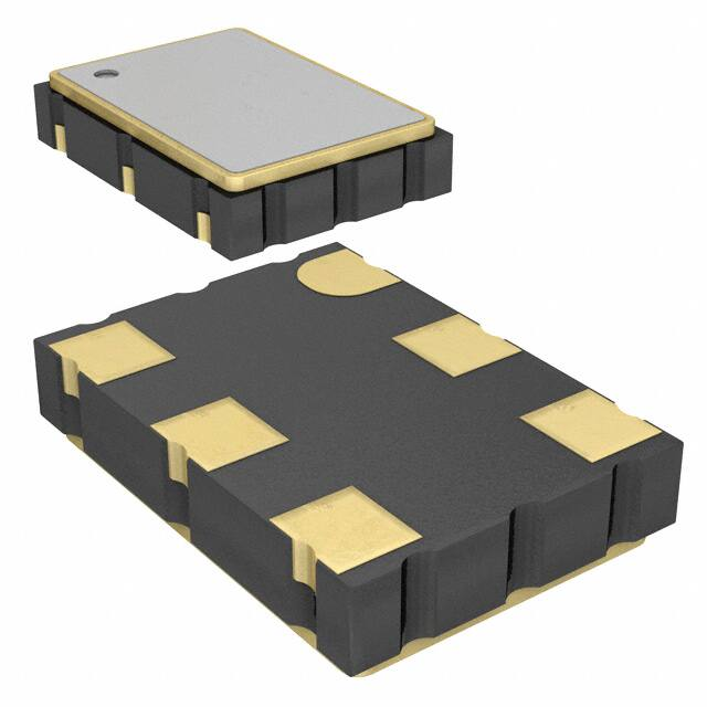
Si5602
5x7mm, 3.2x5mm
2.5x3.2mm
Ordering Information:
See page 28.
Pin Assignments:
See page 27.
SDA
1
6
VDD
Description
SCL
2
5
CLK–
The Si514 user-programmable I2C XO utilizes Skyworks Solutions' advanced PLL
technology to provide any frequency from 100 kHz to 250 MHz with programming
resolution of 0.026 parts per billion. The Si514 uses a single integrated crystal and
Skyworks Solutions’ proprietary DSPLL synthesizer to generate any frequency
across this range using simple I2C commands. Ultra-fine tuning resolution replaces
DACs and VCXOs with an all-digital PLL solution that improves performance where
synchronization is necessary or in free-running reference clock applications. This
solution provides superior supply noise rejection, simplifying low jitter clock
generation in noisy environments. Crystal ESR and DLD are individually
production-tested to guarantee performance and enhance reliability.
The Si514 is factory-configurable for a wide variety of user specifications, including
startup frequency, I2C address, supply voltage, output format, and stability. Specific
configurations are factory-programmed at time of shipment, eliminating long lead
times and non-recurring engineering charges associated with custom frequency
oscillators.
GND
3
4
CLK+
Functional Block Diagram
Skyworks Solutions, Inc. • Phone [781] 376-3000 • Fax [781] 376-3100 • sales@skyworksinc.com • www.skyworksinc.com
Rev. 1.2 • Skyworks Proprietary Information • Products and Product Information are Subject to Change Without Notice • August 12, 2021
�Si 514
TA B L E
Section
OF
C ONTENTS
Page
1. Electrical Specifications . . . . . . . . . . . . . . . . . . . . . . . . . . . . . . . . . . . . . . . . . . . . . . . . . . . 3
2. Solder Reflow and Rework Requirements for 2.5x3.2 mm Packages . . . . . . . . . . . . . . 11
3. Functional Description . . . . . . . . . . . . . . . . . . . . . . . . . . . . . . . . . . . . . . . . . . . . . . . . . . . 12
3.1. Programming a New Output Frequency . . . . . . . . . . . . . . . . . . . . . . . . . . . . . . . . . . 12
3.2. Programming a Small Frequency Change (sub ±1000 ppm) . . . . . . . . . . . . . . . . . . 13
3.3. Programming a Large Frequency Change (> ±1000 ppm) . . . . . . . . . . . . . . . . . . . .14
4. All-Digital PLL Applications . . . . . . . . . . . . . . . . . . . . . . . . . . . . . . . . . . . . . . . . . . . . . . .18
5. User Interface . . . . . . . . . . . . . . . . . . . . . . . . . . . . . . . . . . . . . . . . . . . . . . . . . . . . . . . . . . . 19
5.1. Register Map . . . . . . . . . . . . . . . . . . . . . . . . . . . . . . . . . . . . . . . . . . . . . . . . . . . . . . . 19
5.2. Register Detailed Description . . . . . . . . . . . . . . . . . . . . . . . . . . . . . . . . . . . . . . . . . . 20
5.3. I2C Interface . . . . . . . . . . . . . . . . . . . . . . . . . . . . . . . . . . . . . . . . . . . . . . . . . . . . . . . 25
6. Pin Descriptions . . . . . . . . . . . . . . . . . . . . . . . . . . . . . . . . . . . . . . . . . . . . . . . . . . . . . . . . .27
6.1. Dual CMOS (1:2 Fanout Buffer) . . . . . . . . . . . . . . . . . . . . . . . . . . . . . . . . . . . . . . . . 27
7. Ordering Information . . . . . . . . . . . . . . . . . . . . . . . . . . . . . . . . . . . . . . . . . . . . . . . . . . . . . 28
8. Package Outline Diagram: 5 x 7 mm, 6-pin . . . . . . . . . . . . . . . . . . . . . . . . . . . . . . . . . . . 29
9. PCB Land Pattern: 5 x 7 mm, 6-pin . . . . . . . . . . . . . . . . . . . . . . . . . . . . . . . . . . . . . . . . . . 30
10. Package Outline Diagram: 3.2 x 5.0 mm, 6-pin . . . . . . . . . . . . . . . . . . . . . . . . . . . . . . . 31
11. PCB Land Pattern: 3.2 x 5.0 mm, 6-pin . . . . . . . . . . . . . . . . . . . . . . . . . . . . . . . . . . . . . . 32
12. Package Outline Diagram: 2.5 x 3.2 mm, 6-pin . . . . . . . . . . . . . . . . . . . . . . . . . . . . . . . 33
13. PCB Land Pattern: 2.5 x 3.2 mm, 6-pin . . . . . . . . . . . . . . . . . . . . . . . . . . . . . . . . . . . . . . 35
14. Top Marking . . . . . . . . . . . . . . . . . . . . . . . . . . . . . . . . . . . . . . . . . . . . . . . . . . . . . . . . . . . 36
14.1. Si514 Top Marking . . . . . . . . . . . . . . . . . . . . . . . . . . . . . . . . . . . . . . . . . . . . . . . . . 36
14.2. Top Marking Explanation . . . . . . . . . . . . . . . . . . . . . . . . . . . . . . . . . . . . . . . . . . . . 36
Document Change List . . . . . . . . . . . . . . . . . . . . . . . . . . . . . . . . . . . . . . . . . . . . . . . . . . . . . 37
2
Skyworks Solutions, Inc. • Phone [781] 376-3000 • Fax [781] 376-3100 • sales@skyworksinc.com • www.skyworksinc.com
Rev. 1.2 • Skyworks Proprietary Information • Products and Product Information are Subject to Change Without Notice • August 12, 2021
�Si514
1. Electrical Specifications
Table 1. Operating Specifications
VDD = 1.8 V ±5%, 2.5 or 3.3 V ±10%, TA = –40 to +85 oC
Parameter
Supply Voltage
Supply Current
Symbol
Test Condition
Min
Typ
Max
Units
VDD
3.3 V option
2.97
3.3
3.63
V
2.5 V option
2.25
2.5
2.75
V
1.8 V option
1.71
1.8
1.89
V
CMOS, 100 MHz,
single-ended
—
21
26
mA
LVDS
(output enabled)
—
19
23
mA
LVPECL
(output enabled)
—
39
43
mA
HCSL
(output enabled)
—
41
44
mA
Tristate
(output disabled)
—
—
18
mA
–40
—
85
o
IDD
Operating Temperature
TA
C
Table 2. Input Characteristics
VDD = 1.8 V ±5%, 2.5 or 3.3 V ±10%, TA = –40 to +85 oC
Parameter
Symbol
Test Condition
Min
Typ
Max
Units
SDA, SCL Input Voltage High
VIH
0.80 x VDD
—
—
V
SDA, SCL Input Voltage Low
VIL
—
—
0.20 x VDD
V
Skyworks Solutions, Inc. • Phone [781] 376-3000 • Fax [781] 376-3100 • sales@skyworksinc.com • www.skyworksinc.com
3
Rev. 1.2 • Skyworks Proprietary Information • Products and Product Information are Subject to Change Without Notice • August 12, 2021
�Si 514
Table 3. Output Clock Frequency Characteristics
VDD = 1.8 V ±5%, 2.5 or 3.3 V ±10%, TA = –40 to +85 oC
Parameter
Programmable
Frequency Range
Frequency
Reprogramming
Resolution
Symbol
Test Condition
Min
Typ
Max
Units
FO
CMOS, Dual CMOS
0.1
—
212.5
MHz
FO
LVDS/LVPECL/HCSL
0.1
—
250
MHz
—
0.026
—
ppb
MRES
Frequency Range for
Small Frequency Change
(Continuous Glitchless
Output)
Settling time for Small
Frequency Change
From center frequency
–1000
—
+1000
ppm
±1000 ppm from
center frequency
—
—
10
ms
Frequency Stability Grade C
–30
—
+30
ppm
Frequency Stability Grade B
–50
—
+50
ppm
Frequency Stability Grade A
–100
—
+100
ppm
Frequency Stability Grade C
–20
—
+20
ppm
Frequency Stability Grade B
–25
—
+25
ppm
Frequency Stability Grade A
–50
—
+50
ppm
Temperature Stability
Startup Time
TSU
Minimum VDD until output
frequency (FO) within specification
—
—
10
ms
Disable Time
TD
FO < 10 MHz
—
—
40
µs
FO 10 MHz
—
—
5
µs
FO < 10 MHz
—
—
60
µs
FO 10 MHz
—
—
20
µs
Enable Time
TE
*Note: Total stability includes initial accuracy, operating temperature, supply voltage change, load change, shock and
vibration (not under operation), and 10 years aging at 40 oC.
4
Skyworks Solutions, Inc. • Phone [781] 376-3000 • Fax [781] 376-3100 • sales@skyworksinc.com • www.skyworksinc.com
Rev. 1.2 • Skyworks Proprietary Information • Products and Product Information are Subject to Change Without Notice • August 12, 2021
�Si514
Table 4. Output Clock Levels and Symmetry
VDD = 1.8 V ±5%, 2.5 or 3.3 V ±10%, TA = –40 to +85 oC
Parameter
Symbol
Test Condition
Min
Typ
Max
Units
CMOS Output Logic
High
VOH
0.85 x VDD
—
—
V
CMOS Output Logic
Low
VOL
—
—
0.15 x VDD
V
CMOS Output Logic
High Drive
IOH
3.3 V
–8
—
—
mA
2.5 V
–6
—
—
mA
1.8 V
–4
—
—
mA
3.3 V
8
—
—
mA
2.5 V
6
—
—
mA
1.8 V
4
—
—
mA
0.1 to 125 MHz,
CL = 15 pF
—
0.8
1.2
ns
0.1 to 212.5 MHz,
CL = no load
—
0.6
0.9
ns
CMOS Output Logic
Low Drive
IOL
CMOS Output
Rise/Fall Time
(20 to 80% VDD)
TR/TF
LVPECL/HCSL Output Rise/Fall Time
(20 to 80% VDD)
LVDS Output Rise/Fall
Time (20 to 80% VDD)
LVPECL Output Common Mode
TR/TF
—
—
565
ps
TR/TF
—
—
800
ps
VOC
50 to VDD – 2 V, single-ended
—
VDD –
1.4 V
—
V
LVPECL Output Swing
VO
50 to VDD – 2 V, single-ended
0.55
0.8
0.90
VPPSE
LVDS Output Common
Mode
VOC
100 line-line, 3.3/2.5 V
1.13
1.23
1.33
V
100 line-line, 1.8 V
0.83
0.92
1.00
V
LVDS Output Swing
VO
Single-ended 100 differential
termination
0.25
0.35
0.45
VPPSE
HCSL Output
Common Mode
HCSL Output Swing
VOC
50 to ground
0.35
0.38
0.42
V
VO
Single-ended
0.58
0.73
0.85
VPPSE
Duty Cycle
DC
48
50
52
%
Skyworks Solutions, Inc. • Phone [781] 376-3000 • Fax [781] 376-3100 • sales@skyworksinc.com • www.skyworksinc.com
5
Rev. 1.2 • Skyworks Proprietary Information • Products and Product Information are Subject to Change Without Notice • August 12, 2021
�Si 514
Table 5. Output Clock Jitter and Phase Noise (LVPECL)
VDD = 2.5 or 3.3 V ±10%, TA = –40 to +85 oC; Output Format = LVPECL
Parameter
Symbol
Test Condition
Min
Typ
Max
Units
Period Jitter (RMS)
JPRMS
10 k samples1
—
—
1.3
ps
Period Jitter (Pk-Pk) JPPKPK
10 k samples1
—
—
11
ps
1.875 MHz to 20 MHz integration
bandwidth2 (brickwall)
—
0.31
0.5
ps
12 kHz to 20 MHz integration bandwidth2
—
0.8
1.0
ps
100 Hz
—
–86
—
dBc/Hz
1 kHz
—
–109
—
dBc/Hz
10 kHz
—
–116
—
dBc/Hz
100 kHz
—
–123
—
dBc/Hz
1 MHz
—
–136
—
dBc/Hz
10 kHz sinusoidal noise
—
3.0
—
ps
100 kHz sinusoidal noise
—
3.5
—
ps
500 kHz sinusoidal noise
—
3.5
—
ps
1 MHz sinusoidal noise
—
3.5
—
ps
LVPECL output, 156.25 MHz,
offset > 10 kHz
—
–75
—
dBc
Phase Jitter (RMS)
Phase Noise,
156.25 MHz
Additive RMS
Jitter Due to Power
Supply Noise3
Spurious
φJ
φN
JPSR
SPR
Notes:
1. Applies to output frequencies: 74.17582, 74.25, 75, 77.76, 100, 106.25, 125, 148.35165, 148.5, 150, 155.52, 156.25,
212.5, 250 MHz.
2. Applies to output frequencies: 100, 106.25, 125, 148.35165, 148.5, 150, 155.52, 156.25, 212.5 and 250 MHz.
3. 156.25 MHz. Increase in jitter on output clock due to sinewave noise added to VDD (2.5/3.3 V = 100 mVPP).
6
Skyworks Solutions, Inc. • Phone [781] 376-3000 • Fax [781] 376-3100 • sales@skyworksinc.com • www.skyworksinc.com
Rev. 1.2 • Skyworks Proprietary Information • Products and Product Information are Subject to Change Without Notice • August 12, 2021
�Si514
Table 6. Output Clock Jitter and Phase Noise (LVDS)
VDD = 1.8 V ±5%, 2.5 or 3.3 V ±10%, TA = –40 to +85 oC; Output Format = LVDS
Symbol
Test Condition
Min
Typ
Max
Unit
Period Jitter
(RMS)
JPRMS
10k samples1
—
—
2.1
ps
Period Jitter
(Pk-Pk)
JPPKPK
10k samples1
—
—
18
ps
Phase Jitter
(RMS)
φJ
1.875 MHz to 20 MHz integration
bandwidth2 (brickwall)
—
0.25
0.55
ps
12 kHz to 20 MHz integration bandwidth2 (brickwall)
—
0.8
1.0
ps
100 Hz
—
–86
—
dBc/Hz
1 kHz
—
–109
—
dBc/Hz
10 kHz
—
–116
—
dBc/Hz
100 kHz
—
–123
—
dBc/Hz
1 MHz
—
–136
—
dBc/Hz
LVPECL output, 156.25 MHz,
offset>10 kHz
—
–75
—
dBc
Parameter
Phase Noise,
156.25 MHz
Spurious
φN
SPR
Notes:
1. Applies to output frequencies: 74.17582, 74.25, 75, 77.76, 100, 106.25, 125, 148.35165, 148.5, 150, 155.52, 156.25,
212.5, 250 MHz.
2. Applies to output frequencies: 100, 106.25, 125, 148.35165, 148.5, 150, 155.52, 156.25, 212.5 and 250 MHz.
Skyworks Solutions, Inc. • Phone [781] 376-3000 • Fax [781] 376-3100 • sales@skyworksinc.com • www.skyworksinc.com
7
Rev. 1.2 • Skyworks Proprietary Information • Products and Product Information are Subject to Change Without Notice • August 12, 2021
�Si 514
Table 7. Output Clock Jitter and Phase Noise (HCSL)
VDD = 1.8 V ±5%, 2.5 or 3.3 V ±10%, TA = –40 to +85 oC; Output Format = HCSL
Symbol
Test Condition
Min
Typ
Max
Unit
Period Jitter
(RMS)
JPRMS
10k samples*
—
—
1.2
ps
Period Jitter
(Pk-Pk)
JPPKPK
10k samples*
—
—
11
ps
Phase Jitter
(RMS)
φJ
1.875 MHz to 20 MHz integration
bandwidth*(brickwall)
—
0.25
0.30
ps
12 kHz to 20 MHz integration bandwidth* (brickwall)
—
0.8
1.0
ps
100 Hz
—
–90
—
dBc/Hz
1 kHz
—
–112
—
dBc/Hz
10 kHz
—
–120
—
dBc/Hz
100 kHz
—
–127
—
dBc/Hz
1 MHz
—
–140
—
dBc/Hz
LVPECL output, 156.25 MHz,
offset>10 kHz
—
–75
—
dBc
Parameter
Phase Noise,
156.25 MHz
Spurious
φN
SPR
*Note: Applies to an output frequency of 100 MHz.
8
Skyworks Solutions, Inc. • Phone [781] 376-3000 • Fax [781] 376-3100 • sales@skyworksinc.com • www.skyworksinc.com
Rev. 1.2 • Skyworks Proprietary Information • Products and Product Information are Subject to Change Without Notice • August 12, 2021
�Si514
Table 8. Output Clock Jitter and Phase Noise (CMOS, Dual CMOS)
VDD = 1.8 V ±5%, 2.5 or 3.3 V ±10%, TA = –40 to +85 oC; Output Format = CMOS, Dual CMOS
Parameter
Symbol
Test Condition
Min
Typ
Max
Unit
φJ
1.875 MHz to 20 MHz integration
bandwidth2 (brickwall)
—
0.25
0.35
ps
12 kHz to 20 MHz integration bandwidth2 (brickwall)
—
0.8
1.0
ps
100 Hz
—
–86
—
dBc/Hz
1 kHz
—
–108
—
dBc/Hz
10 kHz
—
–115
—
dBc/Hz
100 kHz
—
–123
—
dBc/Hz
1 MHz
—
–136
—
dBc/Hz
LVPECL output, 156.25 MHz,
offset>10 kHz
—
–75
—
dBc
Phase Jitter
(RMS)
Phase Noise,
156.25 MHz
Spurious
φN
SPR
Notes:
1. Applies to output frequencies: 74.17582, 74.25, 75, 77.76, 100, 106.25, 125, 148.35165, 148.5, 150, 155.52, 156.25,
212.5 MHz.
2. Applies to output frequencies: 100, 106.25, 125, 148.35165, 148.5, 150, 155.52, 156.25, 212.5 MHz.
Table 9. Environmental Compliance and Package Information
Parameter
Conditions/Test Method
Mechanical Shock
MIL-STD-883, Method 2002
Mechanical Vibration
MIL-STD-883, Method 2007
Solderability
MIL-STD-883, Method 2003
Gross and Fine Leak
MIL-STD-883, Method 1014
Resistance to Solder Heat
MIL-STD-883, Method 2036
Contact Pads
Gold over Nickel
Skyworks Solutions, Inc. • Phone [781] 376-3000 • Fax [781] 376-3100 • sales@skyworksinc.com • www.skyworksinc.com
9
Rev. 1.2 • Skyworks Proprietary Information • Products and Product Information are Subject to Change Without Notice • August 12, 2021
�Si 514
Table 10. Thermal Characteristics
Parameter
Symbol
Test Condition
Value
Units
CLCC, Thermal Resistance Junction to Ambient*
JA
Still air
110
°C/W
2x5 x 3.2 mm, Thermal Resistance Junction to Ambient*
JA
Still air
164
°C/W
*Note: Applies to 5 x 7 and 3.2 x 5 mm packages.
Table 11. Absolute Maximum Ratings1
Parameter
Symbol
Rating
TAMAX
85
TS
–55 to +125
oC
VDD
–0.5 to +3.8
V
VI
–0.5 to VDD + 0.3
V
ESD Sensitivity (HBM, per JESD22-A114)
HBM
2
kV
Soldering Temperature (Pb-free profile)2
TPEAK
260
TP
20–40
Maximum Operating Temperature
Storage Temperature
Supply Voltage
Input Voltage (any input pin)
Soldering Temperature Time at TPEAK (Pb-free profile)2
Units
o
C
o
C
sec
Notes:
1. Stresses beyond those listed in this table may cause permanent damage to the device. Functional operation or
specification compliance is not implied at these conditions. Exposure to maximum rating conditions for extended
periods may affect device reliability.
2. The device is compliant with JEDEC J-STD-020E.
10
Skyworks Solutions, Inc. • Phone [781] 376-3000 • Fax [781] 376-3100 • sales@skyworksinc.com • www.skyworksinc.com
Rev. 1.2 • Skyworks Proprietary Information • Products and Product Information are Subject to Change Without Notice • August 12, 2021
�Si514
2. Solder Reflow and Rework Requirements for 2.5x3.2 mm Packages
Reflow of Skyworks Solutions' components should be done in a manner consistent with the IPC/JEDEC J-STD-20E
standard. The temperature of the package is not to exceed the classification Temperature provided in the standard.
The part should not be within -5°C of the classification or peak reflow temperature (TPEAK) for longer than 30
seconds. Key to maintaining the integrity of the component is providing uniform heating and cooling of the part
during reflow and rework. Uniform heating is achieved through having a preheat soak and controlling the
temperature ramps in the process. J-STD-20E provides minimum and maximum temperatures and times for the
preheat/Soak step that need to be followed, even for rework. The entire assembly area should be heated during
rework. Hot air should be flowed from both the bottom of the board and the top of the component. Heating from the
top only will cause un-even heating of component and can lead to part integrity issues. Temperature Ramp-up rate
are not to exceed 3°C/second. Temperature ramp-down rates from peak to final temperature are not to exceed
6°C/second. Time from 25°C to peak temperature is not to exceed 8 min for Pb-free solders.
Skyworks Solutions, Inc. • Phone [781] 376-3000 • Fax [781] 376-3100 • sales@skyworksinc.com • www.skyworksinc.com
11
Rev. 1.2 • Skyworks Proprietary Information • Products and Product Information are Subject to Change Without Notice • August 12, 2021
�Si 514
3. Functional Description
The Si514 offers system designers a programmable, low jitter XO solution with exceptionally fine frequency tuning
resolution. To enable designers to take full advantage of this flexibility and performance, Skyworks Solutions
provides an easy-to-use evaluation kit and intuitive suite of Windows-based software utilities to simplify the Si514
programming process.
The Si5xx-PROG-EVB kit contains the Programmable Oscillator Software suite and an EVB Driver (USBXpress®)
for use with USB-equipped PCs. Go to
www.skyworksinc.com/en/application-pages/Developers for more information.
Alternatively, “3.1. Programming a New Output Frequency” provides designers a detailed description, along with
examples, of the frequency programming requirements and process for designers who are interested in learning
more about the programming algorithms implemented within the Programmable Oscillator Software suite.
3.1. Programming a New Output Frequency
The output frequency (Fout) is determined by programming the feedback multiplier (M=M_Int.M_Frac), HighSpeed Divider (HS_DIV), and Low-Speed Divider (LS_DIV) according to the following formula:
F XO M
F out = -------------------------------------------------HS_DIV LS_DIV
where F XO = 31.98MHz
Figure 1. Block Diagram of Si514
The value of the feedback multiplier M is adjustable in the following range:
65.04065041 M 78.17385866.
This keeps the VCO frequency within the range of 2080 MHz FVCO 2500 MHz, since the VCO frequency is the
product of the internal fixed-frequency crystal (FXO) and the high-resolution 29-bit fractional multiplier (M). This 29bit resolution of M allows the VCO frequency to have a frequency tuning resolution of 0.026 ppb.
The device comes from the factory with a pre-programmed center frequency within the range of
100 kHz FOUT 250 MHz, as specified by the 6-digit code in the part number. (See section “7. Ordering
Information” for more information.) To change from the factory-programmed frequency to a different value, the user
must follow one of two algorithms based on the magnitude of the frequency change.
12
“Small Frequency Change.” To change the frequency by < ±1000 ppm, the user must keep the same center
frequency and only update the value of M. Refer to section "3.2. Programming a Small Frequency Change (sub
±1000 ppm)" on page 13.
“Large Frequency Change.” To change the frequency by ±1000 ppm, the user must change the center
frequency. This may require updates to the output dividers (HS_DIV and/or LS_DIV) and possibly the LP1 and
Skyworks Solutions, Inc. • Phone [781] 376-3000 • Fax [781] 376-3100 • sales@skyworksinc.com • www.skyworksinc.com
Rev. 1.2 • Skyworks Proprietary Information • Products and Product Information are Subject to Change Without Notice • August 12, 2021
�Si514
LP2 values, in addition to updating the value of M, which requires the VCO to be recalibrated. Refer to section
"3.3. Programming a Large Frequency Change (> ±1000 ppm)" on page 14. Figure 2 provides a graphic
depiction of the difference between small and large frequency changes.
Range of small
frequency change
FCENTER
-1000 ppm
FVCO_MIN
(2080 MHz)
Small Frequency Change
Large Frequency Change
FCENTER
+1000 ppm
FCENTER
F'CENTER
FVCO_MAX
(2500 MHz)
Programming a new center frequency requires a VCO
calibration and the output should be squelched
Figure 2. Small vs. Large Frequency Change Illustration
3.2. Programming a Small Frequency Change (sub ±1000 ppm)
The value of the feedback multiplier, M is the only parameter that needs to be updated for output frequency
changes less than ±1000 ppm from the center frequency (recalibrating the VCO is NOT required). This enables
the output to remain continuous during the change. For example, the output frequency can be swept continuously
between 148.5 MHz and 148.352 MHz (i.e., –0.997 ppm) with no output discontinuities or glitches by changing M
in either multiple steps or in a single step. For small frequency changes, each update of M requires 100 µs to
settle.
Note: It is not possible to implement a frequency change ≥ ±1000 ppm using multiple small frequency changes
without changing the center frequency and recalibrating the VCO.
Use the following procedure to make small frequency changes:
1. If the current value of M is already known, then skip to step 2; else, using the serial port, read the current M
value (Registers 5-9).
2. Calculate the new value of M as follows (all values are in decimal format):
a. Mcurrent = M_Int + M_Frac/229 (Eq 2.2)
b. Mnew = Mcurrent x Fout_new / Fout_current (Eq 2.3)
c. M_Intnew = INT[Mnew]*
(Eq 2.4)
d. M_Fracnew = (Mnew – INT[Mnew]) x 229 (Eq 2.5)
*Where INT[n] rounds n down to the nearest integer (e.g., INT[3.9] = 3)
3. Using the I2C port, write the new value of M_Frac[23:0] (Not all registers need to be updated.)
(Registers: 5, 6, 7)
4. If necessary, write new value of M_Int[2:0] and M_Frac[28:24] register. (Register 8)
5. Write M_Int[8:3]. (Register 9) Frequency changes take effect when M_Int[8:3] is written.
Example 2.1:
An Si514 generating a 148.5 MHz clock must be reconfigured “on-the-fly” to generate a 148.352 MHz clock. This
represents a change of –0.996.633 ppm which is within the ±1000 ppm window.
1. Read the current value of M:
a. Register 5 = 0xD3 (M_Frac[7:0])
b. Register 6 = 0x65 (M_Frac[15:8])
c. Register 7 = 0x7C (M_Frac[23:16])
Skyworks Solutions, Inc. • Phone [781] 376-3000 • Fax [781] 376-3100 • sales@skyworksinc.com • www.skyworksinc.com
13
Rev. 1.2 • Skyworks Proprietary Information • Products and Product Information are Subject to Change Without Notice • August 12, 2021
�Si 514
d.
e.
f.
g.
h.
Register 8 = 0x49 (M_Int[2:0],M_Frac[28:24])
Register 9 = 0x09 (M_Int[8:3])
M_Int = 0b001001010 = 0x4A = 0d74
M_Frac = 0x097C65D3 = 159,147,475
M= M_Int + M_Frac/229 = 74 + 159,147,475/229 = 74.296435272321105
2. Calculate Mnew:
a. Mnew = 74.296435272321105 x 148.352/148.5 = 74.2223889933965
b. M_Intnew = 74 = 0x4A
c. M_Fracnew = 0.2223889933965 x 229 = 119,394,181 = 0x071DCF85
3. Write Mnew to Registers 5-7:
a. Register 5 = 0x85
b. Register 6 = 0xCF
c. Register 7 = 0x1D
4. Write Mnew to Register 8:
a. Register 8 = 0x47
5. Write Mnew to Register 9:
a. Register 9 = 0x09
3.3. Programming a Large Frequency Change (> ±1000 ppm)
Large frequency changes are those that vary the FVCO frequency by an amount greater than ±1000 ppm from an
operating FCENTER. Figure 2 illustrates the difference between large and small frequency changes. Changing from
FCENTER to F'CENTER requires a calibration cycle that resets internal circuitry to establish F'CENTER as the new
operating center frequency. The below steps are recommended when performing large frequency changes:
1. Disable the output: Write OE register bit to a 0 (Register 132, bit2)
2. If using one of the standard frequencies listed in Table 12, then write the new LP1, LP2, M_Frac, M_Int,
HS_DIV and LS_DIV register values according to the table (be sure to write M_Int[8:3] (Register 9) after writing
to the M_Frac registers (Registers 5-8)). Skip to Step 9. If the desired frequency is not in the table, then follow
steps 4-8 below.
3. Determine the minimum value of LS_DIV (minimizing LS_DIV minimizes the number of dividers on the output
stage, thus minimizing jitter) according to the following formula:
a. LS_DIV = FVCO(MIN)/(FOUT x HS_DIV(MAX)) (Eq 2.6)
b. LS_DIV = 2080/(FOUT(MHz) x 1022) (Eq 2.7)
i. Since LS_DIV is restricted to: dividing by 1,2,4,8,16,32, choose the next largest value over the
result derived in Eq 2.7 (e.g., if result is 4.135, choose LS_DIV = 8)
4. Determine the minimum value for HS_DIV (this optimizes timing margins)
a. HS_DIV(MIN) = FVCO(MIN)/(FOUT x LS_DIV) (Eq 2.8)
b. HS_DIV(MIN) = 2080/(FOUT(MHz) x LS_DIV) (Eq 2.9)
i.HS_DIV(MIN) will be the next even number greater than or equal to the result derived in Eq 2.9
(keeping in the range of 10-1022)
Note: SPEED_GRADE_MIN (Reg 48) ≤ LS_DIV x HS_DIV ≤ SPEED_GRADE_MAX (Reg 49); If outside this range, the output
will be forced to the disabled state.
5. Determine a value for M according to the following formula (all values are in decimal format):
a. M = LS_DIV x HS_DIV x FOUT/FXO (Eq 2.10)
b. M = LS_DIV x HS_DIV x FOUT(MHz)/31.98 (Eq 2.11)
c. M_Int = INT[M] (Eq 2.12)
d. M_Frac = (M – INT[M]) x 229 (Eq 2.13)
14
Skyworks Solutions, Inc. • Phone [781] 376-3000 • Fax [781] 376-3100 • sales@skyworksinc.com • www.skyworksinc.com
Rev. 1.2 • Skyworks Proprietary Information • Products and Product Information are Subject to Change Without Notice • August 12, 2021
�Si514
Table 12. Standard Frequency Table
DEC
HEX
Fout
(MHz)
M
M_INT
M_FRAC
HSDIV LSDIV LP1 LP2 M_INTX M_FRACX HSDIVX LSDIVX
LP1_X LP2_X
0.100000
65.04065041
65
21824021
650
5
2
2
41
14D0215
28A
5
2
2
1.544000
65.08167605
65
43849494
674
1
2
2
41
29D1716
2A2
1
2
2
2.048000
65.06466542
65
34716981
1016
0
2
2
41
211BD35
3F8
0
2
2
4.096000
65.06466542
65
34716981
508
0
2
2
41
211BD35
1FC
0
2
2
4.915200
65.16712946
65
89726943
424
0
2
2
41
5591FDF
1A8
0
2
2
19.440000 65.65103189
65
349520087
108
0
2
3
41
14D540D7
6C
0
2
3
24.576000 66.08930582
66
47945695
86
0
2
3
42
2DB97DF
56
0
2
3
25.000000 65.66604128
65
357578187
84
0
2
3
41
155035CB
54
0
2
3
27.000000 65.85365854
65
458304437
78
0
2
3
41
1B512BB5
4E
0
2
3
38.880000 65.65103189
65
349520087
54
0
2
3
41
14D540D7
36
0
2
3
44.736000 67.14596623
67
78365022
48
0
2
3
43
4ABC15E
30
0
2
3
54.000000 67.54221388
67
291098862
40
0
2
3
43
1159D0EE
28
0
2
3
62.500000 66.44777986
66
240399983
34
0
2
3
42
E54366F
22
0
2
3
65.536000 65.57698562
65
309766794
32
0
2
3
41
1276AA8A
20
0
2
3
74.175824 69.58332458
69
313169998
30
0
3
3
45
12AA984E
1E
0
3
3
74.250000 69.65290807
69
350527350
30
0
3
3
45
14E49F76
1E
0
3
3
77.760000 68.08255159
68
44319550
28
0
3
3
44
2A4433E
1C
0
3
3
106.250000 66.44777986
66
240399983
20
0
2
3
42
E54366F
14
0
2
3
125.000000 70.3564728
70
191379875
18
0
3
3
46
B6839A3
12
0
3
3
148.351648 74.22221288
74
119299633
16
0
3
4
4A
71C5E31
10
0
3
4
148.500000 74.29643527
74
159147475
16
0
3
4
4A
97C65D3
10
0
3
4
150.000000 65.66604128
65
357578187
14
0
2
3
41
155035CB
E
0
2
3
155.520000 68.08255159
68
44319550
14
0
3
3
44
2A4433E
E
0
3
3
156.250000 68.40212633
68
215889929
14
0
3
3
44
CDE3809
E
0
3
3
212.500000 66.44777986
66
240399983
10
0
2
3
42
E54366F
A
0
2
3
250.000000 78.17385866
78
93339658
10
0
4
4
4E
590400A
A
0
4
4
Skyworks Solutions, Inc. • Phone [781] 376-3000 • Fax [781] 376-3100 • sales@skyworksinc.com • www.skyworksinc.com
15
Rev. 1.2 • Skyworks Proprietary Information • Products and Product Information are Subject to Change Without Notice • August 12, 2021
�Si 514
6. Determine values for LP1 and LP2 according to Table 13:
Table 13. LP1, LP2 Values
Fvco_max
Fvco_min
M_max
M_min
LP1
LP2
2500000000.00000
2425467616.18572
78.173858662
75.843265046
4
4
2425467616.18572
2332545246.89005
75.843265046
72.937624981
3
4
2332545246.89005
2170155235.53450
72.937624981
67.859763463
3
3
2170155235.53450
2087014168.27005
67.859763463
65.259980246
2
3
2087014168.27005
2080000000.00000
65.259980246
65.040650407
2
2
7. Write new LP1, LP2, M_Frac, M_Int, HS_DIV and LS_DIV register values (be sure to write M_Int[8:3] (Register
9) after writing to the M_Frac registers (Registers 5-8)
8. Write FCAL (Register 132, bit 0) to a 1 (this bit auto-resets, so it will always read as 0).
9. Enable the output: Write OE register bit to a 1.
The Si514 does not automatically detect large frequency changes. The user needs to assert the FCAL register bit
to initiate the calibration cycle required to re-center the VCO around the new frequency. Large frequency changes
are discontinuous and output may skip to intermediate frequencies or generate glitches. Resetting the OE bit
before FCAL will prevent intermediate frequencies from appearing on the output while Si514 completes a
calibration cycle and settles to F'CENTER. Settling time for large frequency changes is 10 msec maximum.
Example 2.2:
The user has a part that is programmed with SPEED_GRADE_MIN = 20 and SPEED_GRADE_MAX = 250 that is
programmed from the factory for FOUT = 50 MHz and wants to change to an STS-1 rate of 51.84 MHz. This
represents a change of +36,800 ppm which exceeds ±1000 ppm and therefore requires a large frequency change
process.
1. Write Reg 132, bit 2 to a 0 to disable the output.
2. Since 51.84 MHz is not in Table 2.1, the divider parameters must be calculated.
3. Calculate LS_DIV by using Eq 2.7:
a. LS_DIV = 2080/(51.84 x 1022) = 0.039
b. Since 0.039 < 1, use a divide-by-one (bypass), therefore LS_DIV = 0
4. Calculate HS_DIV(MIN) by using Eq 2.9:
a. HS_DIV(MIN) = 2080/(51.84 x 1) = 40.123
b. Since 40.123 > 40, use HS_DIV(MIN) = 42 = 0x2A
5. From Eq 2.11:
a. M = 1 x 42 x 51.84/31.98 = 68.08255159474
b. M_Int = 68 = 0x44
c. M_Frac = 0.08255259474 x 229 = 44,320,087 = 0x2A44557
6. From Table 2.2:
a. LP1 = 3
b. LP2 = 3
16
Skyworks Solutions, Inc. • Phone [781] 376-3000 • Fax [781] 376-3100 • sales@skyworksinc.com • www.skyworksinc.com
Rev. 1.2 • Skyworks Proprietary Information • Products and Product Information are Subject to Change Without Notice • August 12, 2021
�Si514
7. Write Registers 0, 5-11:
a. Register 0 = 0x33
b. Register 5 = 0x57 (M_Frac[7:0])
c. Register 6 = 0x45 (M_Frac[15:8])
d. Register 7 = 0xA4 (M_Frac[23:16])
e. Register 8 = 0x42 (M_Int[2:0],M_Frac[28:24])
f. Register 9 = 0x05 (M_Int[8:3])
g. Register 10 = 0x2A
h. Register 11 = 0x00
8. Calibrate the VCO by writing Register 132, bit 0 to a 1.
9. Enable the output by writing Register 132, bit 2 to a 1.
Skyworks Solutions, Inc. • Phone [781] 376-3000 • Fax [781] 376-3100 • sales@skyworksinc.com • www.skyworksinc.com
17
Rev. 1.2 • Skyworks Proprietary Information • Products and Product Information are Subject to Change Without Notice • August 12, 2021
�Si 514
4. All-Digital PLL Applications
The Si514 uses a high resolution divider M that enables fine frequency adjustments with resolution better than
0.026 parts per billion. Fine frequency adjustments are useful when making frequency corrections that compensate
for changing ambient conditions, long term aging or when locking the Si514 to an input clock reference. Figure 3
shows a typical implementation using a system IC such as an FPGA to control the output of the Si514 in a phaselocked application. Refer to “AN575: An Introduction to FPGA-Based ADPLLs” for more information.
Fin
÷
Si514
SCL
I2C Control
SDA
PD
Loop
Filter
Command
Conversion
I2C
Master
CLK_OUT
Any Frequency
DSPLL
FB
÷
FPGA
Figure 3. All-Digital PLL Application Using Si514 with Dual CMOS Output
Since small frequency changes must be within ±1000 ppm of the center frequency, HS_DIV and LS_DIV remain
constant. The below expression can be used to calculate a new M2 divider value based on a desired output
frequency shift, where ∆FOUT is in ppm.
–6
M 2 = M 1 1 – F OUT 10
Some systems, particularly those that use feedback control, can simplify the computation by implementing an
approximate frequency change based on toggling a bit position or adding/subtracting a bit to the existing M_Frac
value. Since M ranges approximately ±10% between 65.04065041 and 78.17385866, the effect of changing
M_Frac by a single bit depends only slightly on the absolute value of M.
For M=71 near the midpoint of the range, toggling M_Frac[0] changes the output frequency by 0.026 ppb. Each
higher order bit doubles the influence such that toggling M_Frac[1] is 0.052 ppb, M_Frac[2] is 0.1 ppb, etc. Figure 4
shows this trend across multiple registers generalized to M_Frac[N]. Coarse changes greater than ±1.7 ppm are
possible but most applications require finer transitions. Toggling each bit involves incrementing or decrementing
the bit position. Writing M_Int[8:3] in register 9 completes the operation.
1.7ppm
6.7ppb
M = 71.000000000000
M_Int[8:0] = 000100111
0.026ppb
M_Frac[28:0] = 00000000000000000000000000000
M_Frac[23:16] = 00000000
M_Frac[15:8] = 00000000
M_Frac[7:0] = 00000000
Figure 4. Output Frequency Change When Toggling M_Frac[N], M=71
18
Skyworks Solutions, Inc. • Phone [781] 376-3000 • Fax [781] 376-3100 • sales@skyworksinc.com • www.skyworksinc.com
Rev. 1.2 • Skyworks Proprietary Information • Products and Product Information are Subject to Change Without Notice • August 12, 2021
�Si514
5. User Interface
5.1. Register Map
Table 14 displays the Si514 user register map. Registers not shown are reserved. Registers with reserved bits are
read-modify-write.
Table 14. User Register Map
Address
Bit
7
0
6
5
4
3
LP1[3:0]
M_Frac [7:0]
6
M_Frac [15:8]
7
M_Frac [23:16]
8
M_Int [2:0]
0
M_Frac [28:24]
9
M_Int [8:3]
10
HS_DIV [7:0]
11
LS_DIV [ 2:0]
14
132
1
LP2[3:0]
5
128
2
HS_DIV [9:8]
OE_STATE [1:0]
RST
OE
FCAL
Skyworks Solutions, Inc. • Phone [781] 376-3000 • Fax [781] 376-3100 • sales@skyworksinc.com • www.skyworksinc.com
19
Rev. 1.2 • Skyworks Proprietary Information • Products and Product Information are Subject to Change Without Notice • August 12, 2021
�Si 514
5.2. Register Detailed Description
Note: Registers not shown are reserved. Registers with reserved bits are read-modify-write.
Register 0.
Bit
7
6
5
4
3
2
1
Name
LP1[3:0]
LP2[3:0]
Type
R/W
R/W
Default
Varies
Varies
Bit
Name
7:4
LP1[3:0]
Sets loop compensation factor LP1. Value depends on VCO frequency.
3:0
LP2[3:0]
Sets loop compensation factor LP2. Value depends on VCO frequency.
0
Function
Register 5.
Bit
7
6
5
4
3
Name
M_Frac[7:0]
Type
R/W
Default
Varies
Bit
Name
7:0
M_Frac[7:0]
2
1
0
Function
Fractional part of feedback divider M that sets up the output frequency. Frequency
updates take effect when M_Int[8:3] is written.
Register 6.
Bit
6
5
4
3
Name
M_Frac[15:8]
Type
R/W
Default
Varies
Bit
7:0
20
7
Name
2
1
0
Function
M_Frac[15:8] Fractional part of feedback divider M that sets up the output frequency. Frequency
updates take effect when M_Int[8:3] is written.
Skyworks Solutions, Inc. • Phone [781] 376-3000 • Fax [781] 376-3100 • sales@skyworksinc.com • www.skyworksinc.com
Rev. 1.2 • Skyworks Proprietary Information • Products and Product Information are Subject to Change Without Notice • August 12, 2021
�Si514
Register 7.
Bit
7
6
5
4
3
Name
M_Frac[23:16]
Type
R/W
Default
Varies
Bit
Name
7:0
2
1
0
Function
M_Frac[23:16] Fractional part of feedback divider M that sets up the output frequency. Frequency
updates take effect when M_Int[8:3] is written.
Register 8.
Bit
7
6
5
4
3
2
Name
M_Int[2:0]
M_Frac[28:24]
Type
R/W
R/W
Default
Varies
Varies
1
0
Bit
Name
Function
7:5
M_Int[2:0]
Integer part of feedback divider M that sets the output frequency. Frequency updates
take effect when M_Int[8:3] is written.
4:0
M_Frac[28:24] Fractional part of feedback divider M that sets up the output frequency. Frequency
updates take effect when M_Int[8:3] is written.
Skyworks Solutions, Inc. • Phone [781] 376-3000 • Fax [781] 376-3100 • sales@skyworksinc.com • www.skyworksinc.com
21
Rev. 1.2 • Skyworks Proprietary Information • Products and Product Information are Subject to Change Without Notice • August 12, 2021
�Si 514
Register 9.
Bit
7
6
5
4
3
Name
2
1
0
M_Int[8:3]
Type
R/W
R/W
R/W
Default
Varies
Bit
Name
Function
7:6
Reserved
5:0
M_Int[8:3]
Integer part of feedback divider M that sets the output frequency. Frequency updates
take effect when M_Int[8:3] is written.
Register 10.
Bit
22
7
6
5
4
3
Name
HS_DIV[7:0]
Type
R/W
Default
Varies
2
1
0
Bit
Name
Function
7:0
HS_DIV[7:0]
Integer divider that divides VCO frequency and provides output to LS_DIV. Follow the
large frequency change procedure when updating. The allowed values are even numbers in the range from 10 to 1022 (i.e., 10, 12, 14, 16, ...., 1022). The decimal value
represents the actual divide value (i.e. 12 means divide-by-12).
Skyworks Solutions, Inc. • Phone [781] 376-3000 • Fax [781] 376-3100 • sales@skyworksinc.com • www.skyworksinc.com
Rev. 1.2 • Skyworks Proprietary Information • Products and Product Information are Subject to Change Without Notice • August 12, 2021
�Si514
Register 11.
Bit
7
6
Name
5
4
3
2
LS_DIV[2:0]
Type
R/W
R/W
R/W
R/W
Varies
Bit
Name
7
Reserved
6:4
LS_DIV[2:0]
3:2
Reserved
1:0
HS_DIV[9:8]
0
HS_DIV[9:8]
R/W
Default
1
Varies
Function
Last output divider stage. Used during large frequency changes. To update, follow
large frequency change procedure. LS_DIV value updates asynchronously.
000: divide-by-1
001: divide-by-2
010: divide-by-4
011: divide-by-8
100: divide-by-16
101: divide-by-32
All others reserved.
Integer divider that divides VCO frequency and provides output to LS-DIV. Follow the
large frequency change procedure when updating. The allowed values are even numbers in the range from 10 to 1022 (i.e., 10, 12, 14, 16, ..., 1022). The decimal value
represents the actual divide value (i.e., 12 means divide-by-12).
Register 14.
Bit
7
6
Name
Type
5
4
3
2
1
0
R/W
R/W
R/W
R/W
OE_STATE[1:0]
R/W
Default
R/W
R/W
0
Bit
Name
7:6
Reserved
5:4
OE_STATE[1:0]
3:0
Reserved
0
Function
Sets logic state of output when output disabled.
00: high impedance
10: logic low when output disabled
01: logic high when output disabled
11: reserved
Skyworks Solutions, Inc. • Phone [781] 376-3000 • Fax [781] 376-3100 • sales@skyworksinc.com • www.skyworksinc.com
23
Rev. 1.2 • Skyworks Proprietary Information • Products and Product Information are Subject to Change Without Notice • August 12, 2021
�Si 514
Register 128.
Bit
7
Name
RST
Type
R/W
Default
0
Bit
Name
7
RST
6:0
Reserved
6
5
4
3
2
1
0
R/W
R/W
R/W
R/W
R/W
R/W
R/W
1
0
Function
Global Reset.
Resets all register values to default values. Self-clearing.
Register 132.
Bit
7
6
5
4
3
Name
Type
OE
R/W
R/W
R/W
R/W
R/W
Default
24
2
R/W
1
Bit
Name
7:3
Reserved
2
OE
1
Reserved
0
FCAL
FCAL
R/W
R/W
0
Function
Output Enable.
OE can stop in high, low or high impedance state.
1: Output driver enabled.
0: Output driver powered down. OE_STATE register determines output state when
disabled.
Initiates frequency calibration cycle. Necessary when making large frequency
changes. Frequency calibration cycle takes 10 msec maximum. To prevent intermediate frequencies on the output, set disable output using OE register. Self-clearing.
Skyworks Solutions, Inc. • Phone [781] 376-3000 • Fax [781] 376-3100 • sales@skyworksinc.com • www.skyworksinc.com
Rev. 1.2 • Skyworks Proprietary Information • Products and Product Information are Subject to Change Without Notice • August 12, 2021
�Si514
5.3. I2C Interface
Configuration and operation of the Si514 is controlled by reading and writing to the RAM space using the I2C
interface. The device operates in slave mode with 7-bit addressing and can operate in Standard-Mode (100 kbps)
or Fast-Mode (400 kbps). Burst data transfer with auto address increments are also supported.
The I2C bus consists of a bidirectional serial data line (SDA) and a serial clock input (SCL). Both the SDA and SCL
pins must be connected to the VDD supply via an external pull-up as recommended by the I2C specification. The
Si514 7-bit I2C slave address is user-customized during the part number configuration process. See "6. Pin
Descriptions" on page 27 for more details.
Data is transferred MSB first in 8-bit words as specified by the I2C specification. A write command consists of a 7bit device (slave) address + a write bit, an 8-bit register address, and 8 bits of data as shown in Figure 5.
A write burst operation is also shown where every additional data word is written using an auto-incremented
address.
Write Operation – Single Byte
S Slv Addr [6:0]
0
A Reg Addr [7:0] A
Data [7:0]
A
P
A
Data [7:0]
Write Operation - Burst (Auto Address Increment)
S Slv Addr [6:0]
0
A Reg Addr [7:0] A
Data [7:0]
A
P
Reg Addr +1
From slave to master
From master to slave
1 – Read
0 – Write
A – Acknowledge (SDA LOW)
N – Not Acknowledge (SDA HIGH)
S – START condition
P – STOP condition
Figure 5. I2C Write Operation
A read operation is performed in two stages. A data write is used to set the register address, then a data read is
performed to retrieve the data from the set address. A read burst operation is also supported. This is shown in
Figure 6.
Skyworks Solutions, Inc. • Phone [781] 376-3000 • Fax [781] 376-3100 • sales@skyworksinc.com • www.skyworksinc.com
25
Rev. 1.2 • Skyworks Proprietary Information • Products and Product Information are Subject to Change Without Notice • August 12, 2021
�Si 514
Read Operation – Single Byte
S Slv Addr [6:0]
0
A Reg Addr [7:0] A
S Slv Addr [6:0]
1
A
Data [7:0]
P
N P
Read Operation - Burst (Auto Address Increment)
S Slv Addr [6:0]
0
A Reg Addr [7:0] A
S Slv Addr [6:0]
1
A
Data [7:0]
A
P
Data [7:0]
N P
Reg Addr +1
From slave to master
From master to slave
1 – Read
0 – Write
A – Acknowledge (SDA LOW)
N – Not Acknowledge (SDA HIGH)
S – START condition
P – STOP condition
Figure 6. I2C Read Operation
The timing specifications and timing diagram for the I2C bus is compatible with the I2C-Bus standard. SDA timeout
is supported for compatibility with SMBus interfaces.
The I2C bus can be operated at a bus voltage of 1.71 to 3.63 V and is 3.3 V tolerant.
26
Skyworks Solutions, Inc. • Phone [781] 376-3000 • Fax [781] 376-3100 • sales@skyworksinc.com • www.skyworksinc.com
Rev. 1.2 • Skyworks Proprietary Information • Products and Product Information are Subject to Change Without Notice • August 12, 2021
�Si514
6. Pin Descriptions
SDA
1
6
VDD
SCL
2
5
CLK–
GND
3
4
CLK+
Table 15. Si514 Pin Descriptions
Pin
Name
Function
1
SDA
I2C Serial Data.
2
SCL
I2C Serial Clock.
3
GND
Electrical and Case Ground.
4
CLK+
Clock Output.
5
CLK-
Complementary clock output (LVPECL, LVDS, HCSL, and
Complementary dual CMOS formats).
Clock output for in-phase dual CMOS format.
No connect (N/C) for single-ended CMOS format.
6
VDD
Power Supply Voltage.
6.1. Dual CMOS (1:2 Fanout Buffer)
Dual CMOS output format ordering options support either complementary or in-phase output signals. This feature
enables replacement of multiple XOs with a single Si514 device.
~
~
Complementary
Outputs
In-Phase
Outputs
Figure 7. Integrated 1:2 CMOS Buffer Supports Complementary or In-Phase Outputs
Skyworks Solutions, Inc. • Phone [781] 376-3000 • Fax [781] 376-3100 • sales@skyworksinc.com • www.skyworksinc.com
27
Rev. 1.2 • Skyworks Proprietary Information • Products and Product Information are Subject to Change Without Notice • August 12, 2021
�Si 514
7. Ordering Information
The Si514 supports a wide variety of options including startup frequency, stability, output format, and VDD. Specific
device configurations are programmed into the Si514 at time of shipment. Configurations can be specified using
the Part Number Configuration chart below. Skyworks Solutions provides a web browser-based part number
configuration utility to simplify this process. To access this tool refer to www.skyworksinc.com/products/timingoscillators and click “Customize” in the product table. The Si514 XO series is supplied in industry-standard, RoHScompliant, 2.5 x 3.2 mm, 3.2 x 5.0 mm, and 5 x 7 mm packages. Tape and reel packaging is an ordering option.
Series
Output Format
Package
514
LVPECL, LVDS, HCSL,
CMOS, Dual CMOS
6-pin
1st Option Code:
Output Format
A = Revision: A
G = Temp Range: -40°C to 85°C
R = Tape & Reel; Blank = Coil Tape
514 X X X XXXXXX X AGR
VDD
Output Format
LVPECL
A
3.3V
B
3.3V
LVDS
C
3.3V
CMOS
D
3.3V
HCSL
E
2.5V
LVPECL
F
2.5V
LVDS
G
2.5V
CMOS
H
2.5V
HCSL
J
1.8V
LVDS
K
1.8V
CMOS
L
1.8V
HCSL
M
3.3V
Dual CMOS (In-phase)
N
3.3V
Dual CMOS (Complementary)
P
2.5V
Dual CMOS (In-phase)
Q
2.5V
Dual CMOS (Complementary)
R
1.8V
Dual CMOS (In-phase)
S
1.8V
Dual CMOS (Complementary)
3rd Option Code:
Frequency Grade
CMOS (MHz)
LVPECL, LVDS, HCSL (MHz)
0.1 to 212.5
0.1 to 250
A
B
C
0.1 to 170
0.1 to 125
Package Option
Dimensions
0.1 to 170
A
5 x 7 mm
0.1 to 125
B
3.2 x 5 mm
C
2.5 x 3.2 mm
6-digit Frequency and Default I2C Address Code
2nd Option Code:
Frequency Stability
Total
Temperature
A
±100ppm
±50ppm
B
±50ppm
±25ppm
C
±30ppm
±20ppm
Code
Description
xxxxxx
The Si514 supports a user-defined start-up
frequency which must be in the same range as
specified by the Frequency Grade code. A
user-defined, 7-bit I2C address is supported.
Each unique start-up frequency/I2C address
combination is assigned a 6-digit code by:
(see ** below) .
** www.skyworksinc.com/en/application-pages/timing-lookup-customize
Figure 8. Part Number Convention
Example orderable part number: 514ECB000107AAG supports 2.5 V LVPECL, ±30 ppm total stability, user
programmable output frequency range from 100 kHz to 170 MHz, 5x7 mm package and –40 to 85 °C temperature
range. The frequency code designates 10 MHz startup with I2C address of 0x55. Refer to www.silabs.com/VCXO
lookup to look up the attributes of any Skyworks Solutions orderable XO/VCXO part number.
Note: CMOS and Dual CMOS maximum frequency is 212.5 MHz.
28
Skyworks Solutions, Inc. • Phone [781] 376-3000 • Fax [781] 376-3100 • sales@skyworksinc.com • www.skyworksinc.com
Rev. 1.2 • Skyworks Proprietary Information • Products and Product Information are Subject to Change Without Notice • August 12, 2021
�Si514
8. Package Outline Diagram: 5 x 7 mm, 6-pin
Figure 9 illustrates the 5 x 7 mm, 6-pin package details for the Si514. Table 16 lists the values for the dimensions
shown in the illustration.
Figure 9. Si514 Outline Diagram
Table 16. Package Diagram Dimensions (mm)
Dimension
A
b
c
D
D1
e
E
E1
H
L
L1
p
R
aaa
bbb
ccc
ddd
eee
Min
1.50
1.30
0.50
4.30
6.10
0.55
1.17
0.05
1.80
Nom
1.65
1.40
0.60
5.00 BSC
4.40
2.54 BSC
7.00 BSC
6.20
0.65
1.27
0.10
—
0.70 REF
0.15
0.15
0.10
0.10
0.05
Max
1.80
1.50
0.70
4.50
6.30
0.75
1.37
0.15
2.60
Notes:
1. All dimensions shown are in millimeters (mm) unless otherwise noted.
2. Dimensioning and Tolerancing per ANSI Y14.5M-1994.
Skyworks Solutions, Inc. • Phone [781] 376-3000 • Fax [781] 376-3100 • sales@skyworksinc.com • www.skyworksinc.com
29
Rev. 1.2 • Skyworks Proprietary Information • Products and Product Information are Subject to Change Without Notice • August 12, 2021
�Si 514
9. PCB Land Pattern: 5 x 7 mm, 6-pin
Figure 10 illustrates the 5 x 7 mm, 6-pin PCB land pattern for the Si514. Table 17 lists the values for the
dimensions shown in the illustration.
Figure 10. Si514 PCB Land Pattern
Table 17. PCB Land Pattern Dimensions (mm)
Dimension
C1
E
X1
Y1
(mm)
4.20
2.54
1.55
1.95
Notes:
General
1.
2.
3.
4.
All dimensions shown are in millimeters (mm) unless otherwise noted.
Dimensioning and Tolerancing is per the ANSI Y14.5M-1994 specification.
This Land Pattern Design is based on the IPC-7351 guidelines.
All dimensions shown are at Maximum Material Condition (MMC). Least
Material Condition (LMC) is calculated based on a Fabrication Allowance of
0.05 mm.
Solder Mask Design
5. All metal pads are to be non-solder mask defined (NSMD). Clearance
between the solder mask and the metal pad is to be 60 µm minimum, all the
way around the pad.
Stencil Design
6. A stainless steel, laser-cut and electro-polished stencil with trapezoidal walls
should be used to assure good solder paste release.
7. The stencil thickness should be 0.125 mm (5 mils).
8. The ratio of stencil aperture to land pad size should be 1:1.
Card Assembly
9. A No-Clean, Type-3 solder paste is recommended.
10. The recommended card reflow profile is per the JEDEC/IPC J-STD-020
specification for Small Body Components.
30
Skyworks Solutions, Inc. • Phone [781] 376-3000 • Fax [781] 376-3100 • sales@skyworksinc.com • www.skyworksinc.com
Rev. 1.2 • Skyworks Proprietary Information • Products and Product Information are Subject to Change Without Notice • August 12, 2021
�Si514
10. Package Outline Diagram: 3.2 x 5.0 mm, 6-pin
Figure illustrates the 3.2 x 5 mm package details for the Si514. Table 18 lists the values for the dimensions shown
in the illustration.
Figure 11. Si514 Outline Diagram
Table 18. Package Diagram Dimensions (mm)
Dimension
A
b
c
D
D1
e
E
E1
H
L
L1
p
R
aaa
bbb
ccc
ddd
eee
Min
1.06
0.54
0.35
2.55
4.35
0.45
0.80
0.05
1.17
Nom
1.17
0.64
0.45
3.20 BSC
2.60
1.27 BSC
5.00 BSC
4.40
0.55
0.90
0.10
1.27
0.32 REF
0.15
0.15
0.10
0.10
0.05
Max
1.33
0.74
0.55
2.65
4.45
0.65
1.00
0.15
1.37
Notes:
1. All dimensions shown are in millimeters (mm) unless otherwise noted.
2. Dimensioning and Tolerancing per ANSI Y14.5M-1994.
Skyworks Solutions, Inc. • Phone [781] 376-3000 • Fax [781] 376-3100 • sales@skyworksinc.com • www.skyworksinc.com
31
Rev. 1.2 • Skyworks Proprietary Information • Products and Product Information are Subject to Change Without Notice • August 12, 2021
�Si 514
11. PCB Land Pattern: 3.2 x 5.0 mm, 6-pin
Figure 12 illustrates the 3.2 x 5.0 mm PCB land pattern for the Si514. Table 19 lists the values for the dimensions
shown in the illustration.
Figure 12. Si514 Recommended PCB Land Pattern
Table 19. PCB Land Pattern Dimensions (mm)
Dimension
(mm)
C1
2.60
E
1.27
X1
0.80
Y1
1.70
Notes:
General
1.
2.
3.
4.
All dimensions shown are in millimeters (mm) unless otherwise noted.
Dimensioning and Tolerancing is per the ANSI Y14.5M-1994 specification.
This Land Pattern Design is based on the IPC-7351 guidelines.
All dimensions shown are at Maximum Material Condition (MMC). Least Material
Condition (LMC) is calculated based on a Fabrication Allowance of 0.05 mm.
Solder Mask Design
5. All metal pads are to be non-solder mask defined (NSMD). Clearance between the
solder mask and the metal pad is to be 60 µm minimum, all the way around the
pad.
Stencil Design
6. A stainless steel, laser-cut and electro-polished stencil with trapezoidal walls
should be used to assure good solder paste release.
7. The stencil thickness should be 0.125 mm (5 mils).
8. The ratio of stencil aperture to land pad size should be 1:1.
Card Assembly
9. A No-Clean, Type-3 solder paste is recommended.
10. The recommended card reflow profile is per the JEDEC/IPC J-STD-020
specification for Small Body Components.
32
Skyworks Solutions, Inc. • Phone [781] 376-3000 • Fax [781] 376-3100 • sales@skyworksinc.com • www.skyworksinc.com
Rev. 1.2 • Skyworks Proprietary Information • Products and Product Information are Subject to Change Without Notice • August 12, 2021
�Si514
12. Package Outline Diagram: 2.5 x 3.2 mm, 6-pin
Figure 13 illustrates the package details for the 2.5 x 3.2 mm Si514. Table 20 lists the values for the dimensions
shown in the illustration.
Figure 13. Si514 Outline Diagram
Skyworks Solutions, Inc. • Phone [781] 376-3000 • Fax [781] 376-3100 • sales@skyworksinc.com • www.skyworksinc.com
33
Rev. 1.2 • Skyworks Proprietary Information • Products and Product Information are Subject to Change Without Notice • August 12, 2021
�Si 514
Table 20. Package Diagram Dimensions (mm)
Dimension
A
A1
A2
W
D
e
E
M
L
D1
E1
SE
aaa
bbb
ddd
Min
—
Nom
—
0.26 REF
0.7 REF
Max
1.1
0.65
0.7
0.75
0.45
3.20 BSC
1.25 BSC
2.50 BSC
0.30 BSC
0.5
2.5 BSC
1.65 BSC
0.825 BSC
0.1
0.2
0.08
0.55
Notes:
1. All dimensions shown are in millimeters (mm) unless otherwise noted.
2. Dimensioning and Tolerancing per ANSI Y14.5M-1994.
34
Skyworks Solutions, Inc. • Phone [781] 376-3000 • Fax [781] 376-3100 • sales@skyworksinc.com • www.skyworksinc.com
Rev. 1.2 • Skyworks Proprietary Information • Products and Product Information are Subject to Change Without Notice • August 12, 2021
�Si514
13. PCB Land Pattern: 2.5 x 3.2 mm, 6-pin
Figure 14 illustrates the 2.5 x 3.2 mm PCB land pattern for the Si514. Table 21 lists the values for the dimensions
shown in the illustration.
Figure 14. Si514 Recommended PCB Land Pattern
Table 21. PCB Land Pattern Dimensions (mm)
Dimension
C1
(mm)
1.9
E
2.50
X1
0.70
Y1
1.05
Notes:
General
3. All dimensions shown are at Maximum Material Condition (MMC). Least Material
Condition (LMC) is calculated based on a Fabrication Allowance of 0.05 mm.
4. This Land Pattern Design is based on the IPC-7351 guidelines.
Solder Mask Design
5. All metal pads are to be non-solder mask defined (NSMD). Clearance between the
solder mask and the metal pad is to be 60 µm minimum, all the way around the pad.
Stencil Design
6. A stainless steel, laser-cut and electro-polished stencil with trapezoidal walls should be
used to assure good solder paste release.
7. The stencil thickness should be 0.125 mm (5 mils).
8. The ratio of stencil aperture to land pad size should be 1:1 for all perimeter pins.
Card Assembly
9. A No-Clean, Type-3 solder paste is recommended.
10. The recommended card reflow profile is per the JEDEC/IPC J-STD-020 specification
for Small Body Components.
Skyworks Solutions, Inc. • Phone [781] 376-3000 • Fax [781] 376-3100 • sales@skyworksinc.com • www.skyworksinc.com
35
Rev. 1.2 • Skyworks Proprietary Information • Products and Product Information are Subject to Change Without Notice • August 12, 2021
�Si 514
14. Top Marking
Use the utility located at: www.skyworksinc.com/en/application-pages/timing-lookup-customize to cross-reference
the marked code to a specific device configuration.
14.1. Si514 Top Marking
4 C CC CC
T TTT TT
Y Y WW
14.2. Top Marking Explanation
Mark Method:
Laser
Line 1 Marking:
4 = Si514
CCCCC = Mark Code
4CCCCC
Line 2 Marking:
TTTTTT = Assembly Manufacturing Code
TTTTTT
Line 3 Marking:
Pin 1 indicator.
Circle with 0.5 mm diameter;
left-justified
YY = Year.
WW = Work week.
Characters correspond to the year and
work week of package assembly.
YYWW
36
Skyworks Solutions, Inc. • Phone [781] 376-3000 • Fax [781] 376-3100 • sales@skyworksinc.com • www.skyworksinc.com
Rev. 1.2 • Skyworks Proprietary Information • Products and Product Information are Subject to Change Without Notice • August 12, 2021
�Si514
REVISION HISTORY
Revision 1.2
June, 2018
Changed “Trays” to “Coil Tape” in Ordering Guide.
Revision 1.1
December, 2017
Added new 2.5 x 3.2 mm package.
Revision 1.0
Updated Table 1 on page 3.
Updates
to supply current typical and maximum values for CMOS, LVDS, LVPECL and HCSL.
frequency test condition corrected to 100 MHz.
Updates to OE VIH minimum and VIL maximum values.
CMOS
Updated Table 2 on page 3.
Dual
CMOS nominal frequency maximum added.
stability footnotes clarified for 10 year aging at 40 °C.
Disable time maximum values updated.
Enable time parameter added.
Total
Updated Table 3 on page 4.
CMOS
output rise / fall time typical and maximum values updated.
output rise / fall time maximum value updated.
LVPECL output swing maximum value updated.
LVDS output common mode typical and maximum values updated.
HCSL output swing maximum value updated.
Duty cycle minimum and maximum values tightened to 48/52%.
LVPECL/HCSL
Updated Table 5 on page 6.
Phase
jitter test condition and maximum value updated.
noise typical values updated.
Additive RMS jitter due to external power supply noise typical values updated.
Footnote 3 updated limiting the VDD to 2.5/3.3V
Phase
Added Tables 6, 7, 8 for LVDS, HCSL, CMOS, and Dual CMOS operations.
Moved Absolute Maximum Ratings table.
Added note to Figure 8 clarifying CMOS and Dual CMOS maximum frequency.
Updated Figure 9 outline diagram to correct pinout.
Updated “14. Top Marking” section and moved to page 36.
Skyworks Solutions, Inc. • Phone [781] 376-3000 • Fax [781] 376-3100 • sales@skyworksinc.com • www.skyworksinc.com
37
Rev. 1.2 • Skyworks Proprietary Information • Products and Product Information are Subject to Change Without Notice • August 12, 2021
�