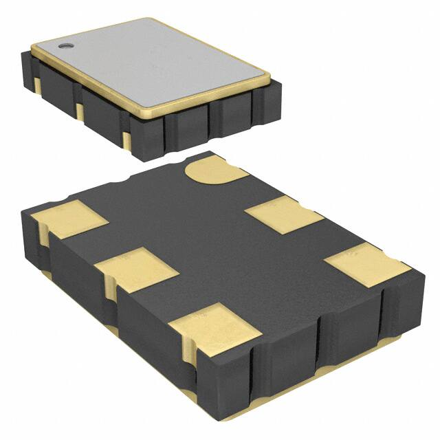
Si51218 Data Sheet
Three Output Factory Programmable Clock Generator
KEY FEATURES
The factory programmable Si51218 is a low power, small footprint and frequency flexible
programmable clock generator targeting low power, low cost and high volume consumer
and embedded applications. The device operates from a single crystal or an external
clock source and generates up to 3 outputs from 32.768 kHz to 170 MHz. The device is
factory programmed to provide customized output frequencies and control input such as
power down and output enable.
Applications
XOUT 2
VDDO 8
VDD 1
VSS 5
1
To Pin 6/7
V-REG
To Core
To Pin 4
Programmable
Configuration
Register
• 8 to 48 MHz crystal input
4
PLL with
Modulation
Control
XIN/
3
CLKIN
• Accepts crystal or reference clock input
• 3 to 165 MHz reference clock input
• Programmable OE input function
• Portable devices
• DTV/IPTV
• Crystal/XO replacement
• Digital media players
• Generates up to 3 LVCMOS clock outputs
from 32.768 kHz to 170 MHz
Buffers,
Dividers,
and
Switch
Matrix
6
CLKOUT1/REFOUT1
(VDD)/OE
CLKOUT2/REFOUT2
(VDDO)/
OE
7 CLKOUT3 (VDDO)
Skyworks Solutions, Inc. • Phone [781] 376-3000 • Fax [781] 376-3100 • sales@skyworksinc.com • www.skyworksinc.com
Rev. 1.1 • Skyworks Proprietary Information • Products and Product Information are Subject to Change Without Notice • December 1, 2021
1
�Table of Contents
1. Feature List . . . . . . . . . . . . . . . . . . . . . . . . . . . . . . . . 3
2. Design Considerations. . . . . . . . . . . . . . . . . . . . . . . . . . . . 4
2.1 Typical Application Schematic .
.
.
.
.
.
.
.
.
.
.
.
.
.
.
.
.
.
.
.
.
.
.
.
. 4
2.2 Comments and Recommendations .
.
.
.
.
.
.
.
.
.
.
.
.
.
.
.
.
.
.
.
.
.
. 4
3. Electrical Specifications . . . . . . . . . . . . . . . . . . . . . . . . . . . 5
4. Functional Description. . . . . . . . . . . . . . . . . . . . . . . . . . . . 8
4.1 Input Frequency Range .
.
.
.
.
.
.
.
.
.
.
.
.
.
.
.
.
.
.
.
.
.
. 8
4.2 Output Frequency Range and Outputs .
.
.
.
.
.
.
.
.
.
.
.
.
.
.
.
.
.
.
.
.
. 8
4.3 Output Enable (OE) .
.
.
.
.
.
.
.
.
.
.
.
.
.
.
.
.
.
.
.
.
. 8
.
.
.
.
.
.
.
.
.
.
5. Pin Description
. . . . . . . . . . . . . . . . . . . . . . . . . . . . . . 9
6. Ordering Guide
. . . . . . . . . . . . . . . . . . . . . . . . . . . . .
10
7. Package Outline . . . . . . . . . . . . . . . . . . . . . . . . . . . . . .11
8. PCB Land Pattern
. . . . . . . . . . . . . . . . . . . . . . . . . . . .
13
9. Revision History . . . . . . . . . . . . . . . . . . . . . . . . . . . . .
14
Skyworks Solutions, Inc. • Phone [781] 376-3000 • Fax [781] 376-3100 • sales@skyworksinc.com • www.skyworksinc.com
Rev. 1.1 • Skyworks Proprietary Information • Products and Product Information are Subject to Change Without Notice • December 1, 2021
2
2
�Si51218 Data Sheet • Feature List
1. Feature List
The Si51218 highlighted features are listed below.
• Generates up to 3 LVCMOS clock outputs from 32.768 kHz to
170 MHz
• Accepts crystal or reference clock input
• 3 to 165 MHz reference clock input
• 8 to 48 MHz crystal input
• Programmable OE input function
• Low power dissipation
3
• Separate voltage supply pins
• VDD = 2.5 to 3.3 V
• VDDO = 1.8 to 3.3 V (VDDO < VDD)
• Low cycle-cycle jitter
• Ultra small 8-pin TDFN package (1.4 mm x 1.6 mm)
Skyworks Solutions, Inc. • Phone [781] 376-3000 • Fax [781] 376-3100 • sales@skyworksinc.com • www.skyworksinc.com
Rev. 1.1 • Skyworks Proprietary Information • Products and Product Information are Subject to Change Without Notice • December 1, 2021
3
�Si51218 Data Sheet • Design Considerations
2. Design Considerations
2.1 Typical Application Schematic
2.2 Comments and Recommendations
Decoupling Capacitor: A decoupling capacitor of 0.1 μF must be used between VDD and VSS on pins 1 and 8. Place the capacitor
on the component side of the PCB as close to the VDD pin as possible. The PCB trace to the VDD pin and to the GND via should be
kept as short as possible. Do not use vias between the decoupling capacitor and the VDD pin. In addition, a 10 µF capacitor should be
placed between VDD and VSS.
Crystal and Crystal Load: Only use a parallel resonant fundamental AT cut crystal. Do not use higher overtone crystals. To meet
the crystal initial accuracy specification (in ppm) make sure that the external crystal load capacitor is matched to the crystal load
specification. To determine the value of CL1 and CL2, use the following formula:
CL1 = CL2 = 2CL − Cpin + Cp ;
where CL is the load capacitance stated by the crystal manufacturer,
Cpin is the Si51218 pin capacitance (3 pF), and
Cp is the parasitic capacitance of the PCB traces.
Example: If a crystal with CL = 12 pF specification is used and Cp = 1 pF (parasitic PCB capacitance on PCB), 19 pF external
capacitors from pins XIN (pin 3) and XOUT (Pin 2) to VSS are required. Users must verify Cp value.
Table 2.1. Crystal Specifications
4
Equivalent Series Resistance (ESR)
Crystal Output Capacitance (CO)
Load Capacitance (CL)
< 50 Ω
< 3 pF
< 13 pF
Skyworks Solutions, Inc. • Phone [781] 376-3000 • Fax [781] 376-3100 • sales@skyworksinc.com • www.skyworksinc.com
Rev. 1.1 • Skyworks Proprietary Information • Products and Product Information are Subject to Change Without Notice • December 1, 2021
4
�Si51218 Data Sheet • Electrical Specifications
3. Electrical Specifications
Table 3.1. DC Electrical Specifications
(VDD = 2.5 V ±10%, or VDD = 3.3V ±-10%, VDDO = VDD, CL = 10 pF, TA = –40 to 85 °C)
Parameter
Operating Voltage
Output High Voltage
Symbol
Test Condition
Min
Typ
Max
Unit
VDD
VDD= 3.3 V ± 10%
2.97
3.3
3.63
V
VDD= 2.5 V ± 10%
2.25
2.5
2.75
V
VDDO
VDDO < VDD
1.71
—
3.6
V
VOH
IOH= –4 mA
VDDX –
0.5
—
—
V
VDDX = VDD or VDDO
Output Low Voltage
VOL
IOL= 4 mA
—
—
0.3
V
Input High Voltage
VIH
CMOS Level
0.7 VDD
—
—
V
Input Low Voltage
VIL
CMOS Level
—
—
0.3 VDD
V
Operating Supply Current1
IDD
FIN = 20 MHz, CLKOUT1 =
32.768 kHz, REFOUT2 = 20 MHz,
CLKOUT3 = 26 MHz, CL= 5 pF,
VDD = VDDO = 3.3 V
—
7.6
9
mA
Nominal Output Impedance
ZO
—
30
—
Ω
Internal Pull-up/Pull-down Resistor
RPUP/RPD
Pin 6
—
150k
—
Ω
Input Pin Capacitance
CIN
Input pin capacitance
—
3
5
pF
Load Capacitance
CL
—
—
10
pF
Note:
1. IDD depends on input and output frequency configurations.
Table 3.2. AC Electrical Specifications
(VDD = 2.5 V ±10%, or VDD = 3.3 V ±10%, VDDO = VDD, CL = 10 pF, TA = –40 to 85 °C)
Parameter
Symbol
Condition
Min
Typ
Max
Unit
Input Frequency Range
FIN1
Crystal input
8
—
48
MHz
Input Frequency Range
FIN2
Reference clock Input
3
—
165
MHz
Output Frequency Range
FOUT
—
170
MHz
Frequency Accuracy
FACC
Configuration dependent
—
0
—
ppm
DCOUT
Measured at VDDO/2
45
50
55
%
40
50
60
%
Output Duty Cycle
CLKOUT1: 32.768 kHz to 170 MHz 0.032768
CLKOUT2/3: 3 MHz to 170 MHz
FOUT < 75 MHz
Measured at VDDO/2
FOUT > 75 MHz
5
Skyworks Solutions, Inc. • Phone [781] 376-3000 • Fax [781] 376-3100 • sales@skyworksinc.com • www.skyworksinc.com
Rev. 1.1 • Skyworks Proprietary Information • Products and Product Information are Subject to Change Without Notice • December 1, 2021
5
�Si51218 Data Sheet • Electrical Specifications
Parameter
Symbol
Condition
Min
Typ
Max
Unit
DCIN
CLKIN, CLKOUT through PLL
30
50
70
%
Output Rise/Fall Time
tr/tf
CL= 10 pF, 20 to 80%
—
1
2
ns
Period Jitter
PJ1
CLKOUT1/2/3, at the same frequency
—
12
20
ps rms
PJ2
CLKOUT1/2/3, at different output
frequencies1
—
30
952
ps rms
PJ3
CLKOUT1/3 at 32.768 kHz, VDD =
VDDO = 3.3 V
CCJ1
CLKOUT1/2/3, at the same frequency
—
85
150
ps
CCJ2
CLKOUT1/2/3, at different output
frequencies1
—
145
2902
ps
Power-up Time
tPU
Time from 0.9 VDD to valid
frequencies at all clock outputs
—
1.2
5
ms
Output Enable Time
tOE
Time from OE rising edge to active at outputs SSCLK1/2 (asynchronous), FOUT = 133 MHz
—
15
—
ns
Output Disable Time
tOD
Time from OE falling edge to active at outputs SSCLK1/2 (asynchronous), FOUT = 133 MHz
—
15
—
ns
Min
Typ
Max
Unit
–0.5
—
4.2
V
Input Duty Cycle
Cycle-to-Cycle Jitter
ps
15002
Note:
1. Example frequency configurations:
• 8 MHz, 100 MHz, 75 MHz
• 48 MHz, 100 MHz, 66 2/3 MHz
• 96 MHz, 133 1/3 MHz, 133 1/3 MHz
2. Jitter performance depends on configuration and programming parameters.
Table 3.3. Absolute Maximum Conditions
Parameter
Symbol
Main Supply Voltage
VDD_3.3V
Condition
Input Voltage
VIN
Relative to VSS
–0.5
—
VDD+0.5
V
Temperature, Storage
TS
Non-functional
–65
—
150
°C
Temperature, Operating Ambient
TA
Functional, I-Grade
–40
—
85
°C
Temperature, Junction
TJ
Functional, power is applied
—
—
125
°C
Temperature, Soldering
TSol
Non-functional
—
—
260
°C
ESD Protection (Human Body Model)
ESDHBM
JEDEC (JESD 22-A114)
–4000
—
4000
V
ESD Protection (Charge Device
Model)
ESDCDM
JEDEC (JESD 22-C101)
–1500
—
1500
V
ESD Protection (Machine Model)
ESDMM
JEDEC (JESD 22-A115)
–200
—
200
V
6
Skyworks Solutions, Inc. • Phone [781] 376-3000 • Fax [781] 376-3100 • sales@skyworksinc.com • www.skyworksinc.com
Rev. 1.1 • Skyworks Proprietary Information • Products and Product Information are Subject to Change Without Notice • December 1, 2021
6
�Si51218 Data Sheet • Electrical Specifications
Parameter
Symbol
Condition
Min
Typ
Max
Unit
Note:
1. While using multiple power supplies, the voltage on any input or I/O pin cannot exceed the power pin during power-up. Power
supply sequencing is not required.
Table 3.4. Thermal Characteristics
Parameter
Symbol
Condition
Value
Unit
Thermal Resistance Junction to Ambient
θJA
Still air
170.8
°C/W
Thermal Resistance Junction to Case
θJC
Still air
VDD+0.5
°C/W
7
Skyworks Solutions, Inc. • Phone [781] 376-3000 • Fax [781] 376-3100 • sales@skyworksinc.com • www.skyworksinc.com
Rev. 1.1 • Skyworks Proprietary Information • Products and Product Information are Subject to Change Without Notice • December 1, 2021
7
�Si51218 Data Sheet • Functional Description
4. Functional Description
4.1 Input Frequency Range
The input frequency range is from 8.0 to 48.0 MHz for crystals and ceramic resonators. If an external clock is used, the input frequency
range is from 3.0 to 165.0 MHz.
4.2 Output Frequency Range and Outputs
Up to three outputs can be programmed as CLKOUT or REFOUT. The CLKOUT1 synthesized frequencies can have values from
32.768 kHz to 170 MHz. REFOUT is the buffered output of the oscillator and is the same frequency as the input frequency. By using
only low cost, fundamental mode crystals, the Si51218 can synthesize output frequencies up to 170 MHz (CLKOUT2/3), eliminating the
need for higher order crystals (Xtals) and crystal oscillators (XOs). The 32.768 kHz output can replace the 32.768 kHz crystal, which is
widely used in many embedded and mobile systems. This reduces the cost while improving the system clock accuracy, performance,
and reliability.
4.3 Output Enable (OE)
The Si51218 pin 4 and pin 6 can be programmed as OE input. OE only disables the output buffers to Hi-Z. The OE function is
asynchronous. Any requirement for synchronous operations (like glitchless output clock switching) needs to be handled externally.
8
Skyworks Solutions, Inc. • Phone [781] 376-3000 • Fax [781] 376-3100 • sales@skyworksinc.com • www.skyworksinc.com
Rev. 1.1 • Skyworks Proprietary Information • Products and Product Information are Subject to Change Without Notice • December 1, 2021
8
�Si51218 Data Sheet • Pin Description
5. Pin Description
VDD
1
XOUT
2
XIN/CLKIN
CLKOUT1/
REFOUT1/OE
8
VDDO
7
CLKOUT3
3
6
CLKOUT2/REFOUT2/
OE
4
5
VSS
Si51218
Figure 5.1. 8-Pin TDFN
Table 5.1. Si51218 8-Pin Descriptions
9
Pin #
Name
Type
Description
1
VDD
PWR
2.5 to 3.3 V power supply.
2
XOUT
O
Crystal output. Leave this pin unconnected (floating) if an external
clock input is used.
3
XIN/CLKIN
I
External crystal and clock input.
4
CLKOUT1/REFOUT1/OE
I/O
5
VSS
GND
6
CLKOUT2/REFOUT2/OE
I/O
Programmable CLKOUT2 or REFOUT2 output or OE control input. The frequency at this pin is synthesized by the internal PLL
if programmed as CLKOUT2. This output clock can also be the
buffered output (REFOUT2) of the crystal or reference clock input.
It is powered by the VDDO pin (pin 8).
7
CLKOUT3
O
Programmable CLKOUT3 output. The frequency at this pin is synthesized by the internal PLL. It is powered by the VDDO pin (pin 8).
8
VDDO
PWR
Programmable CLKOUT1 or REFOUT1 output or OE control input. The frequency at this pin is synthesized by the internal PLL
if programmed as CLKOUT1. If programmed as REFOUT1, the
output clock is a buffered output of the crystal or reference clock
input.
Ground.
1.8 to 3.3 V output power supply to CLKOUT2/3 (pin 6/7).
Skyworks Solutions, Inc. • Phone [781] 376-3000 • Fax [781] 376-3100 • sales@skyworksinc.com • www.skyworksinc.com
Rev. 1.1 • Skyworks Proprietary Information • Products and Product Information are Subject to Change Without Notice • December 1, 2021
9
�Si51218 Data Sheet • Ordering Guide
6. Ordering Guide
Table 6.1. Si51218 Ordering Guide
Part Number
Package Type
Temperature
Si51218-Axxxxx-GM
8-pin TDFN
Industrial, –40 to 85 °C
Si51218-Axxxxx-GMR
8-pin TDFN—Tape and Reel
Industrial, –40 to 85 °C
Si51218
Si 52112
Base part number
Axxxxx
Bx
GMR
GM2R
G = -40 to 85°C (Operating temp
range)
M = TDFN, ROHS6, Pb free
R = Tape & Reel; (Blank) = Coil Tape
A = Product Revision A
xxxxx = 2nd option code
A five character code will be assigned
for each unique configuration
10
Skyworks Solutions, Inc. • Phone [781] 376-3000 • Fax [781] 376-3100 • sales@skyworksinc.com • www.skyworksinc.com
Rev. 1.1 • Skyworks Proprietary Information • Products and Product Information are Subject to Change Without Notice • December 1, 2021
10
�Si51218 Data Sheet • Package Outline
7. Package Outline
Figure 7.1. 8-pin TDFN
Table 7.1. Si51218 Package Dimensions
Dimension
Min
Nom
Max
A
0.70
0.75
0.80
A1
0.00
0.02
0.05
A3
b
0.20 REF
0.15
D
D2
11
0.20
0.25
1.60 BSC
1.00
1.05
e
0.40 BSC
E
1.40 BSC
1.10
E2
0.20
0.25
0.30
L
0.30
0.35
0.40
aaa
0.10
bbb
0.10
ccc
0.10
ddd
0.07
eee
0.08
Skyworks Solutions, Inc. • Phone [781] 376-3000 • Fax [781] 376-3100 • sales@skyworksinc.com • www.skyworksinc.com
Rev. 1.1 • Skyworks Proprietary Information • Products and Product Information are Subject to Change Without Notice • December 1, 2021
11
�Si51218 Data Sheet • Package Outline
Dimension
Min
Nom
Max
Note:
1. All dimensions shown are in millimeters (mm) unless otherwise noted..
2. Dimensioning and Tolerancing per ANSI Y14.5M-1994.
3. Recommended card reflow profile is per the JEDEC/IPC J-STD-020 specification for Small Body Components.
12
Skyworks Solutions, Inc. • Phone [781] 376-3000 • Fax [781] 376-3100 • sales@skyworksinc.com • www.skyworksinc.com
Rev. 1.1 • Skyworks Proprietary Information • Products and Product Information are Subject to Change Without Notice • December 1, 2021
12
�Si51218 Data Sheet • PCB Land Pattern
8. PCB Land Pattern
The figure below illustrates the PCB land pattern details for the device. The table below lists the values for the dimensions shown in the
illustration.
Figure 8.1. Si51218 8-pin TDFN PCB Land Pattern
Table 8.1. PCB Land Pattern Dimensions
13
Dimension
mm
C
1.40
E
0.40
X1
0.75
Y1
0.20
X2
0.25
Y2
1.10
Skyworks Solutions, Inc. • Phone [781] 376-3000 • Fax [781] 376-3100 • sales@skyworksinc.com • www.skyworksinc.com
Rev. 1.1 • Skyworks Proprietary Information • Products and Product Information are Subject to Change Without Notice • December 1, 2021
13
�Si51218 Data Sheet • Revision History
9. Revision History
Revision 1.1
• Updated key features.
• Updated block diagram.
• Updated 2. Design Considerations.
• Updated 3. Electrical Specifications.
• Updated 6. Ordering Guide.
Revision 1.0
• Updated max output frequency to 170 MHz.
• Updated max clock input frequency to 165 MHz.
• Updated Operating Temperature to Industrial temperature, –40 °C to 85 °C.
• Removed programmable output rise/fall time.
• Updated Table 3.1 DC Electrical Specifications on page 5.
• Updated Table 3.2 AC Electrical Specifications on page 5.
• Updated pin descriptions in Pin Descriptions table.
• Updated customized part numbering nomenclature in 6. Ordering Guide.
• Added land pattern drawing.
• Removed FSEL and PD functions.
14
Skyworks Solutions, Inc. • Phone [781] 376-3000 • Fax [781] 376-3100 • sales@skyworksinc.com • www.skyworksinc.com
Rev. 1.1 • Skyworks Proprietary Information • Products and Product Information are Subject to Change Without Notice • December 1, 2021
14
�ClockBuilder Pro
Customize Skyworks clock generators,
jitter attenuators and network
synchronizers with a single tool. With
CBPro you can control evaluation
boards, access documentation, request
a custom part number, export for
in-system programming and more!
www.skyworksinc.com/CBPro
Portfolio
SW/HW
Quality
Support & Resources
www.skyworksinc.com/ia/timing
www.skyworksinc.com/CBPro
www.skyworksinc.com/quality
www.skyworksinc.com/support
Copyright © 2021 Skyworks Solutions, Inc. All Rights Reserved.
Information in this document is provided in connection with Skyworks Solutions, Inc. (“Skyworks”) products or services. These materials, including the
information contained herein, are provided by Skyworks as a service to its customers and may be used for informational purposes only by the customer.
Skyworks assumes no responsibility for errors or omissions in these materials or the information contained herein. Skyworks may change its documentation,
products, services, specifications or product descriptions at any time, without notice. Skyworks makes no commitment to update the materials or
information and shall have no responsibility whatsoever for conflicts, incompatibilities, or other difficulties arising from any future changes.
No license, whether express, implied, by estoppel or otherwise, is granted to any intellectual property rights by this document. Skyworks assumes no liability
for any materials, products or information provided hereunder, including the sale, distribution, reproduction or use of Skyworks products, information or
materials, except as may be provided in Skyworks’ Terms and Conditions of Sale.
THE MATERIALS, PRODUCTS AND INFORMATION ARE PROVIDED “AS IS” WITHOUT WARRANTY OF ANY KIND, WHETHER EXPRESS, IMPLIED, STATUTORY, OR
OTHERWISE, INCLUDING FITNESS FOR A PARTICULAR PURPOSE OR USE, MERCHANTABILITY, PERFORMANCE, QUALITY OR NON-INFRINGEMENT OF ANY
INTELLECTUAL PROPERTY RIGHT; ALL SUCH WARRANTIES ARE HEREBY EXPRESSLY DISCLAIMED. SKYWORKS DOES NOT WARRANT THE ACCURACY OR
COMPLETENESS OF THE INFORMATION, TEXT, GRAPHICS OR OTHER ITEMS CONTAINED WITHIN THESE MATERIALS. SKYWORKS SHALL NOT BE LIABLE FOR
ANY DAMAGES, INCLUDING BUT NOT LIMITED TO ANY SPECIAL, INDIRECT, INCIDENTAL, STATUTORY, OR CONSEQUENTIAL DAMAGES, INCLUDING WITHOUT
LIMITATION, LOST REVENUES OR LOST PROFITS THAT MAY RESULT FROM THE USE OF THE MATERIALS OR INFORMATION, WHETHER OR NOT THE RECIPIENT
OF MATERIALS HAS BEEN ADVISED OF THE POSSIBILITY OF SUCH DAMAGE.
Skyworks products are not intended for use in medical, lifesaving or life-sustaining applications, or other equipment in which the failure of the Skyworks
products could lead to personal injury, death, physical or environmental damage. Skyworks customers using or selling Skyworks products for use in such
applications do so at their own risk and agree to fully indemnify Skyworks for any damages resulting from such improper use or sale.
Customers are responsible for their products and applications using Skyworks products, which may deviate from published specifications as a result of
design defects, errors, or operation of products outside of published parameters or design specifications. Customers should include design and operating
safeguards to minimize these and other risks. Skyworks assumes no liability for applications assistance, customer product design, or damage to any
equipment resulting from the use of Skyworks products outside of Skyworks’ published specifications or parameters.
Skyworks, the Skyworks symbol, Sky5®, SkyOne®, SkyBlue™, Skyworks Green™, Clockbuilder®, DSPLL®, ISOmodem®, ProSLIC®, and SiPHY® are trademarks or
registered trademarks of Skyworks Solutions, Inc. or its subsidiaries in the United States and other countries. Third-party brands and names are for
identification purposes only and are the property of their respective owners. Additional information, including relevant terms and conditions, posted at
www.skyworksinc.com, are incorporated by reference.
Skyworks Solutions, Inc. | Nasdaq: SWKS | sales@skyworksinc.com | www.skyworksinc.com
USA: 781-376-3000 | Asia: 886-2-2735 0399 | Europe: 33 (0)1 43548540 |
�