APX4 – WIRELESS SYSTEM-ON-MODULE
DATA SHEET
Tuesday, 23 July 2013
Version 1.01
�Copyright © 2000-2013 Bluegiga Technologies
All rights reserved.
Bluegiga Technologies assumes no responsibility for any errors which may appear in this manual.
Furthermore, Bluegiga Technologies reserves the right to alter the hardware, software, and/or specifications
detailed here at any time without notice and does not make any commitment to update the information
contained here. Bluegiga’s products are not authorized for use as critical components in life support devices
or systems.
The WRAP, Bluegiga Access Server, Access Point and iWRAP are registered trademarks of Bluegiga
Technologies.
The Bluetooth trademark is owned by the Bluetooth SIG Inc., USA and is licensed to Bluegiga Technologies.
All
other
trademarks
listed
herein
are
owned
by
their
respective
owners.
Bluegiga Technologies Oy
�VERSION HISTORY
Version
Comment
0.1
First draft
0.2
Defined screws and attachment to motherboard
0.3.1
Some small fixes and additions
0.3
TBDs defined
0.4
Review
0.4.1
Small fix to part number clarification
0.4.2
Updated document name, product description and contact information
0.4.3
Added Bluetooth RF specifications
0.5
Clarified pins etc.
0.6
Fixed layout. Removed software version from part number.
0.7
Styles updated and fixed
Added notes about missing information
0.8
Added Mouser part number for the SO-DIMM receptacle
0.9
Chapter 6.5.1 removed
1.0
Added FCC/IC texts, removed battery related texts
1.01
Typos
Bluegiga Technologies Oy
�TABLE OF CONTENTS
1
Ordering Information......................................................................................................................................7
1.1
2
3
4
APx4 pin descriptions ....................................................................................................................................8
2.1
Receptacle ............................................................................................................................................8
2.2
Power contacts on the left side .............................................................................................................8
2.3
Debug UART on the right side ..............................................................................................................8
2.4
SO-DIMM connection pin descriptions ..................................................................................................9
Power subsystem ....................................................................................................................................... 22
3.1
PSWITCH_OUT pin 14 ...................................................................................................................... 23
3.2
RESETN ............................................................................................................................................. 23
Processor subsystem ................................................................................................................................. 24
4.1
5
Bootmodes ......................................................................................................................................... 24
Wireless interfaces ..................................................................................................................................... 25
5.1
Bluetooth ............................................................................................................................................ 25
5.1.1
Bluetooth GPIOs ........................................................................................................................... 25
5.1.2
Bluetooth Audio interface .............................................................................................................. 25
5.1.3
Bluetooth PCM slots and formats.................................................................................................. 26
5.1.4
Bluetooth I2S interface .................................................................................................................. 26
5.2
6
Part number decoder .............................................................................................................................7
Wi-Fi ................................................................................................................................................... 27
Peripheral interfaces................................................................................................................................... 28
6.1
Ethernet .............................................................................................................................................. 28
6.2
USB .................................................................................................................................................... 29
6.3
I2C ...................................................................................................................................................... 29
6.4
PWM outputs ...................................................................................................................................... 30
6.5
SDIO / SPI / MMC .............................................................................................................................. 31
6.6
UARTs ................................................................................................................................................ 32
6.6.1
UART 0.......................................................................................................................................... 32
6.6.2
UART 2.......................................................................................................................................... 32
6.6.3
UART 3.......................................................................................................................................... 32
6.6.4
UART 4.......................................................................................................................................... 33
6.6.5
Debug UART ................................................................................................................................. 33
6.7
CAN .................................................................................................................................................... 34
6.8
Processor Audio ................................................................................................................................. 34
6.9
LCD .................................................................................................................................................... 35
6.10
LRADC0-6 (Touch interface) .............................................................................................................. 36
6.11
HSADC (High-Speed ADC) ................................................................................................................ 37
Bluegiga Technologies Oy
�6.12
7
JTAG .................................................................................................................................................. 37
Electrical Characteristics ............................................................................................................................ 39
7.1
Absolute Maximum Ratings................................................................................................................ 39
7.2
Recommended Operating Conditions ................................................................................................ 39
7.3
Power Consumption ........................................................................................................................... 40
8
RF Characteristics ...................................................................................................................................... 41
9
Physical Dimensions .................................................................................................................................. 43
10
Attachment to motherboard ................................................................................................................ 44
11
Layout Guidelines ............................................................................................................................... 45
11.1
Internal antenna: Optimal module placement .................................................................................... 45
11.2
External antenna ................................................................................................................................ 45
11.3
Thermal Considerations ..................................................................................................................... 45
11.4
EMC Considerations for Motherboard ................................................................................................ 45
12
Certifications ....................................................................................................................................... 47
12.1
CE....................................................................................................................................................... 47
12.2
FCC .................................................................................................................................................... 47
12.3
IC ........................................................................................................................................................ 48
12.4
IC ........................................................................................................................................................ 49
12.5
MIC, formerly TELEC ......................................................................................................................... 51
12.6
Qualified Antenna Types for APx4-E ................................................................................................. 51
13
Contact Information ............................................................................................................................ 52
Bluegiga Technologies Oy
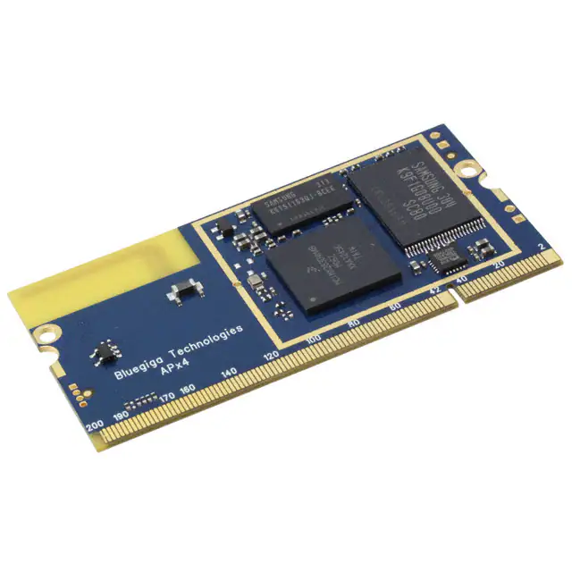
�KEY FEATURES
DESCRIPTION
The Bluegiga APx4 is a small form factor, low
power system-on-module that includes the
latest wireless connectivity standards: 802.11
b/g/n and Bluetooth 4.0. APx4 is based on
Freescale's i.MX28 processor family and runs
an embedded Linux operating system based on
TM
the Yocto Project . In addition to integrating
the 454MHz ARM9 processor, the wireless
connectivity technologies, Linux operating
system the APx4 also includes with several built
in applications, such as the 802.11
and Bluetooth 4.0 stacks,
Continua
v.1.5 compliant IEEE manager and many more.
This combination provides an ideal platform for
designing multi-radio wireless gateways that
enables fast time-to-market and minimum R&D
risks.
The Bluegiga APx4 software can be easily
extended or tailored customizing the Linux
operating system with applications. The
motherboards for the APx4 can be easily
extended to include almost anything from 3G
modems to Ethernet and audio interfaces to
and touch screen displays.
The Bluegiga APx4 is an ideal product for
applications requiring wireless or wired
connectivity technologies and the processing
power of the ARM9 processor, such as health
and fitness gateways, building and home
automation gateways, M2M, point-of-sale and
industrial connectivity.
454MHz ARM9 core (Freescale
i.MX28)
64MB RAM
128MB Flash
Real Time Clock
Linux operating system
SO-DIMM form factor
A connectivity platform:
Bluetooth 4.0 dual-mode radio
2.4GHz 802.11 b/g/n radio
Wi-Fi Access Point mode
10/100 Ethernet
USB 2.0 High Speed
With many extension options:
Up to 800 x 480, 24bit display
Resistive touch screen
MMC/SDIO
Multiple SPI, UART and I²C
I²S
PWM, GPIO and AIO
Linux operating system:
Based on the Yocto Project(TM)
Thousands of open source software
packets available
Qualifications:
APPLICATIONS:
APx4 is a computing platform:
Health gateways
M2M connectivity
Fitness gateways
Home and building automation
Point-of-sale gateways
People and asset tracking
Bluetooth
CE
FCC and IC
Figure 1: Physical outlook
Bluegiga Technologies Oy
�1
Ordering Information
Product code
CPU and memories
Connectivity
Antenna
Temperature
range
APX4-367CC-A
i.MX283
Bluetooth + Wi-Fi
Internal
antenna
-10 – 50°C
64MB DDR2
128MB Flash
1.1 Part number decoder
APX 4 – 3 6 7 C C – A
Product category
APX
Product generation
4
Processor
3: i.MX283
Memory
6: 64MB
Flash
7: 128MB
Connectivity
C: Bluetooth and Wi-Fi
Temperature
C: Commercial
I: Industrial (contact sales@bluegiga.com)
Antenna
A: Internal antenna
E: External antenna
Note: Not all variants are available. Minimum order quantities and lead times may apply for special variants.
Please contact Bluegiga Technologies Oy for more information.
Bluegiga Technologies Oy
Page 7 of 52
�2
APx4 pin descriptions
The APX4 connector uses a standard DDR1 SO-DIMM connector with 2.5V keying.
Odd numbered pins are located on top layer
Even numbered pins are located on bottom layer
There is a ½ pitch (0.3mm) offset from top layer pins to bottom layer pins.
Note that most receptacles also have 0.3mm offset from odd pins to even pins.
2.1 Receptacle
Suitable receptacles are available from multiple vendors. For example TE Connectivity’s part number
1473005-1, Mouser part number: 571-1473005-1 and Digi-Key’s part number: A99605-ND.
PCB footprint and schematic symbol for the mentioned part number will be available for download
from Techforum in Mentor Graphics’ PADS format.
2.2 Power contacts on the left side
In addition to the 200 pins/finger contacts there are two pairs of plated through holes on the left side of the
module which can be used for powering the module stand-alone (not assembled on any motherboard). The
pitch between the holes is 2.54mm. Leave the holes unconnected if the module is assembled on a
motherboard.
Name
Function
GND
Ground
VIN
+5V input
GND
Ground
VBATTERY
Battery positive input/output
Table 1: Power supply pins
2.3 Debug UART on the right side
On the right side there are four plated through holes for PWM or debug port stand-alone (not assembled on
any motherboard). The vertical distance between the holes is 1.27mm:
Name
Function
3V3
3.3V output (for current limits, see Table 50)
PWM1/DUART TxD
Debug UART data transmit, logic level 3.3V
PWM0/DUART RxD
Debug UART data receive, logic level 3.3V
GND
Ground
Table 2: Debug UART pins
Bluegiga Technologies Oy
Page 8 of 52
�2.4 SO-DIMM connection pin descriptions
Note: Signals/nets marked with a star (*) are not present on standard version
Pin#
Default function
Net name
Note
1
5V input
VIN
2
5V input
VIN
3
5V input
VIN
4
5V input
VIN
5
Battery input/output
VBATTERY
6
Battery input/output
VBATTERY
7
Battery input/output
VBATTERY
8
Bootmode
BOOTMODE
9
3.3V output
3V3
Pins 9-10 may source up to
200mA combined.
10
3.3V output
3V3
Pins 9-10 may source up to
200mA combined.
11
3.3V output
3V3
Pins 9-10 may source up to
200mA combined.
12
3.3V output
3V3
Pins 9-10 may source up to
200mA combined.
13
RTC battery
VBACKUP
14
PS switch
PSWITCH_OUT
15
NC
NC
16
NC
NC
17
Reset in - Master reset
RESETN
18
Ground
GND
Table 3: Main power pins
Bluegiga Technologies Oy
Page 9 of 52
�Pin#
Default function
Net name
19
Ethernet TX -
ETN_TXN
20
GND
GND
21
Ethernet TX +
ETN_TXP
22
3.3V output
3V3
23
Ethernet RX -
ETN_RXN
24
Ethernet LED
ETN_LED1N*
25
Ethernet RX +
ETN_RXP
26
GND
GND
Table 4: Ethernet
* See 6.1 for detailed function.
Pin#
Default function
Net name
27
USB External VBUS enable
SPDIF*
28
29
NC
USB D-
30
USB1DM
NC
31
USB D+
USB1DP
32
Ground
GND
Table 5: USB Host
Bluegiga Technologies Oy
Page 10 of 52
�Pin#
Default function
Net name
33
USB OTG id
USB0_ID
34
35
NC
USB D-
USB0DM
36
37
NC
USB D+
USB0DP
38
39
NC
Ground
GND
Table 6: USB On-the-go
Pin#
Default function
40
I C Data
41
I C Clock
Net name
2
I2C0_SDA
2
I2C0_SCL
2
Table 7: I C 0
Pin#
Default function
Net name
42
PWM (Backlight)
PWM4
43
Status led
PWM3
Table 8: Dedicated PWMs
Bluegiga Technologies Oy
Page 11 of 52
�Pin#
Default function
Net name
44
Slave select 1
SDIO_DAT1_OUT*
45
Slave select 2
SDIO_DAT2_OUT*
46
Command - Master out, slave in
SDIO_CMD_OUT*
47
Data 0, Master in, slave out
SDIO_DAT0_OUT*
48
Clock
SDIO_CLK_OUT*
49
Ready - Slave select 0
SDIO_DAT3_OUT*
50
Ground
GND
Table 9: SSP2 – SDIO/MMC/SPI
Pin#
Default function
Net name
51
Card detect
SSP0_DETECT
52
Data 0
SSP0_DATA0
53
Data 1
SSP0_DATA1
54
Data 2
SSP0_DATA2
55
Data 3
SSP0_DATA3
56
Command
SSP0_CMD
57
Clock
SSP0_SCK
58
Ground
GND
Table 10: SSP0 – SDIO/MMC/SPI
Pin#
Default function
Net name
59
UART transmit
AUART0_TX
60
UART receive
AUART0_RX
61
UART clear-to-send
AUART0_CTS
62
UART request-to-send
AUART0_RTS
Table 11: UART 0
Bluegiga Technologies Oy
Page 12 of 52
�Pin#
Default function
Net name
63
UART transmit
SSP2_MOSI
64
UART receive
SSP2_SCK
65
NC
66
NC
Table 12: UART 2
Pin#
Default function
Net name
67
UART transmit
SSP2_SS0
68
UART receive
SSP2_MISO
69
NC
70
NC
71
Ground
GND
Table 13: UART 3
Pin#
Default function
Net name
72
Bluetooth GPIO
BT_PIO7
73
Bluetooth GPIO
BT_PIO8
74
Bluetooth GPIO
BT_PIO9
75
Bluetooth GPIO
BT_PIO25
Table 14: Bluetooth GPIO
Bluegiga Technologies Oy
Page 13 of 52
�Pin#
Default function
Net name
76
CAN 0 transmit
GPMI_RDY2*
77
Ground
GND
78
CAN 1 transmit
GPMI_CE2N*
79
CAN 1 receive
GPMI_CE3*
80
Ground
GND
81
CAN 0 receive
GPMI_RDY3*
82
Ground
GND
Table 15: CAN
Pin#
Default function
Net name
83
MCLK
SAIF0_MCLK
84
Data line 1
SAIF1_SDATA0
85
Data line 0
SAIF0_SDATA0
86
Bit clock
SAIF0_BITCLK
87
Left/Right clock
SAIF0_LRCLK
88
GND
GND
Table 16: Primary audio / UART 4
Bluegiga Technologies Oy
Page 14 of 52
�Pin#
Default function
Net name
89
NC
90
NC
91
NC
92
NC
93
NC
94
Ground
GND
95
NC
96
NC
97
NC
98
NC
99
NC
100
NC
Table 17: Reserved group 1
Bluegiga Technologies Oy
Page 15 of 52
�Pin#
Default function
101
102
Net name
NC
Ground
GND
103
NC
104
NC
105
NC
106
NC
107
1.4V output*
1V4_CPU
108
1.8V output*
1V8
109
4.2V output*
4V2_CPU
110
NC
111
GND
112
NC
113
NC
114
NC
115
NC
116
Ground
GND
Table 18: Reserved group 2
*Important: Pins 107-109 are only meant for manufacturing test. Please leave unconnected. Do not pull any
current from these outputs. Doing so may create a black hole in the universe.
Bluegiga Technologies Oy
Page 16 of 52
�Pin#
Default function
Net name
117
Data 0
LCD_D0
118
Data 1
LCD_D1
119
Data 2
LCD_D2
120
Data 3
LCD_D3
121
Data 4
LCD_D4
122
Data 5
LCD_D5
123
Data 6
LCD_D6
124
Data 7
LCD_D7
125
Data 8
LCD_D8
126
Data 9
LCD_D9
127
Data 10
LCD_D10
128
Data 11
LCD_D11
129
Ground
GND
130
Data 12
LCD_D12
131
Data 13
LCD_D13
132
Data 14
LCD_D14
133
Data 15
LCD_D15
134
Data 16
LCD_D16
135
Data 17
LCD_D17
136
Data 18
LCD_D18
137
Data 19
LCD_D19
138
Data 20
LCD_D20
139
Data 21
LCD_D21
140
Data 22
LCD_D22
141
Data 23
LCD_D23
142
Ground
GND
Bluegiga Technologies Oy
Page 17 of 52
�Table 19 LCD data lines
Pin#
Default function
Net name
143
Horizontal Sync
LCD_WR_RWN
144
Vertical Sync
LCD_RD_E
145
LCD Enable
LCD_CS
146
Dot clock
LCD_RS
147
Ground
GND
Table 20: LCD control lines
Pin#
Function
Net name
148
Debug UART RX or I2C1_SDA
PWM0 (also connected to PTH pins on right
side)
149
Debug UART TX or I2C1_SCL
PWM1 (also connected to PTH pins on right
side)
150
LCD reset / GPIO
LCD_RESET
151
NC
Table 21: Debug UART / PWM / I2C1 / GPIO
Bluegiga Technologies Oy
Page 18 of 52
�Pin#
Function
Net name
152
NC
153
NC
154
NC
155
NC
156
NC
157
NC
158
NC
159
Ground
GND
160
Ground
GND
161
NC
162
NC
163
Ground
GND
164
Ground
GND
165
NC
166
NC
167
Ground
GND
168
Ground
GND
169
NC
170
WiFi Activity
WIFI_ACT
171
Ground
GND
Table 22: Reserved group 3
Bluegiga Technologies Oy
Page 19 of 52
�Pin#
Function
Net name
172
Wi-Fi Debug SPI - MISO
SPI_WIFI_MISO
173
Wi-Fi Debug SPI – CLK
SPI_WIFI_CLK
174
Wi-Fi Debug SPI – MOSI
SPI_WIFI_MOSI
175
Wi-Fi Debug SPI - CS
SPI_WIFI_CS
176
RTC interrupt
INT_EXT_RTC_N
177
Factory reset button / JTAG return clock
JTAG_RTCK
178
JTAG test clock
JTAG_TCK
179
JTAG test data in
JTAG_TDI
180
JTAG test data out
JTAG_TDO
181
JTAG test mode state
JTAG_TMS
182
JTAG test reset
JTAG_TRST
183
Ground
GND
184
JTAG enable boundary scan
DEBUG
Table 23: Misc
Pin#
Function
Net name
185
Touch controller XN
LRADC4
186
Touch controller XP
LRADC2
187
Touch controller YN
LRADC5
188
Touch controller YP
LRADC3
189
Touch controller WIPER
LRADC6
190
Generic ADC 0
LRADC0
191
Generic ADC 1
LRADC1
192
High speed ADC
HSADC0
193
Ground
GND
194
Ground
GND
Table 24: ADC
Bluegiga Technologies Oy
Page 20 of 52
�Pin #
Function
Net name
195
Bluetooth debug enable
BT_SPI_PCM1N
196
PCM in
BT_PCM1_IN
197
PCM out
BT_PCM1_OUT
198
PCM clock
BT_PCM1_CLK
199
PCM sync
BT_PCM1_SYNC
200
Ground
GND
Table 25: Bluetooth audio
Bluegiga Technologies Oy
Page 21 of 52
�3
Power subsystem
Pin#
Function
APx4 net name
Description
1-4
5V input
VIN
Main power input
5-7
Battery input/output
VBATTERY
A rechargeable
connected
9-12,
22
3.3V output
3V3
For maximum current draw, see Table
50
13
RTC battery
VBACKUP
RTC battery backup power
14
Power switch
PSWITCH_OUT
Power switch
17
Reset in - Master reset
RESETN
Active low master reset. Resets the
entire board.
battery
can
be
Table 26: Power supply pins
The module is powered through the 5V input. It is recommended that all the pins (1-4) are connected together
on the application board.
The external battery connectable to VBATTERY is currently not supported.
VBACKUP is connected to the Real-Time clock battery and the VDD input of the Real Time Clock. This pin
can be used to power the real time clock in cases where the battery is not placed on the module.
3V3
Pin 13:VBACKUP
VDD
Real Time Clock
On-board
battery
Figure 2: VBACKUP and battery connection
Bluegiga Technologies Oy
Page 22 of 52
�3.1 PSWITCH_OUT pin 14
Note: In most cases the user can ignore the PSWITCH pin. Leave unconnected for normal operation.
The ÅSWITCH_OUT (pin 14) has three levels: low, mid and high. A 10kΩ pull-up to mid-level is applied on the
module to the PSWITCH line, causing the device to start booting immediately once power is applied. Boot-up
requires a mid-level voltage to be present for >100ms.
If the PSWITCH is pulled high for over 5 seconds, for example by connecting it to 3.3V, a special Freescale
USB recovery mode is entered. For further details about the power switch, refer to Freescale’s Reference
Manual, Section 11.4. This mode can also be entered using the BOOTMODE pin.
3.2 RESETN
Power-on reset is generated internally. If a reset from external pins is required use the RESETN pin. RESETN
is internally pulled up to 3.3V.
The RESETN pin must be kept low for at least 100ms and then released in order to guarantee a proper reset.
100ms
NRESET
Figure 3: NRESET
Bluegiga Technologies Oy
Page 23 of 52
�4
Processor subsystem
The processor belongs to the Freescale i.MX28-family and integrates an ARM9 core operating at 454MHz.
The standard APX4 variant uses the i.MX283 processor. The module also has 128MB of SLC NAND flash and
64MB of DDR2-400 memory. For more details regarding the features the processor offers, please see the
Freescale Reference Manual.
By default the module boots from the NAND flash into the U-Boot boot loader environment. From there the
boot loader loads a Linux kernel which boots into the Bluegiga Linux userspace.
4.1 Bootmodes
The module supports booting from multiple different media including NAND Flash, Secure Digital (SD) cards,
2
MMC cards, I C EEPROM and USB (in a device mode). The selected boot media can be selected using the
LCD_DATA[0-3] signals or in the case of USB recovery boot, by tying the BOOTMODE pin to ground.
By default the module boots from internal NAND flash, meaning that LCD_DATA[3], LCD_DATA[1] and
LCD_DATA[0] have pull-downs on the module and LCD_DATA[2] has a pull-up.
Default boot mode in bold face. The module has pull-ups and pull-downs so that when
LCD_DATA[0]..LCD_DATA[3] are left unconnected the module boots from internal NAND. After boot the
LCD_DATA lines can be used fro any purpose.
LCD_DATA[3]
LCD_DATA[2]
LCD_DATA[1]
LCD_DATA[0]
Port
0
0
0
0
USB0 device mode boot
0
0
0
1
EEPROM connected to I2C0
0
0
1
0
SPI flash on SSP2 (non-Wi-Fi
version only)
0
0
1
1
SPI flash on SSP3 (not available on
standard versions)
0
1
0
0
Module’s internal NAND Flash
0
1
1
0
Wait for JTAG connection
1
0
0
0
SPI EEPROM on SSP3 (not
available on standard versions)
1
0
0
1
SD/MMC card on SSP0
1
0
1
0
SD/MMC on SSP1 (not available on
standard versions)
Table 27: Bootmodes
Bluegiga Technologies Oy
Page 24 of 52
�5
Wireless interfaces
The wireless connectivity on the module is implemented using two separate chips which share a 2.4GHz
antenna.
5.1 Bluetooth
The module is a fully qualified Bluetooth 4.0, Class 1, system, supporting both classical Bluetooth as well as
Bluetooth Smart (Bluetooth low energy) devices simultaneously.
5.1.1 Bluetooth GPIOs
Pin#
Function
Net name
72
Bluetooth GPIO 7
BT_PIO7
73
Bluetooth GPIO 8
BT_PIO8
74
Bluetooth GPIO 9
BT_PIO9
75
Bluetooth GPIO 25
BT_PIO25
Table 28: Bluetooth GPIO
These GPIOs are controlled by the Bluetooth baseband chip. The main processor can read and write them by
issuing special commands to the Bluetooth chip, making them suitable for use as status indicators, but not for
high speed signals. For the current status of software support, please refer to the software documentation.
Contact support if needed.
The pins are bidirectional pins with internal programmable strength pull-up or pull-down. By default they are
inputs with a weak pull-down.
5.1.2 Bluetooth Audio interface
2
Pin #
Net name
PCM function
I S function
Debug interface
195
BT_SPI_PCM1N
Select Audio: GND
Select Audio: GND
Select Debug: +3.3V
196
BT_PCM1_IN
PCM in
Serial in (SD_IN)
MOSI
197
BT_PCM1_OUT
PCM out
Serial out (SD_OUT)
MISO
198
BT_PCM1_CLK
PCM clock
Serial clock (SCK)
Clock
199
BT_PCM1_SYNC
PCM sync
Write sync (WS)
Chip select (active low)
Table 29: Bluetooth audio and debug interface
2
The Bluetooth audio functionality can be configured to work in either I S or PCM mode. In addition, the
Bluetooth chip’s debug interface is multiplexed with the audio pins.
The audio interface supports continuous transmission and reception of PCM audio data over Bluetooth.
Operation in either master or slave mode are supported and many different clock modes can be supported. A
maximum of 3 SCO audio links can be transmitted through the PCM interface at any one time.
Bluegiga Technologies Oy
Page 25 of 52
�5.1.3 Bluetooth PCM slots and formats
The module receives and transmits on any selection of the first 4 slots following each sync pulse. Slot
durations are either 8 or 16 clock cycles:
8 clock cycles for 8-bit sample formats.
16 clocks cycles for 8-bit, 13-bit or 16-bit sample formats.
The supported formats are:
13-bit linear, 16-bit linear and 8-bit μ-law or A-law sample formats.
A sample rate of 8ksamples/s.
Little or big endian bit order.
For 16-bit slots, the 3 or 8 unused bits in each slot are filled with sign extension, padded with zeros or
a programmable 3-bit audio attenuation compatible with some codecs.
There is also a compatibility mode that forces PCM_OUT to be 0. In master mode, this allows for compatibility
with some codecs which control power down by forcing PCM_SYNC to 0 while keeping PCM_CLK running.
5.1.4 Bluetooth I2S interface
2
The I S mode supports left-justified and right-justified data. The interface shares the same pins as the PCM
interface, which means each audio bus is mutually exclusive in its usage.
The digital audio interface is configured using the PSKEY_DIGITAL_AUDIO_CONFIG in the Bluetooth PS
Key configuration.
The internal representation of audio samples within CSR8811 is 16-bit and data on SD_OUT is limited to 16bit per channel.
Symbol
Parameter
Minimum
Maximum
Unit
-
SCK frequency
-
6.2
MHz
-
SCK frequency
-
96
kHz
tch
SCK high time
80
-
ns
tcl
SCK low time
80
-
ns
tssu
WS valid to SCK high setup time
20
-
ns
tsh
SCK high to WS invalid hold time
2.5
-
ns
topd
SCK low to SD_OUT valid delay time
-
20
ns
tisu
SD_IN valid to SCK high setup time
20
-
ns
tih
SCK high to SD_IN invalid hold time
2.5
-
ns
2
Table 30: I S Slave mode timing
Bluegiga Technologies Oy
Page 26 of 52
�Symbol
Parameter
Minimum
Maximum
Unit
-
SCK Frequency
-
6.2
MHz
-
WS Frequency
-
96
kHz
tspd
SCK low to WS valid delay time
-
39.27
ns
topd
SCK low to SD_OUT valid delay time
-
18.44
ns
tisu
SD_IN valid to SCK high setup time
18.44
-
ns
tih
SCK high to SD_IN invalid hold time
0
-
ns
2
Table 31: I S Master mode timing
5.2 Wi-Fi
The on board Wi-Fi is designed for IEEE 802.11b/g/n in the 2.4GHz band. Hardware encryption support for
WEP40/64, WEP104/128, TKIP, CCMP (AES), BIP and CKIP provides functionality for WPA, WPA2, IEEE
802.11i, IEEE 802.11w and CCX advanced security mechanisms.
The following modulations are supported:
All mandatory IEEE 802.11b modulations: 1, 2, 5.5, 11Mbps
All IEEE 802.11g OFDM modulations: 6, 9, 12, 18, 24, 36, 48, 54Mbps
Single stream IEEE 802.11n HT modulations MCS0-7, 20MHz, 800 and 400ns guard interval: 6.5,
7.2, 13.0, 14.4, 19.5, 21.7, 26.0, 28.9, 39.0, 43.3, 52.0, 57.8, 58.5, 65.0, 72.2Mbps
STBC (Space Time Block Coding) reception for IEEE 802.11n HT modulations MCS0-7
The receiver features direct conversion architecture. Sufficient out-of-band blocking specification at the Low
Noise Amplifier (LNA) input allows the receiver to be used in close proximity to Global System for Mobile
Communications (GSM) and Wideband Code Division Multiple Access (W-CDMA) cellular phone transmitters
without being desensitized. High-order baseband filters ensure good performance against in-band
interference.
The transmitter features a direct conversion IQ transceiver. Digital baseband transmit circuitry provides the
required spectral shaping and on-chip trims are used to reduce IQ modulator distortion. Transmitter gain can
be controlled on a per-packet basis, allowing the optimization of the transmit power as a function of
modulation scheme. The modulator supports digital predistortion to reduce non-linarites in the power amplifier.
The module supports automatic PA thermal drift compensation by measuring the transmit power through an
internal power coupler.
Bluegiga Technologies Oy
Page 27 of 52
�6
Peripheral interfaces
The module allows for several kinds of different interfaces to peripherals to be used.
6.1 Ethernet
Pin#
Function
Net name
19
Ethernet TX -
ETN_TXN
20
GND
GND
21
Ethernet TX +
ETN_TXP
22
3.3V output
3V3
23
Ethernet RX -
ETN_RXN
24
Ethernet LED
ETN_LED1N
25
Ethernet RX +
ETN_RXP
26
GND
GND
Table 32: Ethernet pins
The Ethernet I/O lines are connected on the module to a standard 10Base-T/100Base-TX physical layer
transceiver (PHY). A connector board will only need to have the magnetics as well as an RJ45 jack in order to
have fully functioning Ethernet. Multiple vendors also supply RJ45 jacks with integrated magnetics under
brand names such as MagJack and PulseJack which further simplify design. A reference schematic for such a
design is available in the APx4 reference design.
When routing the Ethernet signals, care should be taken to route the differential signals together, meaning
that for example ETN_TXN and ETN_TXP should be kept close together. The traces must also be kept short
in order to avoid EMC issues.
The Ethernet LED pin (ETN_LED1N) indicates link and activity and has a maximum output drive current of 8
mA. The ETN_LED is high when no Link is present (typically connected so that a physical LED is off), low
when a Link is present (physical LED on) and toggled on activity (physical LED is blinking).
Make sure that the driving capability of 8mA is not exceeded.
Pin state
LED
Meaning
HIGH
Off
No Link
LOW
On
Link
Toggle
Blinking
Activity
Table 33: ETN_LED1N pin
Figure 4 Typical external LED connection
Bluegiga Technologies Oy
Page 28 of 52
�6.2 USB
Pin#
Function
Net name
27
USB OTG Host External VBUS enable
SPDIF*
29
USB Host D-
USB1_DM
31
USB Host D+
USB1_DP
33
USB OTG ID
USB0_ID
35
USB OTG D-
USB0_DM
37
USB OTG D+
USB0_DP
Table 34: USB pins
The module has two USB high-speed controllers, one which supports USB Host mode only and another which
support USB On-the-Go (OTG). The USB On-the-Go controller is capable of operating as a USB Host or a
USB Device and support the OTG role negotiation via the USB OTG-ID signal. For the current software
support, please see the software documentation.
The USB D+ and D- signals can be directly connected to a USB connector, however when using a connector,
protection against electrostatic discharge (ESD) should be taken into account.
Because USB high-speed is a very high frequency digital signal (480Mbps), care must be taken to route the
D+ and D- signals as close together as possible and to have a ground plane follow them. The traces must
also be kept as short as possible.
The USB Host External VBUS enable signal is not present in the standard model, and has a fixed pull-up.
For more details refer to the i.MX28 Applications Processor Reference Manual (MCIMX28RM) chapters 31
and 32.
6.3 I2C
2
Pin#
I C function
40
I C 0 Data
41
I C 0 Clock
148
I C 1 Data
149
I C 1 Clock
Alternate Functions
Net name
2
I2C0_SDA
2
I2C0_SCL
2
PWM0, Debug UART TX
PWM0/I2C1_SDA
2
PWM1, Debug UART RX
PWM1/I2C1_SCL
2
Table 35: I C interface
2
The Inter Integrated Circuit bus (I C) is a standard two-wire interface used for communication between
peripherals and the host. The interface supports both standard speed (up to 100kbps) and as fast speed
2
(400kbps) I C connection to multiple devices with the processor acting in either master or slave mode.
Bluegiga Technologies Oy
Page 29 of 52
�2
2
The primary I C interface (I C 0, pins 40 and 41) is also connected to the module’s Real Time Clock (RTC)
chip and thus some additional restrictions for the communication apply. The processor is always the master.
2
The standard 2K pull-ups are located on APx4. Do not place additional pull-ups on I C 0.
2
2
One I C slave address (1010001X) on I C 0 is reserved for the Real Time Clock PCF8563T on the APx4:
Read: 0xA3 (10100011)
Write: 0xA2 (10100010)
2
2
The secondary I C (I C 1) is available on pins 148 and 149 and can be used freely in either master or slave
2
mode. By default it is configured to provide the Debug UART. I C 1 does not have built-in pull-ups.
2
For more details about I C, please refer to the i.MX28 Applications Processor Reference Manual, chapter 27.
6.4 PWM outputs
Pin#
Default function
PWM function
Additional function
Net name
42
LCD Backlight (PWM4)
PWM4
PWM4
43
Status led (PWM3)
PWM3
PWM3
148
Debug UART TX
PWM0
I C 1 bus data
149
Debug UART RX
PWM1
83
MCLK
PWM3
84
Data line 1
PWM7
85
Data line 0
PWM6
UART 4 TX
SAIF0_SDATA0
86
Bit clock
PWM5
UART4 RX
SAIF0_BITCLK
87
Left/Right clock
PWM4
UART4 RTS
SAIF0_LRCLK
2
PWM0/I2C1_SDA
I C 1 bus clock
2
PWM1/I2C1_SCL
UART4 CTS
SAIF0_MCLK
SAIF1_SDATA0
Table 36: PWM outputs
The module has up to seven Pulse Width Modulator outputs available. Independent output control of each
phase allows 0, 1 or high-impedance to be independently selected for the active and inactive phases.
Two dedicated PWM outputs are at pins 42 and 43, and are typically used for the LCD’s backlight and as a
status led, respectively. The same PWM outputs are available also on pins 83 and 87.
The Debug UART on pins 148 and 149 can be disabled and used for two independent PWM outputs instead.
For more details about PWM, please refer to the i.MX28 Applications Processor Reference Manual, chapter
28.
Bluegiga Technologies Oy
Page 30 of 52
�6.5 SDIO / SPI / MMC
Pin#
SDIO/SD/MMC
SPI mode
Net name
51
Card detect
52
Data 0
53
Data 1
SSP0_DATA1
54
Data 2
SSP0_DATA2
55
Data 3
Slave Select
SSP0_DATA3
56
Command
MOSI
SSP0_CMD
57
Clock
Clock
SSP0_SCK
58
Ground
SSP0_DETECT
MISO
SSP0_DATA0
GND
Table 37: SDIO/SPI/MMC
The Synchronous Serial Port subsystem provides support for MMC cards, SD cards, SDIO devices, SPI
master and slave communication and eMMC 4.4 devices. In a standard configuration 1-bit and 4-bit modes for
MMC/SD/SDIO/eMMC is available. On versions without Wi-Fi support the 8-bit mode can also be configured.
For use with removable cards, a hardware card detect pin is provided.
For further information, please refer to the i.MX28 Applications Processor Reference Manual, chapter 17.
Bluegiga Technologies Oy
Page 31 of 52
�6.6 UARTs
The module can be configured to support up to five UARTs simultaneously, two with hardware flow control,
two without hardware flow control and one for debugging.
The UART interfaces offer similar functionality to the industry-standard 16C550 UART device, and the regular
UARTs support baud rates of up to 3.25Mbits/s.
For further information about UARTs 0, 2, 3 and 4, please refer to the i.MX28 Applications Processor
Reference Manual, chapter 30. Debug UART is covered in chapter 24.
6.6.1 UART 0
Pin#
UART 0
Debug UART
59
Transmit
60
UART 4
Direction
Net name
Request-to-send
Output from module
AUART0_TX
Receive
Clear-to-Send
Input to module
AUART0_RX
61
Clear-to-send
Receive
Receive
Input to module
AUART0_CTS
62
Request-to-send
Transmit
Transmit
Output from module
AUART0_RTS
Table 38: UART0
The first UART section (pins 59-62) is by default configured to provide UART 0 with hardware flow control.
The hardware supports selecting the function of each pin separately. For example pins 59 and 60 could be
configured for UART 0 and 61 and 62 for UART 4.
6.6.2 UART 2
Pin#
UART 2 function
Alternative function
Net name
63
TX - Transmit
SAIF 0 SDATA 2
SSP3_MOSI
64
RX - Receive
SAIF 0 SDATA 1
SSP2_SCK
Table 39: UART 2
The pins 63 and 64 provide UART 2 functions. UART 2 does not have hardware flow control available. They
can alternatively be configured as additional processor audio data lines.
6.6.3 UART 3
Pin#
UART 3 function
Alternative function
Net name
67
TX - Transmit
SAIF 1 SDATA 2
SSP2_SS0
68
RX - Receive
SAIF 1 SDATA 1
SSP2_MISO
Table 40: UART 3
The pins 67 and 68 provide UART 3 functions. UART 3 does not have hardware flow control available. They
can alternatively be configured as additional processor audio data lines.
Bluegiga Technologies Oy
Page 32 of 52
�6.6.4 UART 4
Pin#
UART 4
Other functions
Net name
61
Receive
DUART RX, AUART 0 CTS
AUART0_CTS
62
Transmit
DUART TX, AUART 0 RTS
AUART0_RTS
83
Clear-to-send
SAIF0_MCLK, PWM 3
SAIF0_MCLK
85
Transmit
SAIF0_SDATA0, PWM 6
SAIF0_SDATA0
86
Receive
SAIF0_BITCLK, PWM 5
SAIF0_BITCLK
87
Request-to-send
SAIF0_LRCLK, PWM 4
SAIF0_LRCLK
Table 41: UART 4
The fourth UART is not available by default, but can be configured to be available from two different locations.
Using UART 4 disables either CPU Audio or UART 0’s hardware flow-control lines.
If hardware flow control is required, then the CPU Audio pins (83-87) can be configured to provide the UART 4
functionality instead of CPU Audio. Using UART 4 with hardware flow control at the same time as CPU Audio
is not possible.
If hardware flow control is not required for UART 4 or for UART 0, then the hardware flow control lines of
UART 0 can be configured to provide UART 4 RX/TX instead.
6.6.5 Debug UART
Pin#
Debug UART
Alternative functions
UART I/O direction
Net name
148
Receive
I2C1 SDA, PWM0
Input to module
PWM0
149
Transmit
I2C1 SCL, PWM1
Output from module
PWM1
59
Request-to-send
UART 0 TX
Output from module
AUART0_TX
60
Clear-to-Send
UART 0 RX
Input to module
AUART0_RX
61
Receive
UART 0 CTS, UART 4 RX
Input to module
AUART0_CTS
62
Transmit
UART 0 RTS, UART 4 TX
Output from module
AUART0_RTS
Table 42: DEBUG UART
By default the Debug UART is provided on pins 148 and 149 without using hardware flow control. This will
2
prevent the use of the second I C port. Alternatively the Debug UART can be configured to be available from
the pins of UART 0 as seen in the table above.
The main difference between the Debug UART and the Application UARTs is that there is no DMA for the
Debug UART and the maximum baud rate is 115.2Kb/s. It unsuitable for any high throughput use-cases and
consumes more processor resources than the other UART interfaces, making it best suited for debugging. In
Bluegiga Technologies Oy
Page 33 of 52
�theory the Debug UART can be used for other UART applications instead of debugging, but it is primarily
intended for simple console access to the processor.
For further information, please refer to the i.MX28 Applications Processor Reference Manual, chapter 30.
6.7 CAN
Pin#
Function
Net name
76
CAN 0 transmit
GPMI_RDY2*
78
CAN 1 transmit
GPMI_CE2*
79
CAN 1 receive
GPMI_CE3*
81
CAN 0 receive
GPMI_RDY3*
Table 43: CAN
The standard model does not include CAN support and pins 76, 78, 79 and 81 are not to be connected as
they cannot be used.
On the model with CAN support, the pins can be used as described in the i.MX28 Applications Processor
Reference Manual, chapter 25.
6.8 Processor Audio
Pin#
Audio function
SAIF 0
83
Master clock
MCLK
84
Data line
SDATA1
85
Data line
86
SAIF 1
Alternate functions
Net name
AUART4 CTS
SAIF0_MCLK
PWM 7
SAIF1_SDATA0
SDATA0
AUART4 TX, PWM 6
SAIF0_SDATA0
Bit clock
BITCLK
AUART4 RX, PWM 5
SAIF0_BITCLK
87
Left/Right clock
LRCLK
AUART4 RTS, PWM 4
SAIF0_LRCLK
63
Data line
SDATA2
UART 2 TX
SSP2_MOSI
64
Data line
SDATA1
UART 2 RX
SSP2_SCK
67
Data line
DATA2
UART 3 TX
SSP2_SS0
68
Data line
DATA1
UART 3 RX
SSP2_MISO
SDATA0
Table 44: AUDIO
The serial audio interface provides a serial interface to the industry’s most common analog codecs. On the
processor side, there are two serial audio interface subsystems, SAIF0 and SAIF1. These two can be used
together to provide full-duplex stereo audio transfers, where SAIF0 is used as an output and for managing the
clocks while SAIF1 is used as a slave to SAIF0 and for audio input.
Bluegiga Technologies Oy
Page 34 of 52
�Each data line carries two channels of audio data, meaning that if SDATA0, SDATA1 and SDATA2 are all
used, bi-directional 6 channel audio is possible. Please note that when the pins for UART 2 and UART 3 are
used as audio data lines, they cannot be used as UARTs.
Each function can be configured separately, so in case for example only one channel stereo is required, only
the data line on pin 84 or 85 need to be used, allowing for the rest of the data lines to be used for other
purposes.
For example if bi-directional audio is not required, the data input line on pin 84 can alternatively be configured
as a second SAIF0 data line (SAIF0_SDATA1), meaning it is possible to have 4-channel audio input or output
without sacrificing UART 2 or UART 3.
The module has been tested with the Freescale SGTL5000 audio codec which is used in the reference
design.
If the optional master clock is not used, it can be configured to operate as a GPIO.
For more information about the serial audio interfaces, please refer to refer to the i.MX28 Applications
Processor Reference Manual, chapter 35.
6.9 LCD
Pin#
Default function
Net name
143
Horizontal Sync
LCD_WR_RWN
144
Vertical Sync
LCD_RD_E
145
LCD Enable
LCD_CS
146
Dot clock
LCD_RS
147
Ground
GND
117-141
Data lines, see Table 19
LCD_D0-LCD_D23
Table 45: LCD signals
The LCDIF provides display data for external LCD panels from simple text-only displays to WVGA, 16/18/24
bpp color TFT panels. The LCDIF supports all of these different interfaces by providing fully programmable
functionality and sharing register space, FIFOs, and ALU resources at the same time. The LCDIF supports
RGB (DOTCLK) modes as well as system mode including both VSYNC and WSYNC modes.
Features:
Display resolution up to 800x480.
AXI-based bus master mode for LCD writes and DMA operating modes for LCD reads requiring
minimal CPU overhead.
8/16/18/24 bit per pixel.
Programmable timing and parameters for system, MPU, VSYNC and DOTCLK LCD interfaces to
support a wide variety of displays.
ITU-R BT.656 mode including progressive-to-interlace feature and RGB to YCbCr 4:2:2 color space
conversion to support 525/60 and 625/50 operation.
Ability to drive 24-bit RGB/DOTCK displays up to WVGA at 60 Hz. High robustness guaranteed by
512-pixel FIFO with under-run recovery.
Bluegiga Technologies Oy
Page 35 of 52
�
Support for full 24-bit system mode (8080/6080/VSYNC/WSYNC).
ITU-R/BT.656 compliant D1 digital video output mode with on-the-fly RGB to YCbCr color-spaceconversion.
Support for a wide variety of input and output formats that allows for conversion between input and
output (for example, RGB565 input to RGB888 output).
For more information refer to the i.MX28 Applications Processor Reference Manual, chapter 33.
6.10 LRADC0-6 (Touch interface)
Function
Resolution
12 bits
Maximum sampling rate
428kHz
DC input voltage
0-1.85V
Expected plate resistance
2000-50000 ohm
Table 46: LRADC
LRADC 0 - 6 measure the voltage on the seven application-dependent LRADC pins. The auxiliary channels
can be used for a variety of uses, including a resistor-divider-based wired remote control, external
temperature sensing, touch-screen, button and so on.
Pin#
4-wire touch
5-wire touch
Other
Net name
185
X-
UR
Generic ADC 4
LRADC4
186
X+
UL
Generic ADC 2
LRADC2
187
Y-
LR
Generic ADC 5
LRADC5
188
Y+
LL
Generic ADC 3
LRADC3
WIPER
Generic ADC 6
LRADC6
190
Generic ADC 0
LRADC0
191
Generic ADC 1
LRADC1
189
Table 47: LRADC
For pull-up or pull-down switch control on LRADC2~5 pins, please refer to HW_LRADC_CTRL0 register.
LRADC 0 can be used for button and external temperature sensing, they cannot be enabled at same time in
hardware configuration. LRADC 1 can be used for button as well as LRADC 0. For an example of how LRADC
can be used for connecting multiple buttons, please see Freescale’s reference design for the i.MX28
processor.
For more information refer to the i.MX28 Applications Processor Reference Manual.
Bluegiga Technologies Oy
Page 36 of 52
�6.11 HSADC (High-Speed ADC)
Function
Value
Input sampling capacitance (Cs)
1.0pF typical
Resolution
12 bits
Maximum sampling rate
2MHz
DC input voltage
0.5 — VDDA-0.5
Power-up time
1 sample cycles
Table 48: HSADC
The processor contains a high speed, high resolution analog to digital converter which can be used when the
lower resolution ADCs do not provide enough sampling speed or resolution.
For more information refer to refer to the i.MX28 Applications Processor Reference Manual.
6.12 JTAG
Pin#
Function
Net name
Note
118
Mode
LCD_D1
LCD_D1=HIGH: CPU is ready, waiting for JTAG
connection
177
JTAG return clock (Factory
reset)
JTAG_RTCK*
During normal operation, this pin is reserved for use
as a factory reset button by the software.
178
JTAG test clock
JTAG_TCK
179
JTAG test data in
JTAG_TDI
180
JTAG test data out
JTAG_TDO
181
JTAG test mode select
JTAG_TMS
182
JTAG test reset
JTAG_TRST
183
Ground
GND
184
JTAG enable boundary scan
DEBUG**
DEBUG=0: JTAG interface works for boundary scan.
DEBUG=1:
debugging.
JTAG
interface
works
for
ARM
Table 49: JTAG pins
* Most JTAG adapters do not use the Return Test Clock in which case it can be used for other purposes. E.g.
on the APX4 reference design this pin is used for Factory Reset button.
** DEBUG pin is pulled down inside CPU. Leave unconnected for ordinary boundary scan.
Bluegiga Technologies Oy
Page 37 of 52
�In case ARM debugging is needed the board must be powered on in JTAG mode ( Wait JTAG connection mode),
i. e. LCD_D1 (pin 118) must be high.
Bluegiga Technologies Oy
Page 38 of 52
�7
Electrical Characteristics
7.1 Absolute Maximum Ratings
Parameter
Min
Max
Unit
Vin
-0.3
7.0
V
Voltage on ordinary I/O
-0.3
3.63
V
200
mA
0
70
°C
-40
85
°C
-40
85
°C
3V3 current drain*
Permissible ambient temperature
(Commercial version)
Permissible ambient temperature
(Industrial version)
Storage temperature
Table 50: Absolute Maximum ratings
*Pins 9, 10, 11, 12 are 3.3V outputs intended for 3.3V low power devices.
Stresses beyond those listed in Table 50 may cause permanent damage to the device.
Exposure to absolute-maximum-rated conditions for extended periods may affect device reliability.
Table 50 gives stress ratings only—functional operation of the device is not implied beyond the
conditions indicated in Table 51.
7.2 Recommended Operating Conditions
Parameter
Min
Max
Unit
Vin
4.75
5.25
V
Voltage on ordinary I/O
3.1
3.4
V
Board temperature (Industrial version)
-40
85
°C
Ambient temperature with high Wi-Fi use
-40
60
°C
(Industrial version)
Table 51: Recommended Operating Conditions
Bluegiga Technologies Oy
Page 39 of 52
�7.3 Power Consumption
Condition
Min
Typ
Max
Unit
During Boot
1.0
1.2
1.3
W
Idle
0.8
0.9
1.0
W
1.7
1.8
1.9
W
(Linux booted, but no active processes)
Wi-Fi transmitting
Table 52: Power consumption (no power saving enabled)
Bluegiga Technologies Oy
Page 40 of 52
�8
RF Characteristics
min
max
Channels
1
13
Frequency
2412
2472 (2462)
(1-11 when used in USA)
MHz
Table 53: Supported frequencies for Wi-Fi transceiver
min
max
Channels
0
78
Frequency
2402
2480
MHz
Table 54: Supported frequencies for Bluetooth transceiver
Standard
Supported bit rates
802.11b
1, 2, 5.5, 11Mbps
802.11g
6, 9, 12, 18, 24, 36, 48, 54Mbps
802.11n, HT, 20MHz, 800ns
6.5, 13, 19.5, 26, 39, 52, 58.5, 65Mbps
802.11n, HT, 20MHz, 400ns
7.2, 14.4, 21.7, 28.9, 43.3, 57.8, 65, 72.2Mbps
Table 55: Supported modulations for Wi-Fi transceiver
Accuracy
min
max
-20
+20
ppm
For all environmental conditions
Table 56: Carrier frequency accuracy for both WiFi and Bluetooth
Bluegiga Technologies Oy
Page 41 of 52
�802.11b
Typ
802.11g
Typ
802.11n short GI
Typ
802.11n long GI
Typ
1 Mbps
-97 dBm
6 Mbps
-92 dBm
6.5 Mbps
-91 dBm
7.2 Mbps
-92 dBm
2 Mbps
-95 dBm
9 Mbps
-91 dBm
13 Mbps
-87 dBm
14.4 Mbps
-90 dBm
5.5 Mbps
-93 dBm
12 Mbps
-89 dBm
19.5 Mbps
-85 dBm
21.7 Mbps
-87 dBm
11 Mbps
-89 dBm
18 Mbps
-87 dBm
26 Mbps
-82 dBm
28.9 Mbps
-84 dBm
24 Mbps
-84 dBm
39 Mbps
-78 dBm
43.3 Mbps
-80 dBm
36 Mbps
-80 dBm
52 Mbps
-74 dBm
57.8 Mbps
-75 dBm
48 Mbps
-75 dBm
58.5 Mbps
-71 dBm
65 Mbps
-72 dBm
54 Mbps
-73 dBm
65 Mbps
-68 dBm
72.2 Mbps
-69 dBm
Table 57: Wi-Fi receiver sensitivity (at external antenna connector)
Modulation type
Typ
DH1
-89
dBm
DH3
-89
dBm
DH5
-89
dBm
2-DH1
-92
dBm
2-DH3
-92
dBm
2-DH5
-92
dBm
3-DH1
-86
dBm
3-DH3
-85
dBm
3-DH5
-85
dBm
Table 58: Bluetooth receiver sensitivity (at external antenna connector)
Modulation type
Min
Typ
Max
Wi-Fi
+14
+15
+15.6
dBm
Bluetooth/Bluetooth LE
+5.5
+8.1
+9
dBm
Table 59: Transmitter output power at maximum setting
Bluegiga Technologies Oy
Page 42 of 52
�9
Physical Dimensions
Figure 5: Physical dimensions
Bluegiga Technologies Oy
Page 43 of 52
�10
Attachment to motherboard
In order to ease assembly of the APx4 module, it has slightly oval attachment holes. The size of the hole is
~2.2x3.0mm. This makes it possible to attach a screw and nut to the motherboard before inserting the
module.
Parameter
Size
Note
Diameter
M2
Length