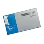
BLE113
DATA SHEET
Friday, 06 March 2015
Version 1.45
�Copyright © 2000-2015 Bluegiga Technologies
All rights reserved.
Bluegiga Technologies assumes no responsibility for any errors which may appear in this manual.
Furthermore, Bluegiga Technologies reserves the right to alter the hardware, software, and/or specifications
detailed here at any time without notice and does not make any commitment to update the information
contained here. Bluegiga’s products are not authorized for use as critical components in life support devices
or systems.
The WRAP is a registered trademark of Bluegiga Technologies
The Bluetooth trademark is owned by the Bluetooth SIG Inc., USA and is licensed to Bluegiga Technologies.
All other trademarks listed herein are owned by their respective owners.
Bluegiga Technologies Oy
�VERSION HISTORY
Version
Comment
1.0
Preliminary datasheet -> production datasheet. No changes
1.1
Pull-up resistors added to P1_0 and P1_1 in the example schematic
1.2
5 mm restriction removed from the FCC statement
1.3
Product code for 256k variant added. Peripheral mapping table: analog
comparator added. Added note that pins configured as peripheral I/O signals
do not have pull-up / -down capability. RF Characteristics added.
1.4
Product numbering updated
1.41
CE info
1.42
Updated FCC ID in one incorrect location
1.43
PIO current drive capability figures added
1.44
Current consumption profile added
1.45
SPI slave mode removed
Bluegiga Technologies Oy
�TABLE OF CONTENTS
1
BLE113 Product numbering ..........................................................................................................................6
2
Pinout and Terminal Description ...................................................................................................................7
2.1
I/O Ports .............................................................................................................................................. 10
2.2
UART ................................................................................................................................................... 10
2.3
Electrical Characteristics ..................................................................................................................... 11
2.4
Absolute Maximum Ratings ................................................................................................................ 11
2.5
Recommended Operating Conditions ................................................................................................. 11
2.6
DC Characteristics .............................................................................................................................. 11
2.7
Current Consumption .......................................................................................................................... 13
2.8
RF Characteristics ............................................................................................................................... 14
2.9
Antenna characteristics ....................................................................................................................... 15
3
Physical Dimensions .................................................................................................................................. 18
4
Power-On Reset and Brownout Detector ................................................................................................... 20
5
Design Guidelines ...................................................................................................................................... 21
5.1
General Design Guidelines ................................................................................................................. 21
5.2
Layout Guide Lines ............................................................................................................................. 21
5.3
BLE113-A Layout Guide ..................................................................................................................... 22
6
Soldering Recommendations ..................................................................................................................... 24
7
Block diagram ............................................................................................................................................. 25
8
Certifications ............................................................................................................................................... 28
8.1
Bluetooth ............................................................................................................................................. 28
8.2
FCC and IC ......................................................................................................................................... 28
8.2.1
9
FCC et IC ..................................................................................................................................... 29
8.3
CE ....................................................................................................................................................... 31
8.4
MIC Japan ........................................................................................................................................... 31
8.5
KCC (Korea) ........................................................................................................................................ 31
Contact Information .................................................................................................................................... 32
Bluegiga Technologies Oy
�BLE113 Bluetooth® Smart Module
DESCRIPTION
BLE113 is a Bluetooth Smart module targeted
for small and low power sensors and
accessories. It integrates all features required
for a Bluetooth Smart application: Bluetooth
radio, software stack and GATT based
profiles.
BLE113 Bluetooth Smart module can also host
end user applications, which means no
external micro controller is required in size or
price constrained devices.
BLE113 module has flexible hardware
interfaces to connect to different peripherals
and sensors. BLE113 can be powered directly
from a standard 3V coin cell battery or pair of
AAA batteries.
KEY FEATURES:
In lowest power sleep mode it consumes only
500nA and will wake up in few hundred
microseconds.
APPLICATIONS:
Health and fitness sensors
Medical sensors
iPhone and iPad accessories
Security and proximity tags
Key fobs
Smart home sensors and collectors
Wireless keys
HID keyboards and mice
Bluetooth v. 4.0, single mode compliant
o Supports master and slave modes
o Up to eight connections
Integrated Bluetooth Smart stack
o GAP, GATT, L2CAP and SMP
o Bluetooth Smart profiles
Radio performance
o TX power : 0 dBm to -23 dBm
o Receiver sensitivity: -93 dBm
Ultra low current consumption
o Transmit: 18.2 mA (0dBm)
o Transmit: 14.3 mA (0dBm +
DC/DC)
o Receive: 14.3 mA
o Sleep mode 3: 0.4 uA
Flexible peripheral interfaces
o UART and SPI
o I2C, PWM and GPIO
o 12-bit ADC
Host interfaces:
o UART
Programmable 8051 processor for standalone operation
Dimensions: 9.15 x 15.75 x 2.1 mm
Bluetooth, CE, FCC, IC, South Korea and
Japan qualified
Bluegiga Technologies Oy
�1 BLE113 Product numbering
Product code
Description
BLE113-A
BLE113 with integrated chip antenna, 128k flash memory
BLE113-A-M256K
BLE113 with integrated chip antenna, 256k flash memory
Bluegiga Technologies Oy
Page 6 of 32
�GND
2
3
4
5
6
7
8
9
10
11
12
13
14
15
16
17
18
GND
GND
GND
GND
GND
GND
AVDD
P2_2
P2_1
P2_0
P1_7
P1_6
SCL
SDA
NC
DVDD
GND
GND
NC
Reset#
P0_0
P0_1
P0_2
P0_3
P0_4
P0_5
P0_6
P0_7
GND
36
35
34
33
32
31
30
29
28
27
26
25
19
20
21
22
23
24
1
P1_5
P1_4
P1_3
P1_2
P1_1
P1_0
2 Pinout and Terminal Description
Figure 1: BLE113
RESET
34
Active low reset. Internal pull-up.
GND
1 - 7, 18,
25, 36
GND
DVDD
AVDD
17
8
Supply voltage
Supply voltage
GND
Supply voltage 2V - 3.6V
Supply voltage 2V - 3.6V
Table 1: Supply and RF Terminal Descriptions
Bluegiga Technologies Oy
Page 7 of 32
�PIN
PIN NAME PIN TYPE
NUMBER
DESCRIPTION
9
P2_2
10
P2_1
11
12
13
19
20
21
22
26
27
28
29
30
31
32
33
P2_0
P1_7
P1_6
P1_5
P1_4
P1_3
P1_2
P0_7
P0_6
P0_5
P0_4
P0_3
P0_2
P0_1
P0_0
23
P1_1
24
P1_0
14
SCL
I2C clock or digital I/O
Can be used as I2C clock pin or digital I/O. Leave
floating if not used. If grounded disable pull up.
15
SDA
I2C data or digital I/O
Can be used as I2C data pin or digital I/O. Leave
floating if not used. If grounded disable pull up.
Digital I/O
Configurable I/O port, See table 3
Digital I/O
Configurable I/O port with 20mA driving
capability, See table 3
Table 2: Terminal Descriptions
Bluegiga Technologies Oy
Page 8 of 32
�PERIPHERAL /
FUNCTION
Analog Comparator
ADC
USART 0 SPI (**
USART 0 UART
USART 1 SPI (**
USART 1 UART
TIMER 1
TIMER 3
TIMER 4
P0
5
4
3
2
1
0
+
A7 A6 A5 A4 A3 A2 A1 A0
7
6
C
Alt.1
P1
7
6
3
2
1
0
2
P2
1
HARDWARE.XML Example (*
0
SS MO MI
很抱歉,暂时无法提供与“BLE113-A-M256K”相匹配的价格&库存,您可以联系我们找货
免费人工找货