C8051F015
25 MIPS, 32 kB Flash, 10-Bit ADC, 64-Pin Mixed-Signal MCU
Analog Peripherals
10-Bit ADC
High-Speed 8051 µC Core
-
-
±1 LSB INL; no missing codes Programmable throughput up to 100 ksps 8 external inputs; programmable as single-ended or differential Programmable amplifier gain: 16, 8, 4, 2, 1, 0.5 Data-dependent windowed interrupt generator Built-in temperature sensor (±3 °C) Voltage output 10 µsec settling time 16 programmable hysteresis values Configurable to generate interrupts or reset
Pipelined instruction architecture; executes 70% of Instructions in 1 or 2 system clocks Up to 25 MIPS throughput with 25 MHz clock Expanded interrupt handler; up to 21 interrupt sources 2304 bytes data RAM 32 kB Flash; in-system programmable in 512-byte sectors (512 bytes are reserved) 32 port I/O; all are 5 V tolerant Hardware SMBus™ (I2C™ compatible), SPI™, and UART serial ports available concurrently Programmable 16-bit counter/timer array with five capture/compare modules 4 general-purpose 16-bit counter/timers Dedicated watchdog timer; bidirectional reset Internal programmable oscillator: 2–16 MHz External oscillator: Crystal, RC, C, or Clock Can switch between clock sources on-the-fly 64-pin TQFP (standard lead and lead-free packages) Lead-free package: C8051F015-GQ Standard package: C8051F015
Memory
Two 12-Bit DACs
Digital Peripherals
Two Comparators
Internal Voltage Reference VDD Monitor/Brown-out Detector
On-Chip JTAG Debug
-
On-chip emulation circuitry facilitates full-speed, non-intrusive, in-circuit emulation Supports breakpoints, single stepping, watchpoints, inspect/modify memory, and registers Superior performance to emulation systems using ICE-chips, target pods, and sockets Fully compliant with IEEE 1149.1 specification Typical operating current: 12.5 mA at 25 MHz Multiple power saving sleep and shutdown modes
Clock Sources
Package Ordering Part Numbers
Supply Voltage: 2.7 to 3.6 V Temperature Range: –40 to +85 °C
VDD VDD VDD DGND DGND DGND AV+ AV+ AGND AGND TCK TMS TDI TDO RST
Digital Power
UART SMBus SPI Bus
Analog Power
5-Chnl PCA Boundary Scan Debug HW
Reset
JTAG Logic
VDD Monitor
XTAL1 XTAL2
WDT
8 0 5 1 C o r e
32 kB FLASH 256 Byte RAM 2048 Byte XRAM
Timers 0,1,2 Timer 3 Port 0 Latch Port 1 Latch Port 2 Latch
C R O S S B A R S W I T C H
P 0 D r v P 1 D r v P 2 D r v P 3 D r v
P0.0 P0.1 P0.2 P0.3 P0.4 P0.5 P0.6 P0.7 P1.0 P1.1 P1.2 P1.3 P1.4 P1.5 P1.6 P1.7 P2.0 P2.1 P2.2 P2.3 P2.4 P2.5 P2.6 P2.7 P3.0 P3.1 P3.2 P3.3 P3.4 P3.5 P3.6 P3.7
External Oscillator Circuit Internal Oscillator
System Clock
SFR Bus
Port 3 Latch
VREF DAC1
VREF DAC1 (12-Bit) DAC0 (12-Bit)
DAC0 AIN0.0 AIN0.1 AIN0.2 AIN0.3 AIN0.4 AIN0.5 AIN0.6 AIN0.7 CP0+ CP0CP1+ CP1-
A M U X
Prog Gain
ADC 100 ksps (10-Bit)
TEMP SENSOR
CP0 CP1
Precision Mixed Signal
Copyright © 2005 by Silicon Laboratories
5.5.2005
�C8051F015
25 MIPS, 32 kB Flash, 10-Bit ADC, 64-Pin Mixed-Signal MCU Selected Electrical Specifications
(TA = –40 to +85 C°, VDD = 2.7 V unless otherwise specified)
PARAMETER CONDITIONS GLOBAL CHARACTERISTICS Analog Supply Voltage Analog Supply Current Internal REF, ADC, DAC, Comparators all active Analog Supply Current with Internal REF, ADC, DAC, Comparators all analog sub-systems inactive disabled Digital Supply Voltage Digital Supply Current with Clock = 25 MHz CPU active Clock = 1 MHz Clock = 32 kHz Digital Supply Current Oscillator not running (shutdown mode) VDD Data Retention Voltage RAM remains valid CPU & DIGITAL I/O Clock Frequency Range Port Output High Voltage IOH = –3 mA, Port I/O push-pull Port Output Low Voltage IOL = 8.5 mA Input High Voltage Input Low Voltage SMBus SCL Frequency SYSCLK = MCU system clock SPI Bus Clock Frequency SYSCLK = MCU system clock A/D CONVERTER Resolution Integral Nonlinearity Differential Nonlinearity Guaranteed Monotonic Throughput Rate Input Voltage Range D/A CONVERTERS Resolution Integral Nonlinearity Specified from Data Word 014h to FEBh Differential Nonlinearity Guaranteed Monotonic Offset Error Data Word = 014h Output Settling Time To ½ LSB of full-scale Output Voltage Swing COMPARATORS Supply Current (each Comparator) Response Time | (CP+) – (CP-) | = 100 mV Input Voltage Range Input Bias Current Input Offset Voltage MIN 2.7 0.8 5 2.7 12 0.5 20 2 1.5 DC VDD – 0.7 0.8 x VDD 0.2 x VDD SYSCLK/8 SYSCLK/2 10 ±1 ±1 100 VREF ±4 ±1 ±3 10 0 1.5 4 –0.25 –5 –10 0.001 (AV+) +0.25 +5 +10 VREF – 1 LSB 25 0.6 3.6 TYP MAX 3.6 UNITS V mA µA V mA mA µA µA V MHz V V V V MHz MHz bits LSB LSB ksps V bits LSB LSB LSB µs V µA µs V nA mV
0 12
Package Information
D D1
C8051F005DK Development Kit
MIN NOM MAX (mm) (mm) (mm) A 1.20 0.15 1.05
A1 0.05
E1 E
A2 0.95 b
0.17 0.22 0.27 12.00 10.00 0.50 12.00 10.00 -
64 PIN 1 DESIGNATOR 1 A2 e A b A1
D D1 e E E1
Precision Mixed Signal
Copyright © 2005 by Silicon Laboratories
5.5.2005
Silicon Laboratories and Silicon Labs are trademarks of Silicon Laboratories Inc. Other products or brandnames mentioned herein are trademarks or registered trademarks of their respective holders
�
很抱歉,暂时无法提供与“C8051F015”相匹配的价格&库存,您可以联系我们找货
免费人工找货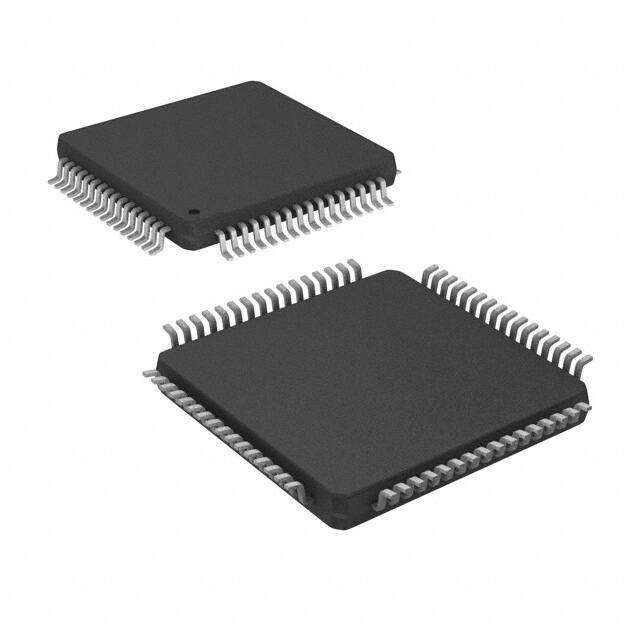


 工商网监
湘ICP备2023018690号
工商网监
湘ICP备2023018690号

