C8051F52x-53x
8/4/2 kB ISP Flash MCU Family
Analog Peripherals - 12-Bit ADC
• • • • • • • •
-
Comparator
±1 LSB INL (C8051F52x/C8051F53x); no missing codes Programmable throughput up to 200 ksps Up to 6/16 external inputs Data dependent windowed interrupt generator Built-in temperature sensor Programmable hysteresis and response time Configurable as wake-up or reset source Low current
Memory - 8/4/2 kB Flash; In-system byte programmable in
512 byte sectors
- 256 bytes internal data RAM Digital Peripherals - 16/6 port I/O; push-pull or open-drain, 5 V tolerant - Hardware SPI™, and UART serial port - Hardware LIN (both master and slave, compatible with V1.3 and V2.0) Three general purpose 16-bit counter/timers Programmable 16-bit counter/timer array with three capture/compare modules, WDT
- POR/Brownout Detector - Voltage Reference—1.5 to 2.2 V (programmable) On-Chip Debug - On-chip debug circuitry facilitates full-speed, nonSupply Voltage 2.7 to 5.25 V - Built-in LDO regulator High Speed 8051 µC Core - Pipelined instruction architecture; executes 70% of instructions in 1 or 2 system clocks Up to 25 MIPS throughput with 25 MHz system clock Expanded interrupt handler intrusive in-system debug (No emulator required) Provides breakpoints, single stepping Inspect/modify memory and registers Complete development kit
Clock Sources - Internal oscillators: 24.5 MHz ±0.5% accuracy supports UART and LIN-Master operation External oscillator: Crystal, RC, C, or Clock (1 or 2 pin modes) Can switch between clock sources on-the-fly
Packages: - 10-Pin QFN (3 x 3 mm) - 20-pin QFN (4 x 4 mm) - 20-pin TSSOP Temperature Range: –40 to +125 °C
A NALOG PERIPHERALS
A M U X
DIGITAL I/O
UART SPI PCA Timer 0 Timer 1 Timer 2 Port 0 CROSSBAR Port 1 LIN
12-bit 200 ksps ADC
+ VOLTAGE COMPARATOR
TEMP SENSOR
VREF
VREG
24.5 MHz High Precision (±0.5%) Internal Oscillator
HIGH-SPEED CONTROLLER CORE 8/4/2 kB ISP FLASH FLEXIBLE INTERRUPTS 8051 CPU (25 MIPS) D EBUG CIRCUITRY 256 B SRAM POR W DT
Rev. 0.3 5/07
Copyright © 2007 by Silicon Laboratories
C8051F52x-53x
�C8051F52x-53x
NOTES:
2
Rev. 0.3
�C8051F52x-53x
Table of Contents
1. System Overview.................................................................................................... 17 1.1. CIP-51™ Microcontroller................................................................................... 21 1.1.1. Fully 8051 Compatible Instruction Set...................................................... 21 1.1.2. Improved Throughput ............................................................................... 21 1.1.3. Additional Features .................................................................................. 21 1.1.4. On-Chip Debug Circuitry .......................................................................... 21 1.2. On-Chip Memory............................................................................................... 22 1.3. Operating Modes .............................................................................................. 24 1.4. 12-Bit Analog to Digital Converter..................................................................... 25 1.5. Programmable Comparator .............................................................................. 26 1.6. Voltage Regulator ............................................................................................. 26 1.7. Serial Port ......................................................................................................... 26 1.8. Port Input/Output............................................................................................... 27 2. Absolute Maximum Ratings .................................................................................. 29 3. Global DC Electrical Characteristics .................................................................... 30 4. Pinout and Package Definitions............................................................................ 31 5. 12-Bit ADC (ADC0).................................................................................................. 41 5.1. Analog Multiplexer ............................................................................................ 41 5.2. Temperature Sensor ......................................................................................... 42 5.3. ADC0 Operation................................................................................................ 42 5.3.1. Starting a Conversion............................................................................... 43 5.3.2. Tracking Modes........................................................................................ 43 5.3.3. Timing....................................................................................................... 44 5.3.4. Burst Mode ............................................................................................... 46 5.3.5. Output Conversion Code.......................................................................... 47 5.3.6. Settling Time Requirements ..................................................................... 48 5.4. Programmable Window Detector ...................................................................... 53 5.4.1. Window Detector In Single-Ended Mode ................................................. 56 5.5. Selectable Attenuation ...................................................................................... 57 5.6. Typical ADC Parameters and Description ........................................................ 57 5.6.1. Resolution ................................................................................................ 57 5.6.2. Integral Non-Linearity (INL) ...................................................................... 57 5.6.3. Differential Non-Linearity (DNL) ............................................................... 57 5.6.4. Offset ....................................................................................................... 58 5.6.5. Full-Scale ................................................................................................. 58 5.6.6. Signal to Noise Plus Distortion ................................................................. 58 5.6.7. Total Harmonic Distortion (THD) .............................................................. 59 5.6.8. Spurious Free Dynamic Range (SFDR) ................................................... 59 6. Voltage Reference .................................................................................................. 63 7. Voltage Regulator (REG0)...................................................................................... 67 8. Comparator ........................................................................................................... 69 9. CIP-51 Microcontroller ........................................................................................... 75 9.1. Instruction Set ................................................................................................... 76
Rev. 0.3
3
�C8051F52x-53x
9.1.1. Instruction and CPU Timing ..................................................................... 76 9.1.2. MOVX Instruction and Program Memory ................................................. 77 9.2. Register Descriptions........................................................................................ 80 9.3. Power Management Modes .............................................................................. 83 9.3.1. Idle Mode.................................................................................................. 84 9.3.2. Stop Mode ................................................................................................ 84 10. Memory Organization and SFRs ........................................................................... 85 10.1.Program Memory.............................................................................................. 85 10.2.Data Memory .................................................................................................... 86 10.3.General Purpose Registers .............................................................................. 86 10.4.Bit Addressable Locations ................................................................................ 86 10.5.Stack................................................................................................................. 86 10.6.Special Function Registers............................................................................... 87 11. Interrupt Handler .................................................................................................... 91 11.1.MCU Interrupt Sources and Vectors................................................................. 91 11.2.Interrupt Priorities ............................................................................................. 91 11.3.Interrupt Latency............................................................................................... 91 11.4.Interrupt Register Descriptions ......................................................................... 93 11.5.External Interrupts ............................................................................................ 97 12. Reset Sources......................................................................................................... 99 12.1.Power-On Reset ............................................................................................. 100 12.2.Power-Fail Reset / VDD Monitor .................................................................... 101 12.3.External Reset ................................................................................................ 102 12.4.Missing Clock Detector Reset ........................................................................ 102 12.5.Comparator Reset .......................................................................................... 102 12.6.PCA Watchdog Timer Reset .......................................................................... 103 12.7.Flash Error Reset ........................................................................................... 103 12.8.Software Reset ............................................................................................... 103 13. Flash Memory ....................................................................................................... 107 13.1.Programming The Flash Memory ................................................................... 107 13.1.1.Flash Lock and Key Functions ............................................................... 107 13.1.2.Flash Erase Procedure .......................................................................... 108 13.1.3.Flash Write Procedure ........................................................................... 108 13.2.Flash Write and Erase Guidelines .................................................................. 109 13.2.1.VDD Maintenance and the VDD monitor ................................................. 110 13.2.2.PSWE Maintenance ............................................................................... 111 13.2.3.System Clock ......................................................................................... 111 13.3.Non-volatile Data Storage .............................................................................. 112 13.4.Security Options ............................................................................................. 112 14. Port Input/Output.................................................................................................. 117 14.1.Priority Crossbar Decoder .............................................................................. 119 14.2.Port I/O Initialization ....................................................................................... 123 14.3.General Purpose Port I/O ............................................................................... 125 15. Oscillators ............................................................................................................. 133 15.1.Programmable Internal Oscillator ................................................................... 133
4 Rev. 0.3
�C8051F52x-53x
15.1.1.Internal Oscillator Suspend Mode .......................................................... 134 15.2.External Oscillator Drive Circuit...................................................................... 137 15.2.1.Clocking Timers Directly Through the External Oscillator...................... 137 15.2.2.External Crystal Example....................................................................... 137 15.2.3.External RC Example............................................................................. 139 15.2.4.External Capacitor Example................................................................... 139 15.3.System Clock Selection.................................................................................. 141 16. UART0.................................................................................................................... 143 16.1.Enhanced Baud Rate Generation................................................................... 144 16.2.Operational Modes ......................................................................................... 145 16.2.1.8-Bit UART ............................................................................................. 145 16.2.2.9-Bit UART ............................................................................................. 146 16.3.Multiprocessor Communications .................................................................... 146 17. LIN (C8051F520/523/526/530/533/536 only) ........................................................ 151 17.1.Major Characteristics...................................................................................... 151 17.2. Software Interface with the LIN Peripheral .................................................. 152 17.3.LIN Registers.................................................................................................. 153 17.3.1.LIN Direct Access SFR Registers Definition .......................................... 153 17.3.2.LIN Indirect Access SFR Registers Definition........................................ 154 17.4.LIN Interface Setup and Operation................................................................. 161 17.4.1.Mode Definition ...................................................................................... 161 17.4.2.Bit Rate Options: Manual or Autobaud (Slave only)............................... 162 17.4.3.Baud Rate Calculations - Manual Mode................................................. 162 17.4.4.Baud Rate Calculations - Automatic Mode ............................................ 164 17.4.5.LIN Master Mode Operation................................................................... 165 17.4.6.LIN Slave Mode Operation..................................................................... 166 17.4.7.Sleep Mode and Wake-Up ..................................................................... 167 17.4.8.Error Detection and Handling................................................................. 168 17.4.9.LIN Master Mode Operation................................................................... 168 17.4.10.LIN Slave Mode Operation................................................................... 168 18. Enhanced Serial Peripheral Interface (SPI0)...................................................... 171 18.1.Signal Descriptions......................................................................................... 172 18.1.1.Master Out, Slave In (MOSI).................................................................. 172 18.1.2.Master In, Slave Out (MISO).................................................................. 172 18.1.3.Serial Clock (SCK) ................................................................................. 172 18.1.4.Slave Select (NSS) ................................................................................ 172 18.2.SPI0 Master Mode Operation ......................................................................... 173 18.3.SPI0 Slave Mode Operation ........................................................................... 174 18.4.SPI0 Interrupt Sources ................................................................................... 175 18.5.Serial Clock Timing......................................................................................... 175 18.6.SPI Special Function Registers ...................................................................... 176 19. Timers.................................................................................................................... 185 19.1.Timer 0 and Timer 1 ....................................................................................... 185
Rev. 0.3
5
�C8051F52x-53x
19.1.1.Mode 0: 13-bit Counter/Timer ................................................................ 185 19.1.2.Mode 1: 16-bit Counter/Timer ................................................................ 187 19.1.3.Mode 2: 8-bit Counter/Timer with Auto-Reload...................................... 187 19.1.4.Mode 3: Two 8-bit Counter/Timers (Timer 0 Only)................................. 188 19.2.Timer 2 .......................................................................................................... 193 19.2.1.16-bit Timer with Auto-Reload................................................................ 193 19.2.2.8-bit Timers with Auto-Reload................................................................ 194 19.2.3.External Capture Mode .......................................................................... 195 20. Programmable Counter Array (PCA0) ................................................................ 199 20.1.PCA Counter/Timer ........................................................................................ 200 20.2.Capture/Compare Modules ............................................................................ 201 20.2.1.Edge-triggered Capture Mode................................................................ 202 20.2.2.Software Timer (Compare) Mode........................................................... 203 20.2.3.High Speed Output Mode....................................................................... 204 20.2.4.Frequency Output Mode ........................................................................ 205 20.2.5.8-Bit Pulse Width Modulator Mode......................................................... 206 20.2.6.16-Bit Pulse Width Modulator Mode....................................................... 207 20.3.Watchdog Timer Mode ................................................................................... 207 20.3.1.Watchdog Timer Operation .................................................................... 208 20.3.2.Watchdog Timer Usage ......................................................................... 209 20.4.Register Descriptions for PCA........................................................................ 211 21. Revision Specific Behavior ................................................................................. 215 21.1.Revision Identification..................................................................................... 215 21.2.Reset Behavior ............................................................................................... 216 21.3.UART Pins...................................................................................................... 216 21.4.LIN .................................................................................................................. 216 21.4.1.Stop Bit Check ....................................................................................... 216 21.4.2.Synch Break and Synch Field Length Check......................................... 216 22. C2 Interface ........................................................................................................... 217 22.1.C2 Interface Registers.................................................................................... 217 22.2.C2 Pin Sharing ............................................................................................... 219 Contact Information.................................................................................................. 220
6
Rev. 0.3
�C8051F52x-53x
List of Figures
1. System Overview Figure 1.1. C8051F530 Block Diagram .................................................................... 19 Figure 1.2. C8051F520 Block Diagram .................................................................... 20 Figure 1.3. Development/In-System Debug Diagram............................................... 22 Figure 1.4. Memory Map .......................................................................................... 23 Figure 1.5. 12-Bit ADC Block Diagram..................................................................... 25 Figure 1.6. Comparator Block Diagram.................................................................... 26 Figure 1.7. Port I/O Functional Block Diagram......................................................... 27 2. Absolute Maximum Ratings 3. Global DC Electrical Characteristics 4. Pinout and Package Definitions Figure 4.1. TSSOP-20 Package Diagram ................................................................ 37 Figure 4.2. QFN-20 Package Diagram..................................................................... 38 Figure 4.3. QFN-10 Package Diagram..................................................................... 39 5. 12-Bit ADC (ADC0) Figure 5.1. ADC0 Functional Block Diagram............................................................ 41 Figure 5.2. Typical Temperature Sensor Transfer Function..................................... 42 Figure 5.3. ADC0 Tracking Modes ........................................................................... 44 Figure 5.4. 12-Bit ADC Tracking Mode Example ..................................................... 45 Figure 5.5. 12-Bit ADC Burst Mode Example with Repeat Count Set to 4............... 46 Figure 5.6. ADC0 Equivalent Input Circuits.............................................................. 48 Figure 5.7. ADC Window Compare Example: Right-Justified Single-Ended Data ... 56 Figure 5.8. ADC Window Compare Example: Left-Justified Single-Ended Data ..... 56 6. Voltage Reference Figure 6.1. Voltage Reference Functional Block Diagram ....................................... 63 7. Voltage Regulator (REG0) Figure 7.1. External Capacitors for Voltage Regulator Input/Output ........................ 67 8. Comparator Figure 8.1. Comparator Functional Block Diagram .................................................. 69 Figure 8.2. Comparator Hysteresis Plot ................................................................... 70 9. CIP-51 Microcontroller Figure 9.1. CIP-51 Block Diagram............................................................................ 75 10. Memory Organization and SFRs Figure 10.1. Memory Map ........................................................................................ 85 11. Interrupt Handler 12. Reset Sources Figure 12.1. Reset Sources...................................................................................... 99 Figure 12.2. Power-On and VDD Monitor Reset Timing ......................................... 100 13. Flash Memory Figure 13.1. Flash Program Memory Map.............................................................. 112 14. Port Input/Output Figure 14.1. Port I/O Functional Block Diagram ..................................................... 117 Figure 14.2. Port I/O Cell Block Diagram ............................................................... 118
Rev. 0.3
7
�C8051F52x-53x
Figure 14.3. Crossbar Priority Decoder with No Pins Skipped (TSSOP 20 and QFN 20) .................................................................................. 119 Figure 14.4. Crossbar Priority Decoder with Crystal Pins Skipped (TSSOP 20 and QFN 20) .................................................................................. 120 Figure 14.5. Crossbar Priority Decoder with No Pins Skipped (QFN 10) ............... 121 Figure 14.6. Crossbar Priority Decoder with Crystal Pins Skipped (QFN 10) ........ 122 15. Oscillators Figure 15.1. Oscillator Diagram.............................................................................. 133 Figure 15.2. 32 kHz External Crystal Example....................................................... 138 16. UART0 Figure 16.1. UART0 Block Diagram ....................................................................... 143 Figure 16.2. UART0 Baud Rate Logic .................................................................... 144 Figure 16.3. UART Interconnect Diagram .............................................................. 145 Figure 16.4. 8-Bit UART Timing Diagram............................................................... 145 Figure 16.5. 9-Bit UART Timing Diagram............................................................... 146 Figure 16.6. UART Multi-Processor Mode Interconnect Diagram .......................... 147 17. LIN (C8051F520/523/526/530/533/536 only) Figure 17.1. LIN Flowchart ..................................................................................... 151 18. Enhanced Serial Peripheral Interface (SPI0) Figure 18.1. SPI Block Diagram ............................................................................. 171 Figure 18.2. Multiple-Master Mode Connection Diagram ....................................... 174 Figure 18.3. 3-Wire Single Master and Slave Mode Connection Diagram ............. 174 Figure 18.4. 4-Wire Single Master and Slave Mode Connection Diagram ............. 174 Figure 18.5. Data/Clock Timing Relationship ......................................................... 176 Figure 18.6. SPI Master Timing (CKPHA = 0)........................................................ 181 Figure 18.7. SPI Master Timing (CKPHA = 1)........................................................ 181 Figure 18.8. SPI Slave Timing (CKPHA = 0).......................................................... 182 Figure 18.9. SPI Slave Timing (CKPHA = 1).......................................................... 182 19. Timers Figure 19.1. T0 Mode 0 Block Diagram.................................................................. 186 Figure 19.2. T0 Mode 2 Block Diagram.................................................................. 187 Figure 19.3. T0 Mode 3 Block Diagram.................................................................. 188 Figure 19.4. Timer 2 16-Bit Mode Block Diagram .................................................. 193 Figure 19.5. Timer 2 8-Bit Mode Block Diagram .................................................... 194 Figure 19.6. Timer 2 Capture Mode Block Diagram ............................................... 195 20. Programmable Counter Array (PCA0) Figure 20.1. PCA Block Diagram............................................................................ 199 Figure 20.2. PCA Counter/Timer Block Diagram.................................................... 200 Figure 20.3. PCA Interrupt Block Diagram ............................................................. 201 Figure 20.4. PCA Capture Mode Diagram.............................................................. 202 Figure 20.5. PCA Software Timer Mode Diagram .................................................. 203 Figure 20.6. PCA High-Speed Output Mode Diagram............................................ 204 Figure 20.7. PCA Frequency Output Mode ............................................................ 205 Figure 20.8. PCA 8-Bit PWM Mode Diagram ......................................................... 206 Figure 20.9. PCA 16-Bit PWM Mode...................................................................... 207
8 Rev. 0.3
�C8051F52x-53x
Figure 20.10. PCA Module 2 with Watchdog Timer Enabled ................................. 208 21. Revision Specific Behavior Figure 21.1. Device Package - TSSOP 20 ............................................................. 215 Figure 21.2. Device Package - QFN 20.................................................................. 215 Figure 21.3. Device Package - QFN 10.................................................................. 216 22. C2 Interface Figure 22.1. Typical C2 Pin Sharing....................................................................... 219
Rev. 0.3
9
�C8051F52x-53x
NOTES:
10
Rev. 0.3
�C8051F52x-53x
List of Tables
1. System Overview Table 1.1. Product Selection Guide ......................................................................... 18 Table 1.2. Operating Modes Summary .................................................................... 24 2. Absolute Maximum Ratings Table 2.1.Absolute Maximum Ratings..................................................................... 29 3. Global DC Electrical Characteristics Table 3.1.Global DC Electrical Characteristics........................................................ 30 4. Pinout and Package Definitions Table 4.1. Pin Definitions for the C8051F520 (QFN 10) .......................................... 31 Table 4.2. Pin Definitions for the C8051F530 (TSSOP 20) ..................................... 33 Table 4.3. Pin Definitions for the C8051F530 (QFN 20) .......................................... 35 Table 4.4. TSSOP-20 Package Diagram Dimensions ............................................. 37 Table 4.5. QFN-20 Package Diagram Dimensions ................................................. 38 Table 4.6. QFN-10 Package Diagram Dimensions ................................................. 39 5. 12-Bit ADC (ADC0) Table 5.1.ADC0 Electrical Characteristics (VDD = 2.6 V, VREF = 1.5 V) ................. 60 Table 5.2.ADC0 Electrical Characteristics (VDD = 2.1 V, VREF = 1.5 V) ................. 61 6. Voltage Reference Table 6.1.Voltage Reference Electrical Characteristics .......................................... 65 7. Voltage Regulator (REG0) Table 7.1.Voltage Regulator Electrical Specifications ............................................. 68 8. Comparator Table 8.1.Comparator Electrical Characteristics ..................................................... 74 9. CIP-51 Microcontroller Table 9.1. CIP-51 Instruction Set Summary ............................................................ 77 10. Memory Organization and SFRs Table 10.1. Special Function Register (SFR) Memory Map .................................... 87 Table 10.2. Special Function Registers ................................................................... 88 11. Interrupt Handler Table 11.1. Interrupt Summary ................................................................................ 92 12. Reset Sources Table 12.1.Reset Electrical Characteristics........................................................... 105 13. Flash Memory Table 13.1. Flash Security Summary .................................................................... 114 Table 13.2.Flash Electrical Characteristics ........................................................... 116 14. Port Input/Output Table 14.1.Port I/O DC Electrical Characteristics.................................................. 132 15. Oscillators Table 15.1.Oscillator Electrical Characteristics ..................................................... 142 Table 15.2.Oscillator Wake-Up Time from Suspend Mode ................................... 142 16. UART0 Table 16.1. Timer Settings for Standard Baud Rates Using the Internal Oscillator ............................................................... 150
Rev. 0.3
11
�C8051F52x-53x
17. LIN (C8051F520/523/526/530/533/536 only) Table 17.1. LIN Registers (Indirectly Addressable) ............................................... 154 Table 17.2. Table Needs Title ............................................................................... 162 Table 17.3. Manual Bit-Rate Parameters Examples ............................................. 164 Table 17.4. Autobaud Parameters Examples ........................................................ 165 18. Enhanced Serial Peripheral Interface (SPI0) Table 18.1. SPI Slave Timing Parameters ............................................................ 183 19. Timers 20. Programmable Counter Array (PCA0) Table 20.1. PCA Timebase Input Options ............................................................. 200 Table 20.2. PCA0CPM Register Settings for PCA Capture/Compare Modules .... 201 Table 20.3. Watchdog Timer Timeout Intervals ..................................................... 210 21. Revision Specific Behavior 22. C2 Interface
12
Rev. 0.3
�C8051F52x-53x
List of Registers
SFR Definition 5.1. ADC0MX: ADC0 Channel Select . . . . . . . . . . . . . . . . . . . . . . . . . . 49 SFR Definition 5.2. ADC0CF: ADC0 Configuration . . . . . . . . . . . . . . . . . . . . . . . . . . . 50 SFR Definition 5.3. ADC0H: ADC0 Data Word MSB . . . . . . . . . . . . . . . . . . . . . . . . . . 51 SFR Definition 5.4. ADC0L: ADC0 Data Word LSB . . . . . . . . . . . . . . . . . . . . . . . . . . . 51 SFR Definition 5.5. ADC0CN: ADC0 Control . . . . . . . . . . . . . . . . . . . . . . . . . . . . . . . . 52 SFR Definition 5.6. ADC0TK: ADC0 Tracking Mode Select . . . . . . . . . . . . . . . . . . . . 53 SFR Definition 5.7. ADC0GTH: ADC0 Greater-Than Data High Byte . . . . . . . . . . . . . 54 SFR Definition 5.8. ADC0GTL: ADC0 Greater-Than Data Low Byte . . . . . . . . . . . . . . 54 SFR Definition 5.9. ADC0LTH: ADC0 Less-Than Data High Byte . . . . . . . . . . . . . . . . 55 SFR Definition 5.10. ADC0LTL: ADC0 Less-Than Data Low Byte . . . . . . . . . . . . . . . . 55 SFR Definition 6.1. REF0CN: Reference Control . . . . . . . . . . . . . . . . . . . . . . . . . . . . . 64 SFR Definition 7.1. REG0CN: Regulator Control . . . . . . . . . . . . . . . . . . . . . . . . . . . . . 68 SFR Definition 8.1. CPT0CN: Comparator0 Control . . . . . . . . . . . . . . . . . . . . . . . . . . . 71 SFR Definition 8.2. CPT0MX: Comparator0 MUX Selection . . . . . . . . . . . . . . . . . . . . 72 SFR Definition 8.3. CPT0MD: Comparator0 Mode Selection . . . . . . . . . . . . . . . . . . . . 73 SFR Definition 9.1. SP: Stack Pointer . . . . . . . . . . . . . . . . . . . . . . . . . . . . . . . . . . . . . . 80 SFR Definition 9.2. DPL: Data Pointer Low Byte . . . . . . . . . . . . . . . . . . . . . . . . . . . . . 81 SFR Definition 9.3. DPH: Data Pointer High Byte . . . . . . . . . . . . . . . . . . . . . . . . . . . . . 81 SFR Definition 9.4. PSW: Program Status Word . . . . . . . . . . . . . . . . . . . . . . . . . . . . . 82 SFR Definition 9.5. ACC: Accumulator . . . . . . . . . . . . . . . . . . . . . . . . . . . . . . . . . . . . . 83 SFR Definition 9.6. B: B Register . . . . . . . . . . . . . . . . . . . . . . . . . . . . . . . . . . . . . . . . . 83 SFR Definition 9.7. PCON: Power Control . . . . . . . . . . . . . . . . . . . . . . . . . . . . . . . . . . 84 SFR Definition 11.1. IE: Interrupt Enable . . . . . . . . . . . . . . . . . . . . . . . . . . . . . . . . . . . 93 SFR Definition 11.2. IP: Interrupt Priority . . . . . . . . . . . . . . . . . . . . . . . . . . . . . . . . . . . 94 SFR Definition 11.3. EIE1: Extended Interrupt Enable 1 . . . . . . . . . . . . . . . . . . . . . . . 95 SFR Definition 11.4. EIP1: Extended Interrupt Priority 1 . . . . . . . . . . . . . . . . . . . . . . . 96 SFR Definition 11.5. IT01CF: INT0/INT1 Configuration . . . . . . . . . . . . . . . . . . . . . . . . 98 SFR Definition 12.1. VDDMON: VDD Monitor Control . . . . . . . . . . . . . . . . . . . . . . . . 102 SFR Definition 12.2. RSTSRC: Reset Source . . . . . . . . . . . . . . . . . . . . . . . . . . . . . . 104 SFR Definition 13.1. PSCTL: Program Store R/W Control . . . . . . . . . . . . . . . . . . . . . 115 SFR Definition 13.2. FLKEY: Flash Lock and Key . . . . . . . . . . . . . . . . . . . . . . . . . . . 115 SFR Definition 14.1. XBR0: Port I/O Crossbar Register 0 . . . . . . . . . . . . . . . . . . . . . 124 SFR Definition 14.2. XBR1: Port I/O Crossbar Register 1 . . . . . . . . . . . . . . . . . . . . . 125 SFR Definition 14.3. P0: Port0 . . . . . . . . . . . . . . . . . . . . . . . . . . . . . . . . . . . . . . . . . . 126 SFR Definition 14.4. P0MDIN: Port0 Input Mode . . . . . . . . . . . . . . . . . . . . . . . . . . . . 126 SFR Definition 14.5. P0MDOUT: Port0 Output Mode . . . . . . . . . . . . . . . . . . . . . . . . . 127 SFR Definition 14.6. P0SKIP: Port0 Skip . . . . . . . . . . . . . . . . . . . . . . . . . . . . . . . . . . 127 SFR Definition 14.7. P0MAT: Port0 Match . . . . . . . . . . . . . . . . . . . . . . . . . . . . . . . . . 128 SFR Definition 14.8. P0MASK: Port0 Mask . . . . . . . . . . . . . . . . . . . . . . . . . . . . . . . . 128 SFR Definition 14.9. P1: Port1 . . . . . . . . . . . . . . . . . . . . . . . . . . . . . . . . . . . . . . . . . . 129 SFR Definition 14.10. P1MDIN: Port1 Input Mode . . . . . . . . . . . . . . . . . . . . . . . . . . . 129 SFR Definition 14.11. P1MDOUT: Port1 Output Mode . . . . . . . . . . . . . . . . . . . . . . . . 130 SFR Definition 14.12. P1SKIP: Port1 Skip . . . . . . . . . . . . . . . . . . . . . . . . . . . . . . . . . 130
Rev. 0.3
13
�C8051F52x-53x
SFR Definition 14.13. P0SKIP: Port0 Skip . . . . . . . . . . . . . . . . . . . . . . . . . . . . . . . . . 131 SFR Definition 14.14. P1MAT: Port1 Match . . . . . . . . . . . . . . . . . . . . . . . . . . . . . . . . 131 SFR Definition 14.15. P1MASK: Port1 Mask . . . . . . . . . . . . . . . . . . . . . . . . . . . . . . . 131 SFR Definition 15.1. OSCICN: Internal Oscillator Control . . . . . . . . . . . . . . . . . . . . . 135 SFR Definition 15.2. OSCICL: Internal Oscillator Calibration . . . . . . . . . . . . . . . . . . . 136 SFR Definition 15.3. OSCIFIN: Internal Fine Oscillator Calibration . . . . . . . . . . . . . . 136 SFR Definition 15.4. OSCXCN: External Oscillator Control . . . . . . . . . . . . . . . . . . . . 140 SFR Definition 15.5. CLKSEL: Clock Select . . . . . . . . . . . . . . . . . . . . . . . . . . . . . . . . 141 SFR Definition 16.1. SCON0: Serial Port 0 Control . . . . . . . . . . . . . . . . . . . . . . . . . . 148 SFR Definition 16.2. SBUF0: Serial (UART0) Port Data Buffer . . . . . . . . . . . . . . . . . 149 SFR Definition 17.1. LINADDR: Indirect Address Register . . . . . . . . . . . . . . . . . . . . . 153 SFR Definition 17.2. LINDATA: LIN Data Register . . . . . . . . . . . . . . . . . . . . . . . . . . . 153 SFR Definition 17.3. LINCF Control Mode Register . . . . . . . . . . . . . . . . . . . . . . . . . . 153 SFR Definition 17.4. LINDT1: LIN Data Byte . . . . . . . . . . . . . . . . . . . . . . . . . . . . . . . 154 SFR Definition 17.5. LINDT2: LIN Data Byte . . . . . . . . . . . . . . . . . . . . . . . . . . . . . . . 155 SFR Definition 17.6. LINDT3: LIN Data Byte . . . . . . . . . . . . . . . . . . . . . . . . . . . . . . . 155 SFR Definition 17.7. LINDT4: LIN Data Byte . . . . . . . . . . . . . . . . . . . . . . . . . . . . . . . 155 SFR Definition 17.8. LINDT5: LIN Data Byte . . . . . . . . . . . . . . . . . . . . . . . . . . . . . . . 155 SFR Definition 17.9. LINDT6: LIN Data Byte . . . . . . . . . . . . . . . . . . . . . . . . . . . . . . . 156 SFR Definition 17.10. LINDT7: LIN Data Byte . . . . . . . . . . . . . . . . . . . . . . . . . . . . . . 156 SFR Definition 17.11. LINDT8: LIN Data Byte . . . . . . . . . . . . . . . . . . . . . . . . . . . . . . 156 SFR Definition 17.12. LINCTRL: LIN Control Register . . . . . . . . . . . . . . . . . . . . . . . . 157 SFR Definition 17.13. LINST: LIN STATUS Register . . . . . . . . . . . . . . . . . . . . . . . . . 158 SFR Definition 17.14. LINERR: LIN ERROR Register . . . . . . . . . . . . . . . . . . . . . . . . 159 SFR Definition 17.15. LINSIZE: LIN Message Size Register . . . . . . . . . . . . . . . . . . . 160 SFR Definition 17.16. LINDIV: LIN Divider Register . . . . . . . . . . . . . . . . . . . . . . . . . . 160 SFR Definition 17.17. LINMUL: LIN Multiplier Register . . . . . . . . . . . . . . . . . . . . . . . 161 SFR Definition 17.18. LINID: LIN ID Register . . . . . . . . . . . . . . . . . . . . . . . . . . . . . . . 161 SFR Definition 18.1. SPI0CFG: SPI0 Configuration . . . . . . . . . . . . . . . . . . . . . . . . . . 177 SFR Definition 18.2. SPI0CN: SPI0 Control . . . . . . . . . . . . . . . . . . . . . . . . . . . . . . . . 178 SFR Definition 18.3. SPI0CKR: SPI0 Clock Rate . . . . . . . . . . . . . . . . . . . . . . . . . . . . 179 SFR Definition 18.4. SPI0DAT: SPI0 Data . . . . . . . . . . . . . . . . . . . . . . . . . . . . . . . . . 180 SFR Definition 19.1. TCON: Timer Control . . . . . . . . . . . . . . . . . . . . . . . . . . . . . . . . . 189 SFR Definition 19.2. TMOD: Timer Mode . . . . . . . . . . . . . . . . . . . . . . . . . . . . . . . . . . 190 SFR Definition 19.3. CKCON: Clock Control . . . . . . . . . . . . . . . . . . . . . . . . . . . . . . . 191 SFR Definition 19.4. TL0: Timer 0 Low Byte . . . . . . . . . . . . . . . . . . . . . . . . . . . . . . . . 192 SFR Definition 19.5. TL1: Timer 1 Low Byte . . . . . . . . . . . . . . . . . . . . . . . . . . . . . . . . 192 SFR Definition 19.6. TH0: Timer 0 High Byte . . . . . . . . . . . . . . . . . . . . . . . . . . . . . . . 192 SFR Definition 19.7. TH1: Timer 1 High Byte . . . . . . . . . . . . . . . . . . . . . . . . . . . . . . . 192 SFR Definition 19.8. TMR2CN: Timer 2 Control . . . . . . . . . . . . . . . . . . . . . . . . . . . . . 196 SFR Definition 19.9. TMR2RLL: Timer 2 Reload Register Low Byte . . . . . . . . . . . . . 197 SFR Definition 19.10. TMR2RLH: Timer 2 Reload Register High Byte . . . . . . . . . . . 197 SFR Definition 19.11. TMR2L: Timer 2 Low Byte . . . . . . . . . . . . . . . . . . . . . . . . . . . . 197 SFR Definition 19.12. TMR2H Timer 2 High Byte . . . . . . . . . . . . . . . . . . . . . . . . . . . . 197 SFR Definition 20.1. PCA0CN: PCA Control . . . . . . . . . . . . . . . . . . . . . . . . . . . . . . . 211
14 Rev. 0.3
�C8051F52x-53x
SFR Definition 20.2. PCA0MD: PCA Mode . . . . . . . . . . . . . . . . . . . . . . . . . . . . . . . . 212 SFR Definition 20.3. PCA0CPMn: PCA Capture/Compare Mode . . . . . . . . . . . . . . . 213 SFR Definition 20.4. PCA0L: PCA Counter/Timer Low Byte . . . . . . . . . . . . . . . . . . . 214 SFR Definition 20.5. PCA0H: PCA Counter/Timer High Byte . . . . . . . . . . . . . . . . . . . 214 SFR Definition 20.6. PCA0CPLn: PCA Capture Module Low Byte . . . . . . . . . . . . . . . 214 SFR Definition 20.7. PCA0CPHn: PCA Capture Module High Byte . . . . . . . . . . . . . . 214 C2 Register Definition 22.1. C2ADD: C2 Address . . . . . . . . . . . . . . . . . . . . . . . . . . . 217 C2 Register Definition 22.2. DEVICEID: C2 Device ID . . . . . . . . . . . . . . . . . . . . . . . . 217 C2 Register Definition 22.3. REVID: C2 Revision ID . . . . . . . . . . . . . . . . . . . . . . . . . 218 C2 Register Definition 22.4. FPCTL: C2 Flash Programming Control . . . . . . . . . . . . 218 C2 Register Definition 22.5. FPDAT: C2 Flash Programming Data . . . . . . . . . . . . . . 218
Rev. 0.3
15
�C8051F52x-53x
NOTES:
16
Rev. 0.3
�C8051F52x-53x
1. System Overview
The C8051F52x/C8051F53x family of devices are fully integrated, very low power, mixed-signal systemon-a-chip MCUs. Highlighted features are listed below. Refer to Table 1.1 for specific product feature selection. • • • • • • • • • • • • • High-speed pipelined 8051-compatible microcontroller core (up to 25 MIPS) In-system, full-speed, non-intrusive debug interface (on-chip) True 12-bit 200 ksps ADC with analog multiplexer and up to 16 analog inputs Precision programmable 24.5 MHz internal oscillator that is ±0.5% across voltage and temperature Up to 7680 bytes of on-chip Flash memory 256 bytes of on-chip RAM Enhanced UART, and SPI serial interfaces implemented in hardware LIN 2.0 peripheral (V2.0 and V1.3 compatible, master and slave modes) Three general-purpose 16-bit timers Programmable Counter/Timer Array (PCA) with three capture/compare modules and Watchdog Timer function On-chip Power-On Reset, VDD Monitor, and Temperature Sensor On-chip Voltage Comparator Up to 16 Port I/O
With on-chip Power-On Reset, VDD monitor, Watchdog Timer, and clock oscillator, the C8051F52x/F53x devices are truly standalone system-on-a-chip solutions. The Flash memory is byte writable and can be reprogrammed in-circuit, providing non-volatile data storage, and also allowing field upgrades of the 8051 firmware. User software has complete control of all peripherals, and may individually shut down any or all peripherals for power savings. The on-chip Silicon Laboratories 2-Wire (C2) Development Interface allows non-intrusive (uses no on-chip resources), full speed, in-circuit debugging using the production MCU installed in the final application. This debug logic supports inspection and modification of memory and registers, setting breakpoints, single stepping, run and halt commands. All analog and digital peripherals are fully functional while debugging using C2. The two C2 interface pins can be shared with user functions, allowing in-system programming and debugging without occupying package pins. Each device is specified for 2.7 to 5.25 V operation (supply voltage can be up to 5.25 V using on-chip regulator) over the automotive temperature range (–40 to +125 °C). The F52x is available in the QFN10 (3 x 3 mm) package. The F53x is available in the QFN20 (4 x 4 mm) or the TSSOP20 package.
Rev. 0.3
17
�C8051F52x-53x
Table 1.1. Product Selection Guide
Calibrated Internal 24.5 MHz Oscillator Tolerance
Programmable 3 Channels Counter Array
Internal Voltage Reference
12-bit ADC ±1 LSB INL
Ordering Part Number
Temperature Sensor
Analog Comparator
Timers (16-bit)
Flash Memory
MIPS (Peak)
Port I/Os
C8051F520-IM C8051F521-IM C8051F523-IM C8051F524-IM C8051F526-IM C8051F527-IM C8051F530-IM C8051F531-IM C8051F533-IM C8051F534-IM C8051F536-IM C8051F537-IM C8051F530-IT C8051F531-IT C8051F533-IT C8051F534-IT C8051F536-IT C8051F537-IT
25 8 kB 25 8 kB 25 4 kB 25 4 kB 25 2 kB 25 2 kB 25 8 kB 25 8 kB 25 4 kB 25 4 kB 25 2 kB 25 2 kB 25 8 kB 25 8 kB 25 4 kB 25 4 kB 25 2 kB 25 2 kB
256 256 256 256 256 256 256 256 256 256 256 256 256 256 256 256 256 256
0.5% 0.5% 0.5% 0.5% 0.5% 0.5% 0.5% 0.5% 0.5% 0.5% 0.5% 0.5% 0.5% 0.5% 0.5% 0.5% 0.5% 0.5%
3 3 3 3 3 3 3 3 3 3 3 3 3 3 3 3 3 3
6 6 6 6 6 6 16 16 16 16 16 16 16 16 16 16 16 16 — — — — — — — — —
QFN-10 QFN-10 QFN-10 QFN-10 QFN-10 QFN-10 QFN-20 QFN-20 QFN-20 QFN-20 QFN-20 QFN-20 TSSOP-20 TSSOP-20 TSSOP-20 TSSOP-20 TSSOP-20 TSSOP-20
18
Rev. 0.3
Package
UART
RAM
SPI
LIN
�C8051F52x-53x
(GPIO)
VREGIN
(2.7–5.25 V)
LDO
(VDD)
VDD GND
C2D
Debug HW
Reset
8 0 5 1 C o r e
UART0 S PI Bus
P 0
C R O S S B A R
P0.0/VREF P0.1 P0.2 P0.3 P0.4/TX P0.5/RX P0.6/C2D P0.7/XTAL1
SFR Bus
PCA(3 ch.) Timers 0,1,2
Port 0,1 Latch
D r v P 1 D r v
RST/C2CK
8 kB
Flash
LIN 2.0
P1.0/XTAL2 P1.1 P1.2/CNVSTR P1.3 P1.4 P1.5 P1.6 P1.7
VDD Monitor
XTAL1 XTAL2
WDT
VDD
External Oscillator Circuit
System Clock
256 bytes RAM
VREF
Reference Voltage
VREF
TEMP SENSOR
Precision Oscillator ±0.5%
A M U X
5 V ADC 200 ksps (12-Bit)
CP0
+ -
Figure 1.1. C8051F530 Block Diagram
Rev. 0.3
19
�C8051F52x-53x
(GPIO)
VREGIN
(2.7–5.25 V)
LDO
(VDD)
VDD GND
C2D
Debug HW
Reset
8 0 5 1 C o r e
UART0 SPI Bus
P0.0/VREF
SFR Bus
PCA(3 ch.) Timers 0,1,2
Port 0 Latch
RST/C2CK
8 kB
Flash
LIN 2.0
C R O S S B A R
P 0 D r v
P0.1/C2D P0.2/XTAL1 P0.3/XTAL2 P0.4/TX P0.5/RX/ CNVSTR
VDD Monitor
XTAL1 XTAL2
WDT
VDD
External Oscillator Circuit
System Clock
256 bytes RAM
VREF
Reference Voltage
VREF
TEMP SENSOR
Precision Oscillator ±0.5%
A M U X
5 V ADC 200 ksps (12-Bit)
CP0
+ -
Figure 1.2. C8051F520 Block Diagram
20
Rev. 0.3
�C8051F52x-53x
1.1. CIP-51™ Microcontroller
1.1.1. Fully 8051 Compatible Instruction Set
The C8051F52x/F53xdevices use Silicon Laboratories’ proprietary CIP-51 microcontroller core. The CIP51 is fully compatible with the MCS-51™ instruction set. Standard 803x/805x assemblers and compilers can be used to develop software. The C8051F52x/F53xfamily has a superset of all the peripherals included with a standard 8052.
1.1.2. Improved Throughput
The CIP-51 employs a pipelined architecture that greatly increases its instruction throughput over the standard 8051 architecture. In a standard 8051, all instructions except for MUL and DIV take 12 or 24 system clock cycles to execute, and usually have a maximum system clock of 12-to-24 MHz. By contrast, the CIP51 core executes 70% of its instructions in one or two system clock cycles, with no instructions taking more than eight system clock cycles. With the CIP-51's system clock running at 25 MHz, it has a peak throughput of 25 MIPS. The CIP-51 has a total of 109 instructions. The table below shows the total number of instructions that require each execution time.
Clocks to Execute Number of Instructions
1 26
2 50
2/4 5
3 10
3/5 7
4 5
5 2
4/6 1
6 2
8 1
1.1.3. Additional Features
The C8051F52x/F53x family includes several key enhancements to the CIP-51 core and peripherals to improve performance and ease of use in end applications. An extended interrupt handler allows the numerous analog and digital peripherals to operate independently of the controller core and interrupt the controller only when necessary. By requiring less intervention from the microcontroller core, an interrupt-driven system is more efficient and allows for easier implementation of multi-tasking, real-time systems. Eight reset sources are available: power-on reset circuitry (POR), an on-chip VDD monitor, a Watchdog Timer, a Missing Clock Detector, a voltage level detection from Comparator, a forced software reset, an external reset pin, and an illegal Flash access protection circuit. Each reset source except for the POR, Reset Input Pin, or Flash error may be disabled by the user in software. The WDT may be permanently enabled in software after a power-on reset during MCU initialization. The internal oscillator is factory calibrated to 24.5 MHz ±0.5% across the entire operating temperature and voltage range. An external oscillator drive circuit is also included, allowing an external crystal, ceramic resonator, capacitor, RC, or CMOS clock source to generate the system clock.
1.1.4. On-Chip Debug Circuitry
The C8051F52x/F53x devices include on-chip Silicon Laboratories 2-Wire (C2) debug circuitry that provides non-intrusive, full speed, in-circuit debugging of the production part installed in the end application. Silicon Laboratories’ debugging system supports inspection and modification of memory and registers, breakpoints, and single stepping. No additional target RAM, program memory, timers, or communications channels are required. All the digital and analog peripherals are functional and work correctly while debug-
Rev. 0.3
21
�C8051F52x-53x
ging. All the peripherals (except for the ADC) are stalled when the MCU is halted, during single stepping, or at a breakpoint in order to keep them synchronized. The C8051F530-DK development kit provides all the hardware and software necessary to develop application code and perform in-circuit debugging with the C8051F52x/F53x MCUs. The kit includes software with a developer's studio and debugger, a USB debug adapter, a target application board with the associated MCU installed, and the required cables and wall-mount power supply. The development kit requires a computer with Windows installed. As shown in Figure 1.3, the PC is connected to the USB debug adapter. A six-inch ribbon cable connects the USB debug adapter to the user's application board, picking up the two C2 pins and GND. The Silicon Laboratories IDE interface is a vastly superior developing and debugging configuration, compared to standard MCU emulators that use on-board "ICE Chips" and require the MCU in the application board to be socketed. Silicon Laboratories’ debug paradigm increases ease of use and preserves the performance of the precision analog peripherals.
PC
AC/DC Adapter
Target Board
TB1 D3 P1
USB Debug Adapter
RESET_A J7
Power
HDR2 JTAG
RESET_B
P5
T2 T1
D1
USB Cable
Silicon Laboratories USB DEBUG ADAPTER
J4
SILICON LABORATORIES
C8051T530 TB
J3 J5 TB2 P1.4_B “B” SIDE
F530
F530
JTAG HDR1 P1.4_A
1
U2
U1
HDR3
“A” SIDE
1
Figure 1.3. Development/In-System Debug Diagram 1.2. On-Chip Memory
The CIP-51 has a standard 8051 program and data address configuration. It includes 256 bytes of data RAM, with the upper 128 bytes dual-mapped. Indirect addressing accesses the upper 128 bytes of general purpose RAM, and direct addressing accesses the 128 byte SFR address space. The lower 128 bytes of RAM are accessible via direct and indirect addressing. The first 32 bytes are addressable as four banks of general purpose registers, and the next 16 bytes can be byte addressable or bit addressable. Program memory consists of 7680 bytes (‘F520/1 and ‘F530/1), 4 kB (‘F523/4 and ‘F533/4), or 2 kB (‘F526/7 and ‘F536/7) of Flash. This memory is byte writable and erased in 512-byte sectors, and requires no special off-chip programming voltage.
Stop
J1
Run
J2
D2
2
2
HDR4
Prototype Area
22
Rev. 0.3
�C8051F52x-53x
P ROGRAM/DATA MEMORY (Flash)
‘F520/1 and ‘F530/1 0x1E00 0x1DFF RESERVED 0xFF 0x80 0x7F
DATA MEMORY (RAM) INTERNAL DATA ADDRESS SPACE
Upper 128 RAM (Indirect Addressing Only) (Direct and Indirect Addressing) Special Function Register's (Direct Addressing Only)
8 kB Flash (In-System Programmable in 512 Byte Sectors)
0x30 0x2F 0x20 0x1F 0x00
Bit Addressable General Purpose Registers
Lower 128 RAM (Direct and Indirect Addressing)
0x0000 ‘F523/4 and ‘F533/4 0x1000 0x0FFF RESERVED 0x0800 0x07FF ‘F526/7 and ‘F536/7 RESERVED
4 kB Flash (In-System Programmable in 512 Byte Sectors)
2 kB Flash (In-System Programmable in 512 Byte Sectors)
0x0000
0x0000
Figure 1.4. Memory Map
Rev. 0.3
23
�C8051F52x-53x
1.3. Operating Modes
The C8051F52x/F53x devices have four operating modes: Active (Normal), Idle, Suspend, and Stop. Active mode occurs during normal operation when the oscillator and peripherals are active. Idle mode halts the CPU while leaving the peripherals and internal clocks active. In Suspend and Stop mode, the CPU is halted, all interrupts and timers are inactive, and the internal oscillator is stopped. The various operating modes are described in Table 1.2 below:
Table 1.2. Operating Modes Summary
Properties • • • • • Idle • • • Suspend SYSCLK active CPU active (accessing Flash) Peripherals active or inactive depending on user settings SYSCLK active CPU inactive (not accessing Flash) Peripherals active or inactive depending on user settings Internal oscillator inactive If SYSCLK is derived from the internal oscillator, the peripherals and the CIP-51 will be stopped SYSCLK inactive CPU inactive (not accessing Flash) Digital peripherals inactive; analog peripherals active or inactive depending on user settings Power Consumption Full How Entered? — How Exited? —
Active
Less than Full
IDLE (PCON.0)
Any enabled interrupt or device reset
Low
SUSPEND (OSCICN.5)
Port 0 event match Port 1 event match Comparator 0 enabled and output is logic ‘0’ Device Reset
• • Stop •
Very low
STOP (PCON.1)
See Section “9.3. Power Management Modes” on page 83 for Idle and Stop mode details. See Section “15.1.1. Internal Oscillator Suspend Mode” on page 134 for more information on Suspend mode.
24
Rev. 0.3
�C8051F52x-53x
1.4. 12-Bit Analog to Digital Converter
The C8051F52x/F53x devices include an on-chip 12-bit SAR ADC with a maximum throughput of 200 ksps. The ADC system includes a configurable analog multiplexer that selects the positive ADC input, which is measured with respect to GND. Ports 0 and 1 are available as ADC inputs; additionally, the ADC includes an innovative half gain selection which allows for inputs up to twice the Vref voltage to be sampled. The on-chip Temperature Sensor output and the core supply voltage (VDD) are also available as ADC inputs. User firmware may shut down the ADC or use it in Burst Mode to save power. Conversions can be initiated in three ways: a software command, an overflow of Timer 2 or an external convert start signal. This flexibility allows the start of conversion to be triggered by software events, a periodic signal (timer overflows), or external HW signals. Conversion completions are indicated by a status bit and an interrupt (if enabled) and occur after 1, 4, 8, or 16 samples have been accumulated by a hardware accumulator. The resulting 12-bit to 16-bit data word is latched into the ADC data SFRs upon completion of a conversion. When the system clock is slow, Burst Mode allows ADC0 to automatically wake from a low power shutdown state, acquire and accumulate samples, then re-enter the low power shutdown state without CPU intervention. Window compare registers for the ADC data can be configured to interrupt the controller when ADC data is either within or outside of a specified range. The ADC can monitor a key voltage continuously in background mode, but not interrupt the controller unless the converted data is within/outside the specified range.
Analog Multiplexer
P0.0
Configuration, Control, and Data Registers Start Conversion Burst Mode Logic AD0BUSY (W) CNVSTR Rising Edge Timer 2 Overflow
P0.6* P0.7* P1.0*
P1.7*
* Available in ‘F53x parts
19-to-1 AMUX
12-Bit SAR
ADC
End of Conversion Interrupt
16
ADC Data Registers Accumulator
Temp Sensor
VDD GND
Window Compare Logic
Window Compare Interrupt
Figure 1.5. 12-Bit ADC Block Diagram
Rev. 0.3
25
�C8051F52x-53x
1.5. Programmable Comparator
C8051F52x/F53x devices include a software-configurable voltage comparator with an input multiplexer. The comparator offers programmable response time and hysteresis and an output that is optionally available at the Port pins: a synchronous “latched” output (CP0). The comparator interrupt may be generated on rising, falling, or both edges. When in IDLE or SUSPEND mode, these interrupts may be used as a “wake-up” source for the processor. The Comparator may also be configured as a reset source. A block diagram of the comparator is shown in Figure 1.6.
VDD Interrupt Logic Multiplexer Port I/O Pins
+
D
SET
Q Q
D
SET
Q Q
GND Reset Decision Tree
CP0 (synchronous output)
CLR
CLR
(SYNCHRONIZER)
CP0A (asynchronous output)
Figure 1.6. Comparator Block Diagram 1.6. Voltage Regulator
C8051F52x/F53x devices include an on-chip low dropout voltage regulator (REG0). The input to REG0 at the VREGIN pin can be as high as 5.25 V. The output can be selected by software to 2.1 or 2.6 V. When enabled, the output of REG0 powers the device and drives the VDD pin. The voltage regulator can be used to power external devices connected to VDD.
1.7.
Serial Port
The C8051F52x/F53x Family includes a full-duplex UART with enhanced baud rate configuration, and an Enhanced SPI interface. Each of the serial buses is fully implemented in hardware and makes extensive use of the CIP-51's interrupts, thus requiring very little CPU intervention.
26
Rev. 0.3
�C8051F52x-53x
1.8. Port Input/Output
C8051F52x/F53x devices include up to 16 I/O pins. Port pins are organized as two byte-wide ports. The port pins behave like typical 8051 ports with a few enhancements. Each port pin can be configured as a digital or analog I/O pin. Pins selected as digital I/O can be configured for push-pull or open-drain operation. The “weak pullups” that are fixed on typical 8051 devices may be globally disabled to save power. The Digital Crossbar allows mapping of internal digital system resources to port I/O pins. On-chip counter/timers, serial buses, hardware interrupts, and other digital signals can be configured to appear on the port pins using the Crossbar control registers. This allows the user to select the exact mix of generalpurpose port I/O, digital, and analog resources needed for the application.
XBR0, XBR1, PnSKIP Registers
P0MASK, P0MATCH P1MASK, P1MATCH Registers
Priority Decoder
Highest Priority UART SPI (Internal Digital Signals) 2 4
PnMDOUT, PnMDIN Registers
LIN
2
Digital Crossbar
8
CP0 Outputs SYSCLK PCA
2
P0 I/O Cells P1 I/O Cells
P0.0 P0.7 P1.0* P1.7*
8 7 2
Lowest Priority
T0, T1
8 (Port Latches) P0 (P0.0-P0.7) 8 P1
(P1.0-P1.7*)
*Available in ‘F53x devices
Figure 1.7. Port I/O Functional Block Diagram
Rev. 0.3
27
�C8051F52x-53x
NOTES:
28
Rev. 0.3
�C8051F52x-53x
2. Absolute Maximum Ratings
Table 2.1. Absolute Maximum Ratings
Parameter Ambient temperature under bias Storage Temperature Voltage on VREGIN with respect to GND Voltage on VDD with respect to GND Voltage on XTAL1 with respect to GND Voltage on XTAL2 with respect to GND Voltage on any Port I/O Pin or RST with respect to GND Maximum output current sunk by any Port pin Maximum output current sourced by any Port pin Maximum Total current through VREGIN, and GND Conditions Min –40 –65 –0.3 –0.3 –0.3 –0.3 –0.3 — — — Typ — — — — — — — — — — Max 125 150 5.5 2.8 VDD + 0.3 VDD + 0.3 VREGIN + 0.3 100 100 500 Units °C °C V V V V V mA mA mA
Note: Stresses above those listed under “Absolute Maximum Ratings” may cause permanent damage to the device. This is a stress rating only and functional operation of the devices at those or any other conditions above those indicated in the operation listings of this specification is not implied. Exposure to maximum rating conditions for extended periods may affect device reliability.
Rev. 0.3
29
�C8051F52x-53x
3. Global DC Electrical Characteristics
Table 3.1. Global DC Electrical Characteristics
–40 to +125 °C, 25 MHz System Clock unless otherwise specified. Typical values are given at 25 °C
Parameter Supply Input Voltage (VREGIN)1 Core Supply Current with CPU active2
Conditions Output Current = 1 mA VDD = 2.1 V: Clock = 32 kHz Clock = 200 kHz Clock = 1 MHz Clock = 25 MHz VDD = 2.6 V: Clock = 32 kHz Clock = 200 kHz Clock = 1 MHz Clock = 25 MHz VDD = 2.1 V: Clock = 32 kHz Clock = 200 kHz Clock = 1 MHz Clock = 25 MHz VDD = 2.6 V: Clock = 32 kHz Clock = 200 kHz Clock = 1 MHz Clock = 25 MHz Oscillator not running Oscillator not running
Min. 2.7 — — — — — — — — — — — — — — — — — — 0 –40
Typ. — 13 40 0.25 9 21 84 0.45 9 10 22 0.15 3 15 34 0.23 4 0.5 0.5 1.5 — —
Max. 5.25 — — — — — — — — — — — — — — — — — — — 25 +125
Units V µA µA mA mA µA µA mA mA µA µA mA mA µA µA mA mA µA µA V MHz °C
Core Supply Current with CPU inactive (not accessing Flash)
Core Supply Current (suspend)2 Core Supply Current (shutdown) Core Supply RAM Data Retention Voltage SYSCLK (System Clock)3 Specified Operating Temperature Range Notes:
1. For more information on VREGIN characteristics, see Table 7.1 on page 68. 2. For more information please refer to Table 15.1 on page 142.
3. SYSCLK must be at least 32 kHz to enable debugging.
30
Rev. 0.3
�C8051F52x-53x
4. Pinout and Package Definitions
RST/C2CK P0.0/VREF GND VDD VREGIN
1 2 3 4 5 GND
10 9
P0.1/C2D P0.2/XTAL1 P0.3/XTAL2 P0.4/TX P0.5/CNVSTR/RX
C8051F520/1/3/4/6/7 Top View
8 7 6
Table 4.1. Pin Definitions for the C8051F520 (QFN 10)
Name RST/ 1 C2CK P0.0/ VREF 2 D I/O Pin Type D I/O Description Device Reset. Open-drain output of internal POR or VDD monitor. An external source can initiate a system reset by driving this pin low for at least 15 µs. A 1 kΩ pullup to VDD is recommended. See Reset Sources Section for a complete description. Clock signal for the C2 Debug Interface.
D I/O or Port 0.0. See Port I/O Section for a complete description. A In A O or D In External VREF Input. See VREF Section. Ground. Core Supply Voltage. On-Chip Voltage Regulator Input. D I/O or Port 0.5. See Port I/O Section for a complete description. A In 6 D In 7 External Converter start input for the ADC0, see Section “5. 12-Bit ADC (ADC0)” on page 41 for a complete description.
GND VDD VREGIN P0.5/RX*/ CNVSTR P0.4/TX*
3 4 5
D I/O or Port 0.4. See Port I/O Section for a complete description. A In
*Note: Please refer to Section “21. Revision Specific Behavior” on page 215.
Rev. 0.3
31
�C8051F52x-53x
Table 4.1. Pin Definitions for the C8051F520 (QFN 10) (Continued)
Name P0.3 XTAL2 Pin Type Description D I/O or Port 0.3. See Port I/O Section for a complete description. A In 8 D I/O External Clock Output. For an external crystal or resonator, this pin is the excitation driver. This pin is the external clock input for CMOS, capacitor, or RC oscillator configurations. See Section “15. Oscillators” on page 133.
P0.2 9 XTAL1 P0.1/ 10 C2D
D I/O or Port 0.2. See Port I/O Section for a complete description.
A In
External Clock Input. This pin is the external oscillator return for a crystal or resonator. Section “15. Oscillators” on page 133.
D I/O or Port 0.1. See Port I/O Section for a complete description. A In D I/O Bi-directional data signal for the C2 Debug Interface
*Note: Please refer to Section “21. Revision Specific Behavior” on page 215.
32
Rev. 0.3
�C8051F52x-53x
P0.2 P0.1 RST/C2CK P0.0/VREF GND VDD VREGIN P1.7 P1.6 P1.5
1 2 3 4 5 6 7 8 9 10
20 19 18 17 16 15 14 13 12 11
P0.3 P0.4/TX P0.5/RX P0.6/C2D P0.7/XTAL1 P1.0/XTAL2 P1.1 P1.2/CNVSTR P1.3 P1.4
Table 4.2. Pin Definitions for the C8051F530 (TSSOP 20)
Name P0.2 P0.1 RST/ 3 C2CK P0.0/ 4 VREF GND VDD VREGIN P1.7 P1.6 5 6 7 8 9 A O or D In External VREF Input. See VREF Section. Ground. Core Supply Voltage. On-Chip Voltage Regulator Input. D I/O or Port 1.7. See Port I/O Section for a complete description. A In D I/O or Port 1.6. See Port I/O Section for a complete description. A In D I/O Pin 1 2 Type Description D I/O or Port 0.2. See Port I/O Section for a complete description. A In D I/O or Port 0.1. See Port I/O Section for a complete description. A In D I/O Device Reset. Open-drain output of internal POR or VDD monitor. An external source can initiate a system reset by driving this pin low for at least 15 µs. A 1 kΩ pullup to VDD is recommended. See Reset Sources Section for a complete description. Clock signal for the C2 Debug Interface.
D I/O or Port 0.0. See Port I/O Section for a complete description. A In
*Note: Please refer to Section “21. Revision Specific Behavior” on page 215.
Rev. 0.3
C8051F530/1/3/4/6/7
33
�C8051F52x-53x
Table 4.2. Pin Definitions for the C8051F530 (TSSOP 20) (Continued)
Name P1.5 P1.4 P1.3 P1.2/ 13 CNVSTR P1.1 P1.0/ XTAL2 15 D In External Converter start input for the ADC0, see Section “5. 12-Bit ADC (ADC0)” on page 41 for a complete description. Pin 10 11 12 Type Description D I/O or Port 1.5. See Port I/O Section for a complete description. A In D I/O or Port 1.4. See Port I/O Section for a complete description. A In D I/O or Port 1.3. See Port I/O Section for a complete description. A In D I/O or Port 1.2. See Port I/O Section for a complete description. A In
14
D I/O or Port 1.1. See Port I/O Section for a complete description. A In D I/O or Port 1.0. See Port I/O Section for a complete description. A In D I/O External Clock Output. For an external crystal or resonator, this pin is the excitation driver. This pin is the external clock input for CMOS, capacitor, or RC oscillator configurations. See Section “15. Oscillators” on page 133.
P0.7/ 16 XTAL1 P0.6/ 17 C2D P0.5/RX* P0.4/TX* P0.3 18 19 20
D I/O or Port 0.7. See Port I/O Section for a complete description. A In A In External Clock Input. This pin is the external oscillator return for a crystal or resonator. Section “15. Oscillators” on page 133.
D I/O or Port 0.6. See Port I/O Section for a complete description. A In D I/O Bi-directional data signal for the C2 Debug Interface.
D I/O or Port 0.5. See Port I/O Section for a complete description. A In D I/O or Port 0.4. See Port I/O Section for a complete description. A In D I/O or Port 0.3. See Port I/O Section for a complete description. A In
*Note: Please refer to Section “21. Revision Specific Behavior” on page 215.
34
Rev. 0.3
�C8051F52x-53x
20
19
18
17
RST/C2CK P0.0/V REF GND V DD V REGIN
1 2 3 4 5 GND
16
P0.5/RX
P0.4/TX
P0.1
P0.2
P0.3
15 14
P0.6/C2D P0.7/XTAL1 P1.0/XTAL2 P1.1 P1.2/CNVSTR
C8051F530/1/3/4/6/7 Top View
13 12 11
P1.7
P1.6
P1.5
P1.4
Table 4.3. Pin Definitions for the C8051F530 (QFN 20)
Name RST/ 1 C2CK P0.0/ 2 VREF GND VDD VREGIN P1.7 P1.6 P1.5 3 4 5 6 7 8 A O or D In External VREF Input. See VREF Section. Ground. Core Supply Voltage. On-Chip Voltage Regulator Input. D I/O or Port 1.7. See Port I/O Section for a complete description. A In D I/O or Port 1.6. See Port I/O Section for a complete description. A In D I/O or Port 1.5. See Port I/O Section for a complete description. A In D I/O Pin Type D I/O Description Device Reset. Open-drain output of internal POR or VDD monitor. An external source can initiate a system reset by driving this pin low for at least 15 µs. A 1 kΩ pullup to VDD is recommended. See Reset Sources Section for a complete description. Clock signal for the C2 Debug Interface.
D I/O or Port 0.0. See Port I/O Section for a complete description. A In
*Note: Please refer to Section “21. Revision Specific Behavior” on page 215.
Rev. 0.3
P1.3
10
6
7
8
9
35
�C8051F52x-53x
Table 4.3. Pin Definitions for the C8051F530 (QFN 20) (Continued)
Name P1.4 P1.3 P1.2/ CNVSTR 11 Pin 9 10 Type Description D I/O or Port 1.4. See Port I/O Section for a complete description. A In D I/O or Port 1.3. See Port I/O Section for a complete description. A In D I/O or Port 1.2. See Port I/O Section for a complete description. A In D In External Converter start input for the ADC0, see Section “5. 12-Bit ADC (ADC0)” on page 41 for a complete description.
P1.1 P1.0/ XTAL2
12
D I/O or Port 1.1. See Port I/O Section for a complete description. A In D I/O or Port 1.0. See Port I/O Section for a complete description. A In
13
D I/O
External Clock Output. For an external crystal or resonator, this pin is the excitation driver. This pin is the external clock input for CMOS, capacitor, or RC oscillator configurations. Section “15. Oscillators” on page 133.
P0.7/ 14 XTAL1 P0.6/ 15 C2D P0.5/RX* P0.4/TX* P0.3 P0.2 P0.1 16 17 18 19 20
D I/O or Port 0.7. See Port I/O Section for a complete description. A In External Clock Input. This pin is the external oscillator return for a crystal or resonator. See Oscillator Section.
D I/O or Port 0.6. See Port I/O Section for a complete description. A In D I/O Bi-directional data signal for the C2 Debug Interface.
D I/O or Port 0.5. See Port I/O Section for a complete description. A In D I/O or Port 0.4. See Port I/O Section for a complete description. A In D I/O or Port 0.3. See Port I/O Section for a complete description. A In D I/O or Port 0.2. See Port I/O Section for a complete description. A In D I/O or Port 0.1. See Port I/O Section for a complete description. A In
*Note: Please refer to Section “21. Revision Specific Behavior” on page 215.
36
Rev. 0.3
�C8051F52x-53x
θ1
Figure 4.1. TSSOP-20 Package Diagram Table 4.4. TSSOP-20 Package Diagram Dimensions
Symbol A A1 A2 D E E1 L c e θ1 bbb ddd Min — 0.05 0.80 6.40 4.30 0.45 0.09 0° Nom — — 1.00 6.50 6.40 BSC 4.40 0.60 — 0.65 BSC — 0.10 0.20 Max 1.20 0.15 1.05 6.60 4.50 0.75 0.20 8°
Notes: 1. All dimensions shown are in millimeters (mm). 2. Dimensioning and Tolerancing per ANSI Y14.5M-1982. 3. This drawing conforms to JEDEC outline MO-153, variation AC. 4. Recommended card reflow profile is per the JEDEC/IPC J-STD-020C specification for Small Body Components.
Rev. 0.3
37
�C8051F52x-53x
Figure 4.2. QFN-20 Package Diagram Table 4.5. QFN-20 Package Diagram Dimensions
Dimension A A1 A3 b D D2 e E E2 L aaa bbb ddd eee Min 0.80 0.03 0.18 2.55 Nom 0.90 0.07 0.25 REF 0.25 4.00 BSC. 2.70 0.50 BSC. 4.00 BSC. 2.70 0.40 ----Max 1.00 0.11 0.30 2.85
2.55 0.30 -----
2.85 0.50 0.15 0.10 0.05 0.08
Notes: 1. All dimensions shown are in millimeters (mm) unless otherwise noted. 2. Dimensioning and Tolerancing per ANSI Y14.5M-1994. 3. This drawing conforms to JEDEC outline MO-43, variation VGGD except for custom features D2, E2, and L which are toleranced per supplier designation. 4. Recommended card reflow profile is per the JEDEC/IPC J-STD-020C specification for Small Body Components.
38
Rev. 0.3
�C8051F52x-53x
Figure 4.3. QFN-10 Package Diagram Table 4.6. QFN-10 Package Diagram Dimensions
Dimension A A1 A3 b D D2 e E E2 L aaa bbb ddd eee Min 0.80 0.03 0.18 1.496 Nom 0.90 0.07 0.25 REF 0.25 3.00 BSC. 1.646 0.50 BSC. 3.00 BSC. 2.384 0.40 — — — — Max 1.00 0.11 0.30 1.796
2.234 0.30 — — — —
2.534 0.50 0.15 0.15 0.05 0.08
Notes: 1. All dimensions shown are in millimeters (mm) unless otherwise noted. 2. Dimensioning and Tolerancing per ANSI Y14.5M-1994. 3. This drawing conforms to JEDEC outline MO-243, variation VEED except for custom features D2, E2, and L which are toleranced per supplier designation. 4. Recommended card reflow profile is per the JEDEC/IPC J-STD-020C specification for Small Body Components.
Rev. 0.3
39
�C8051F52x-53x
NOTES:
40
Rev. 0.3
�C8051F52x-53x
5. 12-Bit ADC (ADC0)
The ADC0 subsystem for the C8051F52x/F53x Family consists of an analog multiplexer (AMUX0) with 16/6 total input selections, and a 200 ksps, 12-bit successive-approximation-register ADC with integrated track-and-hold, programmable window detector, programmable attenuation (1:2), and hardware accumulator. The ADC0 subsystem has a special Burst Mode which can automatically enable ADC0, capture and accumulate samples, then place ADC0 in a low power shutdown mode without CPU intervention. The AMUX0, data conversion modes, and window detector are all configurable under software control via the Special Function Registers shown in Figure 5.1. ADC0 inputs are single-ended and may be configured to measure P0.0-P2.7, the Temperature Sensor output, VDD, or GND with respect to GND. ADC0 is enabled when the AD0EN bit in the ADC0 Control register (ADC0CN) is set to logic 1, or when performing conversions in Burst Mode. ADC0 is in low power shutdown when AD0EN is logic 0 and no Burst Mode conversions are taking place.
ADC0MX
AD0PWR3 ADC0MX4 ADC0MX3 ADC0MX2 ADC0MX1 ADC0MX0
ADC0TK
AD0PWR2 AD0PWR1 AD0PWR0 AD0EN BURSTEN AD0TM1 AD0TM0 AD0TK1 AD0TK0
ADC0CN
AD0INT AD0BUSY AD0WINT AD0LJST AD0CM1 AD0CM0 00 Start Conversion 01 10 11
P0.0
Start Conversion SYSCLK Burst Mode Logic FCLK
VDD
AD0BUSY (W) Timer 1 Overflow CNVSTR Input Timer 2 Overflow
P1.7* VDD Temp Sensor
12-Bit SAR
ADC0L
P0.7 P1.0*
Burst Mode Oscillator 25 MHz Max
AD0TM1:0
AD0PRE AD0POST FCLK REF
*Available in ‘F53x devices
ADC0H
19-to-1 AMUX0
ADC
Accumulator
AD0WINT Window Compare Logic
AD0RPT1 AD0RPT0
AD0SC4
AD0SC3 AD0SC2 AD0SC1 AD0SC0
GND
ADC0LTH ADC0LTL ADC0GTH ADC0GTL
32
ADC0CF
Figure 5.1. ADC0 Functional Block Diagram 5.1. Analog Multiplexer
AMUX0 selects the input channel to the ADC. Any of the following may be selected as an input: P0.0– P1.7, the on-chip temperature sensor, the core power supply (VDD), or ground (GND). ADC0 is singleended and all signals measured are with respect to GND. The ADC0 input channels are selected using the ADC0MX register as described in SFR Definition 5.1. Important Note About ADC0 Input Configuration: Port pins selected as ADC0 inputs should be configured as analog inputs, and should be skipped by the Digital Crossbar. To configure a Port pin for analog input, set to ‘0’ the corresponding bit in register PnMDIN (for n = 0,1). To force the Crossbar to skip a Port pin, set to ‘1’ the corresponding bit in register PnSKIP (for n = 0,1). See Section “14. Port Input/Output” on page 117 for more Port I/O configuration details.
Rev. 0.3
41
�C8051F52x-53x
5.2. Temperature Sensor
The typical temperature sensor transfer function is shown in Figure 5.2. The output voltage (VTEMP) is the positive ADC input when the temperature sensor is selected by bits AD0MX4–0 in register ADC0MX.
(Volts)
1.000
0.900
0.800 VTEMP = TBD (TEMPC) + TBD mV 0.700
0.600
0.500 -50 0 50 100
(Celsius)
Figure 5.2. Typical Temperature Sensor Transfer Function 5.3. ADC0 Operation
In a typical system, ADC0 is configured using the following steps: Step 1. If an attenuation (1:2) is required please refer to Section “5.5. Selectable Attenuation” on page 57. Step 2. Choose the start of conversion source. Step 3. Choose Normal Mode or Burst Mode operation. Step 4. If Burst Mode, choose the ADC0 Idle Power State and set the Power-Up Time. Step 5. Choose the tracking mode. Note that Pre-Tracking Mode can only be used with Normal Mode. Step 6. Calculate required settling time and set the post convert-start tracking time using the AD0TK bits. Step 7. Choose the repeat count. Step 8. Choose the output word justification (Right-Justified or Left-Justified). Step 9. Enable or disable the End of Conversion and Window Comparator Interrupts.
42
Rev. 0.3
�C8051F52x-53x
5.3.1. Starting a Conversion
A conversion can be initiated in one of four ways, depending on the programmed states of the ADC0 Start of Conversion Mode bits (AD0CM1–0) in register ADC0CN. Conversions may be initiated by one of the following: •Writing a ‘1’ to the AD0BUSY bit of register ADC0CN •A rising edge on the CNVSTR input signal (pin P0.6) •A Timer 1 overflow (i.e., timed continuous conversions) •A Timer 2 overflow (i.e., timed continuous conversions) Writing a ‘1’ to AD0BUSY provides software control of ADC0 whereby conversions are performed "ondemand.” During conversion, the AD0BUSY bit is set to logic 1 and reset to logic 0 when the conversion is complete. The falling edge of AD0BUSY triggers an interrupt (when enabled) and sets the ADC0 interrupt flag (AD0INT). Note: When polling for ADC conversion completions, the ADC0 interrupt flag (AD0INT) should be used. Converted data is available in the ADC0 data registers, ADC0H:ADC0L, when bit AD0INT is logic 1. Note that when Timer 2 overflows are used as the conversion source, Low Byte overflows are used if Timer2 is in 8-bit mode; High byte overflows are used if Timer 2 is in 16-bit mode. See Section “19. Timers” on page 185 for timer configuration.
5.3.2. Tracking Modes
According to Table 5.1 and Table 5.2, each ADC0 conversion must be preceded by a minimum tracking time for the converted result to be accurate. ADC0 has three tracking modes: Pre-Tracking, Post-Tracking, and Dual-Tracking. Pre-Tracking Mode provides the minimum delay between the convert start signal and end of conversion by tracking continuously before the convert start signal. This mode requires software management in order to meet minimum tracking requirements. In Post-Tracking Mode, a programmable tracking time starts after the convert start signal and is managed by hardware. Dual-Tracking Mode maximizes tracking time by tracking before and after the convert start signal. Figure 5.3 shows examples of the three tracking modes. Pre-Tracking Mode is selected when AD0TM is set to 10b. Conversions are started immediately following the convert start signal. ADC0 is tracking continuously when not performing a conversion. Software must allow at least the minimum tracking time between each end of conversion and the next convert start signal. The minimum tracking time must also be met prior to the first convert start signal after ADC0 is enabled. Post-Tracking Mode is selected when AD0TM is set to 01b. A programmable tracking time based on AD0TK is started immediately following the convert start signal. Conversions are started after the programmed tracking time ends. After a conversion is complete, ADC0 does not track the input. Rather, the sampling capacitor remains disconnected from the input making the input pin high-impedance until the next convert start signal. Dual-Tracking Mode is selected when AD0TM is set to 11b. A programmable tracking time based on AD0TK is started immediately following the convert start signal. Conversions are started after the programmed tracking time ends. After a conversion is complete, ADC0 tracks continuously until the next conversion is started. Depending on the output connected to the ADC input, additional tracking time, more than is specified in Table 5.1 and Table 5.2, may be required after changing MUX settings. See the settling time requirements described in Section “5.3.6. Settling Time Requirements” on page 48.
Rev. 0.3
43
�C8051F52x-53x
Convert Start
Pre-Tracking AD0TM = 10 Post-Tracking AD0TM= 01 Dual-Tracking AD0TM = 11
Track
Convert
Track
Convert ...
Idle
Track
Convert
Idle
Track
Convert..
Track
Track
Convert
Track
Track
Convert..
Figure 5.3. ADC0 Tracking Modes
5.3.3. Timing
ADC0 has a maximum conversion speed specified in Table 5.1 and Table 5.2. ADC0 is clocked from the ADC0 Subsystem Clock (FCLK). The source of FCLK is selected based on the BURSTEN bit. When BURSTEN is logic 0, FCLK is derived from the current system clock. When BURSTEN is logic 1, FCLK is derived from the Burst Mode Oscillator, an independent clock source with a maximum frequency of 25 MHz. When ADC0 is performing a conversion, it requires a clock source that is typically slower than FCLK. The ADC0 SAR conversion clock (SAR clock) is a divided version of FCLK. The divide ratio can be configured using the AD0SC bits in the ADC0CF register. The maximum SAR clock frequency is listed in Table 5.1 and Table 5.2. ADC0 can be in one of three states at any given time: tracking, converting, or idle. Tracking time depends on the tracking mode selected. For Pre-Tracking Mode, tracking is managed by software and ADC0 starts conversions immediately following the convert start signal. For Post-Tracking and Dual-Tracking Modes, the tracking time after the convert start signal is equal to the value determined by the AD0TK bits plus 2 FCLK cycles. Tracking is immediately followed by a conversion. The ADC0 conversion time is always 13 SAR clock cycles plus an additional 2 FCLK cycles to start and complete a conversion. Figure 5.4 shows timing diagrams for a conversion in Pre-Tracking Mode and tracking plus conversion in Post-Tracking or Dual-Tracking Mode. In this example, repeat count is set to one.
44
Rev. 0.3
�C8051F52x-53x
Convert Start
Pre-Tracking Mode Time ADC0 State AD0INT Flag F S1 S2 ... Convert S12 S13 F
Post-Tracking or Dual-Tracking Modes (AD0TK = ‘00') Time ADC0 State AD0INT Flag Key F Sn Equal to one period of FCLK. Each Sn is equal to one period of the SAR clock. F S1 S2 FF S1 S2 ... Convert S12 S13 F
Track
Figure 5.4. 12-Bit ADC Tracking Mode Example
Rev. 0.3
45
�C8051F52x-53x
5.3.4. Burst Mode
Burst Mode is a power saving feature that allows ADC0 to remain in a very low power state between conversions. When Burst Mode is enabled, ADC0 wakes from a very low power state, accumulates 1, 4, 8, or 16 samples using an internal Burst Mode clock (approximately 25 MHz), then re-enters a very low power state. Since the Burst Mode clock is independent of the system clock, ADC0 can perform multiple conversions then enter a very low power state within a single system clock cycle, even if the system clock is slow (e.g. 32.768 kHz), or suspended. Burst Mode is enabled by setting BURSTEN to logic 1. When in Burst Mode, AD0EN controls the ADC0 idle power state (i.e. the state ADC0 enters when not tracking or performing conversions). If AD0EN is set to logic 0, ADC0 is powered down after each burst. If AD0EN is set to logic 1, ADC0 remains enabled after each burst. On each convert start signal, ADC0 is awakened from its Idle Power State. If ADC0 is powered down, it will automatically power up and wait the programmable Power-Up Time controlled by the AD0PWR bits. Otherwise, ADC0 will start tracking and converting immediately. Figure 5.5 shows an example of Burst Mode Operation with a slow system clock and a repeat count of 4.
Important Note: When Burst Mode is enabled, only Post-Tracking and Dual-Tracking modes can be used.
When Burst Mode is enabled, a single convert start will initiate a number of conversions equal to the repeat count. When Burst Mode is disabled, a convert start is required to initiate each conversion. In both modes, the ADC0 End of Conversion Interrupt Flag (AD0INT) will be set after “repeat count” conversions have been accumulated. Similarly, the Window Comparator will not compare the result to the greater-than and less-than registers until “repeat count” conversions have been accumulated.
Note: When using Burst Mode, care must be taken to issue a convert start signal no faster than once every four SYSCLK periods. This includes external convert start signals.
S y s te m C lo c k
C o n v e rt S ta rt
P o s t-T ra c k in g A D 0TM = 01 AD0EN = 0 D u a l-T ra c k in g A D 0TM = 11 AD0EN = 0 P o s t-T ra c k in g A D 0TM = 01 AD0EN = 1 D u a l-T ra c k in g A D 0TM = 11 AD0EN = 1
P o w e re d D ow n P o w e re d D ow n
P o w e r-U p a n d Id le P o w e r-U p a n d T ra c k AD0PW R
T
C
T
C
T
C
T
C
P o w e re d D ow n P o w e re d D ow n
P o w e r-U p a n d Id le P o w e r-U p a n d T ra c k
T
C ..
T
C
T
C
T
C
T
C
T
C ..
Id le
T
C
T
C
T
C
T
C
Id le
T
C
T
C
T
C ..
T ra c k
T
C
T
C
T
C
T
C
T ra c k
T
C
T
C
T
C ..
T = T ra c k in g C = C o n v e rtin g
Figure 5.5. 12-Bit ADC Burst Mode Example with Repeat Count Set to 4
46
Rev. 0.3
�C8051F52x-53x
5.3.5. Output Conversion Code
The registers ADC0H and ADC0L contain the high and low bytes of the output conversion code. When the repeat count is set to 1, conversion codes are represented in 12-bit unsigned integer format and the output conversion code is updated after each conversion. Inputs are measured from ‘0’ to VREF x 4095/4096. Data can be right-justified or left-justified, depending on the setting of the AD0LJST bit (ADC0CN.2). Unused bits in the ADC0H and ADC0L registers are set to ‘0’. Example codes are shown below for both right-justified and left-justified data.
Input Voltage Right-Justified ADC0H:ADC0L (AD0LJST = 0) 0x0FFF 0x0800 0x07FF 0x0000 Left-Justified ADC0H:ADC0L (AD0LJST = 1) 0xFFF0 0x8000 0x7FF0 0x0000
VREF x 4095/4096 VREF x 2048/4096 VREF x 2047/4096 0
When the ADC0 Repeat Count is greater than 1, the output conversion code represents the accumulated result of the conversions performed and is updated after the last conversion in the series is finished. The output value can be 14-bit (4 samples), 15-bit (8 samples), or 16-bit (16 samples) in unsigned integer format based on the selected repeat count. The repeat count can be selected using the AD0RPT bits in the ADC0CF register. The value must be right-justified (AD0LJST = “0”), and unused bits in the ADC0H and ADC0L registers are set to '0'. The following example shows right-justified codes for repeat counts greater than 1. Notice that accumulating 2n samples is equivalent to left-shifting by n bit positions when all samples returned from the ADC have the same value.
Input Voltage VREF x 4095/4096 VREF x 2048/4096 VREF x 2047/4096 0 Repeat Count = 4 0x3FFC 0x2000 0x1FFC 0x0000 Repeat Count = 8 0x7FF8 0x4000 0x3FF8 0x0000 Repeat Count = 16 0xFFF0 0x8000 0x7FF0 0x0000
Rev. 0.3
47
�C8051F52x-53x
5.3.6. Settling Time Requirements
A minimum tracking time is required before an accurate conversion can be performed. This tracking time is determined by the AMUX0 resistance, the ADC0 sampling capacitance, any external source resistance, and the accuracy required for the conversion. Figure 5.6 shows the equivalent ADC0 input circuit. The required ADC0 settling time for a given settling accuracy (SA) may be approximated by Equation 5.1. When measuring the Temperature Sensor output or VDD with respect to GND, RTOTAL reduces to RMUX. See Table 5.1 and Table 5.2 for ADC0 minimum settling time requirements.
n
2t = ln ⎛ ------⎞ × R TOTAL C SAMPLE ⎝ SA⎠ Equation 5.1. ADC0 Settling Time Requirements
Where: SA is the settling accuracy, given as a fraction of an LSB (for example, 0.25 to settle within 1/4 LSB) t is the required settling time in seconds RTOTAL is the sum of the AMUX0 resistance and any external source resistance. n is the ADC resolution in bits (12).
MUX Select
Px.x RMUX = TBD CSAMPLE = TBD RC Input= RMUX * CSAMPLE
Figure 5.6. ADC0 Equivalent Input Circuits
48
Rev. 0.3
�C8051F52x-53x
SFR Definition 5.1. ADC0MX: ADC0 Channel Select
R R R R/W Bit4 R/W Bit3 R/W R/W Bit1 R/W Bit0 Reset Value
Bit7
Bit6
Bit5
AD0MX
Bit2
00011111
SFR Address:
0xBB
Bits7–5: UNUSED. Read = 000b; Write = don’t care. Bits4–0: AD0MX4–0: AMUX0 Positive Input Selection AD0MX4–0 00000 00001 00010 00011 00100 00101 00110 00111 01000 01001 01010 01011 01100 01101 01110 01111 11000 11001 11010 - 11111 ADC0 Input Channel P0.0 P0.1 P0.2 P0.3 P0.4 P0.5 P0.6* P0.7* P1.0* P1.1* P1.2* P1.3* P1.4* P1.5* P1.6* P1.7* Temp Sensor VDD GND
*Note: Only applies to C8051F53x parts.
Rev. 0.3
49
�C8051F52x-53x
SFR Definition 5.2. ADC0CF: ADC0 Configuration
R/W Bit7 R/W Bit6 R/W R/W Bit4 R/W Bit3 R/W Bit2 R/W Bit1 R/W Reset Value
AD0SC
Bit5
AD0RPT
ATTEN
Bit0
11111000
SFR Address:
0xBC
Bits7–3: AD0SC4–0: ADC0 SAR Conversion Clock Period Bits. SAR Conversion clock is derived from FCLK by the following equation, where AD0SC refers to the 5-bit value held in bits AD0SC4–0. SAR Conversion clock requirements are given in Table 5.1. BURSTEN = 0: FCLK is the current system clock. BURSTEN = 1: FCLK is a maximum of 25 MHz, independent of the current system clock.
FCLK AD0SC = ------------------- – 1 * CLK SAR
*Note: Round the result up.
or
FCLK CLK SAR = ---------------------------AD 0 SC + 1
Bits2–1: AD0RPT1–0: ADC0 Repeat Count. Controls the number of conversions taken and accumulated between ADC0 End of Conversion (ADCINT) and ADC0 Window Comparator (ADCWINT) interrupts. A convert start is required for each conversion unless Burst Mode is enabled. In Burst Mode, a single convert start can initiate multiple self-timed conversions. Results in both modes are accumulated in the ADC0H:ADC0L register. When AD0RPT1–0 are set to a value other than '00', the AD0LJST bit in the ADC0CN register must be set to '0' (right justified). 00: 1 conversion is performed. 01: 4 conversions are performed and accumulated. 10: 8 conversions are performed and accumulated. 11: 16 conversions are performed and accumulated. Bit0: ATTEN: Attenuation Enabled Bit. Controls the attenuation programming. For more information of the usage please refer to the following chapter: Section “5.5. Selectable Attenuation” on page 57.
50
Rev. 0.3
�C8051F52x-53x
SFR Definition 5.3. ADC0H: ADC0 Data Word MSB
R/W Bit7 R/W Bit6 R/W Bit5 R/W Bit4 R/W Bit3 R/W Bit2 R/W Bit1 R/W Bit0 Reset Value
00000000
SFR Address:
0xBE
Bits7–0: ADC0 Data Word High-Order Bits. For AD0LJST = 0 and AD0RPT as follows: 00: Bits 3–0 are the upper 4 bits of the 12-bit result. Bits 7–4 are 0000b. 01: Bits 4–0 are the upper 5 bits of the 14-bit result. Bits 7–5 are 000b. 10: Bits 5–0 are the upper 6 bits of the 15-bit result. Bits 7–6 are 00b. 11: Bits 7–0 are the upper 8 bits of the 16-bit result. For AD0LJST = 1 (AD0RPT must be '00'): Bits 7–0 are the most-significant bits of the ADC0 12-bit result.
SFR Definition 5.4. ADC0L: ADC0 Data Word LSB
R/W Bit7 R/W Bit6 R/W Bit5 R/W Bit4 R/W Bit3 R/W Bit2 R/W Bit1 R/W Bit0 Reset Value
00000000
SFR Address:
0xBD
Bits7–0: ADC0 Data Word Low-Order Bits. For AD0LJST = 0: Bits 7–0 are the lower 8 bits of the ADC0 Accumulated Result. For AD0LJST = 1 (AD0RPT must be '00'): Bits 7–4 are the lower 4 bits of the 12-bit result. Bits 3–0 are 0000b.
Rev. 0.3
51
�C8051F52x-53x
SFR Definition 5.5. ADC0CN: ADC0 Control
R/W Bit7 R/W Bit6 R/W Bit5 R/W Bit4 R/W Bit3 R/W Bit2 R/W Bit1 R/W Bit0 (bit addressable) Reset Value SFR Address:
AD0EN BURSTEN AD0INT AD0BUSY AD0WINT AD0LJST AD0CM1
AD0CM0 00000000 0xE8
Bit7:
AD0EN: ADC0 Enable Bit. 0: ADC0 Disabled. ADC0 is in low-power shutdown. 1: ADC0 Enabled. ADC0 is active and ready for data conversions. Bit6: BURSTEN: ADC0 Burst Mode Enable Bit. 0: ADC0 Burst Mode Disabled. 1: ADC0 Burst Mode Enabled. Bit5: AD0INT: ADC0 Conversion Complete Interrupt Flag. 0: ADC0 has not completed a data conversion since the last time AD0INT was cleared. 1: ADC0 has completed a data conversion. Bit4: AD0BUSY: ADC0 Busy Bit. Read: 0: ADC0 conversion is complete or a conversion is not currently in progress. AD0INT is set to logic 1 on the falling edge of AD0BUSY. 1: ADC0 conversion is in progress. Write: 0: No Effect. 1: Initiates ADC0 Conversion if AD0CM1–0 = 00b Bit3: AD0WINT: ADC0 Window Compare Interrupt Flag. This bit must be cleared by software. 0: ADC0 Window Comparison Data match has not occurred since this flag was last cleared. 1: ADC0 Window Comparison Data match has occurred. Bit2: AD0LJST: ADC0 Left Justify Select 0: Data in ADC0H:ADC0L registers is right justified. 1: Data in ADC0H:ADC0L registers is left justified. This option should not be used with a repeat count greater than 1 (when AD0RPT1–0 is 01b, 10b, or 11b). Bits1–0: AD0CM1–0: ADC0 Start of Conversion Mode Select. 00: ADC0 conversion initiated on every write of ‘1’ to AD0BUSY. 01: ADC0 conversion initiated on overflow of Timer 1. 10: ADC0 conversion initiated on rising edge of external CNVSTR. 11: ADC0 conversion initiated on overflow of Timer 2.
52
Rev. 0.3
�C8051F52x-53x
SFR Definition 5.6. ADC0TK: ADC0 Tracking Mode Select
R/W Bit7 R/W Bit6 R/W Bit5 R/W Bit4 R/W R/W R/W R/W Reset Value
AD0PWR
Bit3
AD0TM
Bit2 Bit1
AD0TK
Bit0 (bit addressable)
11111111
SFR Address:
0xBA
Bits7–4: AD0PWR3–0: ADC0 Burst Power-Up Time. For BURSTEN = 0: ADC0 power state controlled by AD0EN. For BURSTEN = 1 and AD0EN = 1; ADC0 remains enabled and does not enter the very low power state. For BURSTEN = 1 and AD0EN = 0: ADC0 enters the very low power state as specified in Table 5.1 and Table 5.2 and is enabled after each convert start signal. The Power Up time is programmed according to the following equation:
Tstartup AD0PWR = ---------------------- – 1 200 ns
or
Tstartup = ( AD0PWR + 1 ) 200 ns
Bits3–2: AD0TM1–0: ADC0 Tracking Mode Select Bits. 00: Reserved. 01: ADC0 is configured to Post-Tracking Mode. 10: ADC0 is configured to Pre-Tracking Mode. 11: ADC0 is configured to Dual-Tracking Mode (default). Bits1–0: AD0TK1–0: ADC0 Post-Track Time. Post-Tracking time is controlled by AD0TK as follows: 00: Post-Tracking time is equal to 2 SAR clock cycles + 2 FCLK cycles. 01: Post-Tracking time is equal to 4 SAR clock cycles + 2 FCLK cycles. 10: Post-Tracking time is equal to 8 SAR clock cycles + 2 FCLK cycles. 11: Post-Tracking time is equal to 16 SAR clock cycles + 2 FCLK cycles.
5.4.
Programmable Window Detector
The ADC Programmable Window Detector continuously compares the ADC0 output registers to user-programmed limits, and notifies the system when a desired condition is detected. This is especially effective in an interrupt-driven system, saving code space and CPU bandwidth while delivering faster system response times. The window detector interrupt flag (AD0WINT in register ADC0CN) can also be used in polled mode. The ADC0 Greater-Than (ADC0GTH, ADC0GTL) and Less-Than (ADC0LTH, ADC0LTL) registers hold the comparison values. The window detector flag can be programmed to indicate when measured data is inside or outside of the user-programmed limits, depending on the contents of the ADC0 Less-Than and ADC0 Greater-Than registers.
Rev. 0.3
53
�C8051F52x-53x
SFR Definition 5.7. ADC0GTH: ADC0 Greater-Than Data High Byte
R/W Bit7 R/W Bit6 R/W Bit5 R/W Bit4 R/W Bit3 R/W Bit2 R/W Bit1 R/W Bit0 Reset Value
11111111
SFR Address:
0xC4
Bits7–0: High byte of ADC0 Greater-Than Data Word.
SFR Definition 5.8. ADC0GTL: ADC0 Greater-Than Data Low Byte
R/W Bit7 R/W Bit6 R/W Bit5 R/W Bit4 R/W Bit3 R/W Bit2 R/W Bit1 R/W Bit0 Reset Value
11111111
SFR Address:
0xC3
Bits7–0: Low byte of ADC0 Greater-Than Data Word.
54
Rev. 0.3
�C8051F52x-53x
SFR Definition 5.9. ADC0LTH: ADC0 Less-Than Data High Byte
R/W Bit7 R/W Bit6 R/W Bit5 R/W Bit4 R/W Bit3 R/W Bit2 R/W Bit1 R/W Bit0 Reset Value
00000000
SFR Address:
0xC6
Bits7–0: High byte of ADC0 Less-Than Data Word.
SFR Definition 5.10. ADC0LTL: ADC0 Less-Than Data Low Byte
R/W Bit7 R/W Bit6 R/W Bit5 R/W Bit4 R/W Bit3 R/W Bit2 R/W Bit1 R/W Bit0 Reset Value
00000000
SFR Address:
0xC5
Bits7–0: Low byte of ADC0 Less-Than Data Word.
Rev. 0.3
55
�C8051F52x-53x
5.4.1. Window Detector In Single-Ended Mode
Figure 5.7 shows two example window comparisons for right-justified data with ADC0LTH:ADC0LTL = 0x0200 (512d) and ADC0GTH:ADC0GTL = 0x0100 (256d). The input voltage can range from ‘0’ to VREF x (4095/4096) with respect to GND, and is represented by a 12-bit unsigned integer value. The repeat count is set to one. In the left example, an AD0WINT interrupt will be generated if the ADC0 conversion word (ADC0H:ADC0L) is within the range defined by ADC0GTH:ADC0GTL and ADC0LTH:ADC0LTL (if 0x0100 < ADC0H:ADC0L < 0x0200). In the right example, and AD0WINT interrupt will be generated if the ADC0 conversion word is outside of the range defined by the ADC0GT and ADC0LT registers (if ADC0H:ADC0L < 0x0100 or ADC0H:ADC0L > 0x0200). Figure 5.8 shows an example using left-justified data with the same comparison values.
ADC0H:ADC0L Input Voltage (Px.x - GND) VREF x (4095/4096) 0x0FFF AD0WINT not affected 0x0201 VREF x (512/4096) 0x0200 0x01FF 0x0101 VREF x (256/4096) 0x0100 0x00FF ADC0GTH:ADC0GTL VREF x (256/4096) ADC0LTH:ADC0LTL AD0WINT=1 VREF x (512/4096) Input Voltage (Px.x - GND) VREF x (4095/ 4096)
ADC0H:ADC0L
0x0FFF AD0WINT=1
0x0201 0x0200 0x01FF 0x0101 0x0100 0x00FF AD0WINT=1 ADC0GTH:ADC0GTL AD0WINT not affected ADC0LTH:ADC0LTL
AD0WINT not affected 0 0x0000 0 0x0000
Figure 5.7. ADC Window Compare Example: Right-Justified Single-Ended Data
ADC0H:ADC0L Input Voltage (Px.x - GND) VREF x (4095/4096) 0xFFF0 AD0WINT not affected 0x2010 VREF x (512/4096) 0x2000 0x1FF0 AD0WINT=1 0x1010 VREF x (256/4096) 0x1000 0x0FF0 ADC0GTH:ADC0GTL VREF x (256/4096) ADC0LTH:ADC0LTL VREF x (512/4096) Input Voltage (Px.x - GND) VREF x (4095/4096)
ADC0H:ADC0L
0xFFF0 AD0WINT=1
0x2010 0x2000 0x1FF0 0x1010 0x1000 0x0FF0 AD0WINT=1 ADC0GTH:ADC0GTL AD0WINT not affected ADC0LTH:ADC0LTL
AD0WINT not affected 0 0x0000 0 0x0000
Figure 5.8. ADC Window Compare Example: Left-Justified Single-Ended Data
56
Rev. 0.3
�C8051F52x-53x
5.5. Selectable Attenuation
The C8051F52x/F53x family of devices implements an ADC that provides a new and innovative selectable attenuation option. This option allows the designer to take the ADC Input and either keep its input value unchanged or attenuate by a factor of 2 (value divided by two). The attenuation selection is performed using the following steps: Step 1. Set the ATTEN bit (ADC0CF.0) Step 2. Load the ADC0H with 0x04 Step 3. Load ADC0L with 0xFC if no attenuation (1/1 gain) is required or 0x7C to attenuate the signal (1/2 gain) Step 4. Reset the ATTEN bit (ADC0CF.0)
Notes: 1. During the Attenuation selection no ADC conversion should be performed as the results will be incorrect. 2. The maximum input voltage value is still limited to Vregin and the maximum value of the signal after attenuation is limited to Vref otherwise the ADC will saturate.
5.6.
Typical ADC Parameters and Description
5.6.1. Resolution
The resolution of an ADC is defined as 2n, where 'n' is the number of bits of the ADC. It shows the number of different states or codes the ADC digital output can assume (or resolve) from the analog input. For example, a 12-bit ADC presents 212 or 4096 values. In principle the higher the number of symbols the better is the resolution of the ADC.
5.6.2. Integral Non-Linearity (INL)
The Integral Non-Linearity (INL) of an ADC informs how much the transfer function of the ADC deviates from the ideal linear (straight line) function. The value is obtained by measuring the maximum deviation of the output compared with the straight line. (in LSBs or least significant bits). A typical value would be ±1LSB.
Measurement To obtain these values the following steps are performed:
1. A number of samples of different production lots that is large enough to ensure statistical significance are selected. 2. The samples are tested by injecting a precise analog signal sweeping the best straight line through the entire ADC range. (The best straight line is calculated so that to minimize the deviations using a least square curve fitting) 3. The maximum deviation from the transition point (offset errors and gain errors eliminated) is calculated for each sample.
5.6.3. Differential Non-Linearity (DNL)
The Differential Non-Linearity shows the maximum distance between one symbol and the next one in LSBs. A DNL of less than ±1 LSB guarantees that there are no missing codes. This means that if the input voltage is swept its entire range then all code combinations will appear in the output of the converter. Many ADCs define the DNL as ±1LSB but still guarantee that there are no missing codes. This happens because the production test limits are tighter than the data sheet limits. If the DNL is greater than ±1LSB then the device has missing codes.
Rev. 0.3
57
�C8051F52x-53x
Measurement To obtain these values the following steps are performed:
1. A number of samples of different production lots that is large enough to ensure statistical significance are selected. 2. The samples are tested by injecting a precise analog signal sweeping through the entire ADC range. 3. The ADC transition point values are compared with the ideal transition point values and the distance (DNL) from symbol to symbol is calculated. 4. The maximum difference between the actual step and the ideal one (in LSBs) represents the DNL value for the sample.
5.6.4. Offset
The offset error is calculated as the difference between the first bit transition point and the ideal first bit transition point.
Measurement
1. A number of samples of different production lots that is large enough to ensure statistical significance are selected. 2. The samples are tested by injecting a precise analog signal sweeping from through the entire ADC range. 3. The first ADC transition point is measured and compared with the ideal value. 4. The maximum difference between the first actual step and the ideal one (in LSBs) represents the offset error for the sample.
5.6.5. Full-Scale
The full-scale error is calculated as the difference between the last bit transition point measured and the ideal last bit transition point in LSBs.
Measurement
1. A number of samples of different production lots that is large enough to ensure statistical significance are selected. 2. The samples are tested by injecting a precise analog signal sweeping from through the entire ADC range. 3. The last ADC transition point is measured and compared with the ideal value 4. The maximum difference between the last actual step and the ideal one (in LSBs) represents the full scale error for the sample.
5.6.6. Signal to Noise Plus Distortion
The Signal to Noise plus Distortion is the ratio of the RMS signal amplitude (10 kHz single ended sinewave input set to 1 dB below full scale) to the RMS sum of all other spectral components, including the harmonics but excluding dc.
58
Rev. 0.3
�C8051F52x-53x
5.6.7. Total Harmonic Distortion (THD)
The total harmonic distortion is the ratio of the sum of the powers of the first five harmonics of the fundamental frequency (10 kHz single ended sine-wave input set to 1 dB below full scale) in dB. The following formula defines THD:
Ah 1 + Ah 2 + Ah 3 + Ah 4 + Ah 5 THD = --------------------------------------------------------------------------------------------Af
Where Ahn is the amplitude of the n-th harmonic of the fundamental frequency and Af is the amplitude of the fundamental frequency.
2
2
2
2
2
5.6.8. Spurious Free Dynamic Range (SFDR)
The spurious free dynamic range measures the ratio in amplitude of the fundamental signal (10 kHz single ended sine-wave input set to 1 dB below full scale) and the largest spur (harmonic or not) from dc to half of the sampling rate (Nyquist Rate) in dB.
Rev. 0.3
59
�C8051F52x-53x
Table 5.1. ADC0 Electrical Characteristics (VDD = 2.6 V, VREF = 1.5 V)
VDD = 2.6 V, VREF = 1.5 V (REFSL=0), –40 to +125 °C unless otherwise specified.
Parameter DC Accuracy Resolution
Conditions
Min
Typ
Max
Units
12 C8051F52x/C8051F53x devices Guaranteed Monotonic — — ±1
bits LSB
Integral Nonlinearity
Differential Nonlinearity — — ±1 LSB Offset Error — ±1 — LSB Full Scale Error — ±1 — LSB Dynamic Performance (10 kHz sine-wave Single-ended input, 0 to 1 dB below Full Scale, 200 ksps) C8051F52x/C8051F53x 68 — — Signal-to-Noise Plus Distortion dB devices 64 — — Total Harmonic Distortion Spurious-Free Dynamic Range Conversion Rate SAR Conversion Clock Conversion Time in SAR Clocks Track/Hold Acquisition Time Throughput Rate Analog Inputs Input Voltage Range3 Input Capacitance Temperature Sensor Linearity4,5 Gain4,5 Offset4,5 Power Specifications Power Supply Current (VDD supplied to ADC) Burst Mode (Idle) Power Supply Rejection (Temp = 25 °C)
2 1
Up to the 5th harmonic
— — — — 1 — 0 — — — —
76 91 — 13 — — — 12 0.1 2.89 888
— — 10 — — 200 4.6 or 2.3 — — — —
dB dB MHz clocks µs ksps V pF °C mV/°C mV
Operating Mode, 200 ksps
— — —
840 880 1
— — —
µA µA mV/V
Notes: 1. An additional 2 FCLK cycles are required to start and complete a conversion. 2. Additional tracking time may be required depending on the output impedance connected to the ADC input. See Section “5.3.6. Settling Time Requirements” on page 48. 3. The maximum input voltage is 2.3 V without attenuation and 4.6 V with attenuation when using the internal reference. If an external reference is used then the input is limited to the external reference value. 4. Represents one standard deviation from the mean. 5. Includes ADC offset, gain, and linearity variations.
60
Rev. 0.3
�C8051F52x-53x
Table 5.2. ADC0 Electrical Characteristics (VDD = 2.1 V, VREF = 1.5 V)
VDD = 2.1 V, VREF = 1.5 V (REFSL = 0), –40 to +125 °C unless otherwise specified
Parameter DC Accuracy
Conditions
Min
Typ
Max
Units
Resolution Integral Nonlinearity Differential Nonlinearity Offset Error Full Scale Error Signal-to-Noise Plus Distortion Total Harmonic Distortion Spurious-Free Dynamic Range
Conversion Rate
12 C8051F52x/C8051F53x devices Guaranteed Monotonic — — — — C8051F52x/C8051F53x devices Up to the 5th harmonic 68 — — — Note 1 Note 2 — 1 — 0 — Notes 3, 4 Notes 3, 4 Notes 3, 4 (Temp = 0 °C) — — — — — ±1 ±1 — 76 91 — 13 — — — 12 0.1 2.89 888 ±1 ±1 — — — — — 10 — — 200 4.6 or 2.3 — — — —
bits LSB LSB LSB LSB dB dB dB MHz clocks µs ksps V pF °C µV / °C mV
Dynamic Performance (10 kHz sine-wave Single-ended input, 0 to 1 dB below Full Scale, 200 ksps)
SAR Conversion Clock Conversion Time in SAR Clocks Track/Hold Acquisition Time Throughput Rate
Analog Inputs
Input Voltage Range Input Capacitance
Temperature Sensor
Linearity Gain Offset
Power Specifications
Power Supply Current (VDD supplied to ADC0) Burst Mode (Idle) Power-On Time Power Supply Rejection
Operating Mode, 200 ksps
— — TBD —
840 880 — TBD
— — — —
µA µA µs mV/V
Notes: 1. An additional 2 FCLK cycles are required to start and complete a conversion. 2. Additional tracking time may be required depending on the output impedance connected to the ADC input. See Section “5.3.6. Settling Time Requirements” on page 48. 3. Represents one standard deviation from the mean. 4. Includes ADC offset, gain, and linearity variations.
Rev. 0.3
61
�C8051F52x-53x
NOTES:
62
Rev. 0.3
�C8051F52x-53x
6. Voltage Reference
The Voltage reference MUX on C8051F52x/F53x devices is configurable to use an externally connected voltage reference, the internal reference voltage generator, or the VDD power supply voltage (see Figure 6.1). The REFSL bit in the Reference Control register (REF0CN) selects the reference source. For an external source or the internal reference applied to the VREF pin, REFSL should be set to ‘0’. To use VDD as the reference source, REFSL should be set to ‘1’. The BIASE bit enables the internal voltage bias generator, which is used by the ADC, Temperature Sensor, and internal oscillators. This bit is forced to logic 1 when any of the aforementioned peripherals are enabled. The bias generator may be enabled manually by writing a ‘1’ to the BIASE bit in register REF0CN; see SFR Definition 6.1 for REF0CN register details. The electrical specifications for the voltage reference circuit are given in Table 6.1. The internal voltage reference circuit consists of a temperature stable bandgap voltage reference generator and a gain-of-two output buffer amplifier. The output voltage is selectable between 1.5 V and 2.25 V. The internal voltage reference can be driven out on the VREF pin by setting the REFBE bit in register REF0CN to a ‘1’ (see Figure 6.1). The load seen by the VREF pin must draw less than 200 µA to GND. When using the internal voltage reference, bypass capacitors of 0.1 µF and 4.7 µF are recommended from the VREF pin to GND. If the internal reference is not used, the REFBE bit should be cleared to ‘0’. Electrical specifications for the internal voltage reference are given in Table 6.1.
REF0CN REFLV REFSL TEMPE BIASE REFBE
EN IOSCEN VDD External Voltage Reference Circuit EN VREF
Bias Generator
To ADC, Internal Oscillators
Temp Sensor
To Analog Mux
R1
0 VREF (to ADC)
GND VDD 1 REFBE
EN
Internal Reference
REFLV
Figure 6.1. Voltage Reference Functional Block Diagram
Rev. 0.3
63
�C8051F52x-53x
Important Note About the VREF Pin: Port pin P0.0 is used as the external VREF input and as an output for the internal VREF. When using either an external voltage reference or the internal reference circuitry, P0.0 should be configured as an analog pin, and skipped by the Digital Crossbar. To configure P0.0 as an analog pin, clear Bit 2 in register P0MDIN to ‘0’. To configure the Crossbar to skip P0.0, set Bit 0 in register P0SKIP to ‘1’. Refer to Section “14. Port Input/Output” on page 117 for complete Port I/O configuration details. The TEMPE bit in register REF0CN enables/disables the temperature sensor. While disabled, the temperature sensor defaults to a high impedance state and any ADC0 measurements performed on the sensor result in meaningless data.
SFR Definition 6.1. REF0CN: Reference Control
R/W R/W R/W R/W R/W R/W R/W R/W Reset Value
—
Bit7
—
Bit6
ZTCEN
Bit5
REFLV
Bit4
REFSL
Bit3
TEMPE
Bit2
BIASE
Bit1
REFBE
Bit0
00000000
SFR Address:
0xD1
Bits7–6: RESERVED. Read = 0b. Must write 0b. Bit5: ZTCEN: Zero-TempCo Bias Enable Bit. 0: ZeroTC Bias Generator automatically enabled when needed. 1: ZeroTC Bias Generator forced on. Bit4: REFLV: Voltage Reference Output Level Select. This bit selects the output voltage level for the internal voltage reference. 0: Internal voltage reference set to 1.5 V. 1: Internal voltage reference set to 2.25 V. Bit3: REFSL: Voltage Reference Select. This bit selects the source for the internal voltage reference. 0: VREF pin used as voltage reference. 1: VDD used as voltage reference. Bit2: TEMPE: Temperature Sensor Enable Bit. 0: Internal Temperature Sensor off. 1: Internal Temperature Sensor on. Bit1: BIASE: Internal Analog Bias Generator Enable Bit. 0: Internal Analog Bias Generator automatically enabled when needed. 1: Internal Analog Bias Generator on. Bit0: REFBE: Internal Reference Buffer Enable Bit. 0: Internal Reference Buffer disabled. 1: Internal Reference Buffer enabled. Internal voltage reference driven on the VREF pin.
64
Rev. 0.3
�C8051F52x-53x
Table 6.1. Voltage Reference Electrical Characteristics
VDD = 2.1 V; –40 to +125 °C unless otherwise specified.
Parameter Internal Reference (REFBE = 1)
Conditions
Min
Typ
Max
Units
Output Voltage VREF Short-Circuit Current VREF Temperature Coefficient Power Consumption (Internal) Load Regulation VREF Turn-on Time 1 VREF Turn-on Time 2 Power Supply Rejection
25 °C ambient (REFLV = 0) 25 °C ambient (REFLV = 1), VDD = 2.6 V
TBD TBD — — —
1.5 2.2 — 33 30 10 TBD TBD TBD — TBD 30
TBD TBD TBD — — — — — — VDD — —
V mA ppm/°C µA ppm/µA ms µs ppm/V V µA µA
Load = 0 to 200 µA to GND 4.7 µF tantalum, 0.1 µF ceramic bypass no bypass cap
— — — — 0
External Reference (REFBE = 0)
Input Voltage Range Input Current
Bias Generators
Sample Rate = 200 ksps; VREF = TBD V BIASE = ‘1’
— —
ADC Bias Generator
Rev. 0.3
65
�C8051F52x-53x
NOTES:
66
Rev. 0.3
�C8051F52x-53x
7. Voltage Regulator (REG0)
C8051F52x/F53x devices include an on-chip low dropout voltage regulator (REG0). The input to REG0 at the VREGIN pin can be as high as 5.25 V. The output can be selected by software to 2.1 V or 2.6 V. When enabled, the output of REG0 appears on the VDD pin, powers the microcontroller core, and can be used to power external devices. On reset, REG0 is enabled and can be disabled by software. The input (VREGIN) and output (VDD) of the voltage regulator should both be bypassed with a large capacitor (4.7 µF + 0.1 µF) to ground. This capacitor will eliminate power spikes and provide any immediate power required by the microcontroller. The settling time associated with the voltage regulator is shown in Table 7.1. The Voltage regulator can also generate an interrupt (if enabled by EREG0, EIE1.6) that is triggered whenever the Vregin Input voltage drops below the dropout threshold. (see Table 7.1) This dropout interrupt has no pending flag and the recommended procedure to use it is as follows: Step 1. Wait enough time to ensure the Vregin input voltage is stable Step 2. Enable the dropout interrupt (EREG0, EIE1.6) and select the proper priority (PREG0, PIE1.6) Step 3. If triggered, inside the interrupt disable it (clear EREG0, EIE1.6), execute all procedures necessary to protect your application (put it in a safe mode and leave the interrupt now disabled. Step 4. In the main application, now running in the safe mode, regularly checks the DROPOUT bit (REG0CN.0). Once it is cleared by the regulator hardware the application can enable the interrupt again (EREG0, EIE1.6) and return to the normal mode operation.
REG0 4.7 µF .1 µF
VREGIN
VDD 4.7 µF .1 µF
VDD
Figure 7.1. External Capacitors for Voltage Regulator Input/Output
Rev. 0.3
67
�C8051F52x-53x
SFR Definition 7.1. REG0CN: Regulator Control
R/W Bit7 R/W Bit6 R R/W R R R R Bit0 SFR Address: 0xC9 Reset Value
REGDIS Reserved
—
Bit5
REG0MD
Bit4
—
Bit3
—
Bit2
—
Bit1
DROPOUT 00010000
Bit7:
REGDIS: Voltage Regulator Disable Bit. This bit disables/enables the Voltage Regulator. 0: Voltage Regulator Enabled. 1: Voltage Regulator Disabled. Bit6: RESERVED. Read = 0b. Must write 0b. Bit5: UNUSED. Read = 0b. Write = don’t care. Bit4: REG0MD: Voltage Regulator Mode Select Bit. This bit selects the Voltage Regulator output voltage. 0: Voltage Regulator output is 2.1 V. 1: Voltage Regulator output is 2.6 V (default). Bits3–1: UNUSED. Read = 0b. Write = don’t care. Bit0: DROPOUT: Voltage Regulator Dropout Indicator Bit. 0: Voltage Regulator is not in dropout. 1: Voltage Regulator is in or near dropout.
Table 7.1. Voltage Regulator Electrical Specifications
VDD = 2.1 or 2.6 V; –40 to +125 °C unless otherwise specified.
Parameter
Conditions
Min
Typ
Max
Units
Input Voltage Range (VREGIN)* Dropout Voltage (VDO) Output Voltage (VDD) Bias Current Dropout Indicator Detection Threshold Output Voltage Tempco VREG Settling Time 50 mA load with VREGIN = 2.4 V and VDD load capacitor of 4.8 µF Output Current = 1 mA Output Current = 50 mA 2.1 V operation (REG0MD = ‘0’) 2.6 V operation (REG0MD = ‘1’) Output Current = 1 to 50 mA 2.1 V operation (REG0MD = ‘0’) 2.6 V operation (REG0MD = ‘1’)
2.7* TBD TBD TBD TBD — — — TBD — —
— 10 500 2.1 2.6 — 1 1 — 18 250
5.25 TBD TBD TBD TBD — TBD TBD TBD — —
V mV V µA V mV/ºC µs
*Note: The minimum input voltage is 2.7 V or VDD + VDO(max load), whichever is greater.
68
Rev. 0.3
�C8051F52x-53x
8. Comparator
C8051F52x/F53x devices include one on-chip programmable voltage comparator. The Comparator is shown in Figure 8.1; The Comparator offers programmable response time and hysteresis, an analog input multiplexer, and two outputs that are optionally available at the Port pins: a synchronous “latched” output (CP0), or an asynchronous “raw” output (CP0A). The asynchronous CP0A signal is available even when the system clock is not active. This allows the Comparator to operate and generate an output with the device in STOP or SUSPEND mode. When assigned to a Port pin, the Comparator output may be configured as open drain or push-pull (see Section “14.2. Port I/O Initialization” on page 123). The Comparator may also be used as a reset source (see Section “12.5. Comparator Reset” on page 102). The Comparator inputs are selected in the CPT0MX register (SFR Definition 8.2). The CMX0P3–CMX0P0 bits select the Comparator0 positive input; the CMX0N3–CMX0N0 bits select the Comparator0 negative input.
Important Note About Comparator Inputs: The Port pins selected as Comparator inputs should be configured as analog inputs in their associated Port configuration register, and configured to be skipped by the Crossbar (for details on Port configuration, see Section “14.3. General Purpose Port I/O” on page 125).
CP0EN CP0OUT CP0RIF CP0FIF CP0HYP1 CP0HYP0 CP0HYN1 CP0HYN0
CPT0MX
CMX0N3 CMX0N2 CMX0N1 CMX0N0 CMX0P3 CMX0P2 CMX0P1 CMX0P0 P0.0 P0.2 P0.4 P0.6* P1.0*
CPT0CN
VDD
C P0 Interrupt
CP0 Rising-edge
C P0 Falling-edge
P0.1 P0.3 P0.5 P0.7*
CP0 +
Interrupt Logic
+
D
SET
CP0
Q Q D
SET
Q Q
P1.2* P 1.1* P1.4* P1.3* P1.6* P1.5* P1.7* *Available in ‘F53x parts
GND Reset Decision Tree
CLR
CLR
Crossbar
(SYNCHRONIZER)
CP0A
CPT0MD
CP0MD0 CP0MD1 CP0RIE CP0FIE
CP0 -
Figure 8.1. Comparator Functional Block Diagram
The Comparator has two input modes: Low-Speed Analog Mode and High-Speed Analog Mode. The difference between the two modes is that Comparator input resistance is decreased in High-Speed Analog
Rev. 0.3
69
�C8051F52x-53x
Mode, but power consumption is slightly increased. High-Speed Analog Mode is enabled by setting the CPnHIQE bit in CPTnMD. The Comparator output can be polled in software, used as an interrupt source, internal oscillator suspend awakening source and/or routed to a Port pin. When routed to a Port pin, the Comparator output is available asynchronous or synchronous to the system clock; the asynchronous output is available even in STOP or SUSPEND mode (with no system clock active). When disabled, the Comparator output (if assigned to a Port I/O pin via the Crossbar) defaults to the logic low state, and its supply current falls to less than 100 nA. See Section “14.1. Priority Crossbar Decoder” on page 119 for details on configuring Comparator outputs via the digital Crossbar. Comparator inputs can be externally driven from –0.25 V to (VDD) + 0.25 V without damage or upset. The complete Comparator electrical specifications are given in Table 8.1. The Comparator response time may be configured in software via the CPTnMD register (see SFR Definition 8.3). Selecting a longer response time reduces the Comparator supply current. See Table 8.1 for complete timing and current consumption specifications.
VIN+ VIN-
CP0+ CP0-
+ CP0 _
OUT
CIRCUIT CONFIGURATION
Positive Hysteresis Voltage (Programmed with CP0HYP Bits)
INPUTS
VINNegative Hysteresis Voltage (Programmed by CP0HYN Bits)
VIN+
VOH
OUTPUT
VOL
Negative Hysteresis Disabled Positive Hysteresis Disabled Maximum Positive Hysteresis Maximum Negative Hysteresis
Figure 8.2. Comparator Hysteresis Plot
The Comparator hysteresis is software-programmable via its Comparator Control register CPT0CN (for n = 0 or 1). The user can program both the amount of hysteresis voltage (referred to the input voltage) and the positive and negative-going symmetry of this hysteresis around the threshold voltage. The Comparator hysteresis is programmed using Bits3–0 in the Comparator Control Register CPT0CN (shown in SFR Definition 8.1). The amount of negative hysteresis voltage is determined by the settings of the CP0HYN bits. As shown in Table 8.1, settings of 20, 10 or 5 mV of negative hysteresis can be
70
Rev. 0.3
�C8051F52x-53x
programmed, or negative hysteresis can be disabled. In a similar way, the amount of positive hysteresis is determined by the setting the CP0HYP bits. Comparator interrupts can be generated on both rising-edge and falling-edge output transitions. (For Interrupt enable and priority control, see Section “11. Interrupt Handler” on page 91). The CP0FIF flag is set to logic 1 upon a Comparator falling-edge detect, and the CPnRIF flag is set to logic 1 upon the Comparator rising-edge detect. Once set, these bits remain set until cleared by software. The output state of the Comparator can be obtained at any time by reading the CPnOUT bit. The Comparator is enabled by setting the CP0EN bit to logic 1, and is disabled by clearing this bit to logic 0. The output state of the Comparator can be obtained at any time by reading the CP0OUT bit. The Comparator is enabled by setting the CP0EN bit to logic 1, and is disabled by clearing this bit to logic 0. When the Comparator is enabled, the internal oscillator is awakened from SUSPEND mode if the Comparator output is logic 0. Note that false rising edges and falling edges can be detected when the comparator is first powered-on or if changes are made to the hysteresis or response time control bits. Therefore, it is recommended that the rising-edge and falling-edge flags be explicitly cleared to logic 0 a short time after the comparator is enabled or its mode bits have been changed. This Power Up Time is specified in Table 8.1 on page 74.
SFR Definition 8.1. CPT0CN: Comparator0 Control
R/W R R/W R/W R/W Bit3 R/W Bit2 R/W Bit1 R/W Bit0 Reset Value SFR Address:
CP0EN
Bit7
CP0OUT
Bit6
CP0RIF
Bit5
CP0FIF
Bit4
CP0HYP1 CP0HYP0 CP0HYN1 CP0HYN0 00000000 0x9B
Bit7:
CP0EN: Comparator0 Enable Bit. 0: Comparator0 Disabled. 1: Comparator0 Enabled. Bit6: CP0OUT: Comparator0 Output State Flag. 0: Voltage on CP0+ < CP0–. 1: Voltage on CP0+ > CP0–. Bit5: CP0RIF: Comparator0 Rising-Edge Flag. 0: No Comparator0 Rising Edge has occurred since this flag was last cleared. 1: Comparator0 Rising Edge has occurred. Bit4: CP0FIF: Comparator0 Falling-Edge Flag. 0: No Comparator0 Falling-Edge has occurred since this flag was last cleared. 1: Comparator0 Falling-Edge has occurred. Bits3–2: CP0HYP1–0: Comparator0 Positive Hysteresis Control Bits. 00: Positive Hysteresis Disabled. 01: Positive Hysteresis = 5 mV. 10: Positive Hysteresis = 10 mV. 11: Positive Hysteresis = 20 mV. Bits1–0: CP0HYN1–0: Comparator0 Negative Hysteresis Control Bits. 00: Negative Hysteresis Disabled. 01: Negative Hysteresis = 5 mV. 10: Negative Hysteresis = 10 mV. 11: Negative Hysteresis = 20 mV.
Rev. 0.3
71
�C8051F52x-53x
SFR Definition 8.2. CPT0MX: Comparator0 MUX Selection
R/W Bit7 R/W Bit6 R/W Bit5 R/W Bit4 R/W Bit3 R/W R/W R/W Reset Value
CMX0N3 CMX0N2 CMX0N1 CMX0N0 CMX0P3
CMX0P2
Bit2
CMX0P1
Bit1
CMX0P0
Bit0
01110111
SFR Address:
0x9F
Bits7–4: CMX0N3–CMX0N0: Comparator0 Negative Input MUX Select. These bits select which Port pin is used as the Comparator0 negative input. CMX0N3 CMX0N2 CMX0N1 CMX0N0 0 0 0 0 0 0 0 1 0 0 1 0 0 0 1 1 0 1 0 0 0 1 0 1 0 1 1 0 0 1 1 1
*Note: Available only on the C8051F53x devices
Negative Input P0.1 P0.3 P0.5 P0.7* P1.1* P1.3* P1.5* P1.7*
Bits1–0: CMX0P3–CMX0P0: Comparator0 Positive Input MUX Select. These bits select which Port pin is used as the Comparator0 positive input. CMX0P3 CMX0P2 CMX0P1 CMX0P0 0 0 0 0 0 0 0 1 0 0 1 0 0 0 1 1 0 1 0 0 0 1 0 1 0 1 1 0 0 1 1 1
*Note: Available only on the C8051F53x devices.
Positive Input P0.0 P0.2 P0.4 P0.6* P1.0* P1.2* P1.4* P1.6*
72
Rev. 0.3
�C8051F52x-53x
SFR Definition 8.3. CPT0MD: Comparator0 Mode Selection
R/W R/W R/W R/W R/W R/W R/W Bit1 R/W Bit0 Reset Value SFR Address:
CP0HIQE
Bit7
Bit6
CP0RIE
Bit5
CP0FIE
Bit4
Bit3
Bit2
CP0MD1 CP0MD0 00000010 0x9D
Bit7:
CP0HIQE: High-Speed Analog Mode Enable Bit. 0: Comparator input configured to Low-Speed Analog Mode. 1: Comparator input configured to High-Speed Analog Mode. Bit6: UNUSED. Read = 0b. Write = don’t care. Bit5: CP0RIE: Comparator Rising-Edge Interrupt Enable. 0: Comparator rising-edge interrupt disabled. 1: Comparator rising-edge interrupt enabled. Bit4: CP0FIE: Comparator Falling-Edge Interrupt Enable. 0: Comparator falling-edge interrupt disabled. 1: Comparator falling-edge interrupt enabled. Note: It is necessary to enable both CP0xIE and the correspondent ECPx bit located in EIE1 SFR. Bits3–2: UNUSED. Read = 00b. Write = don’t care. Bits1–0: CP0MD1–CP0MD0: Comparator0 Mode Select These bits select the response time for Comparator0. Mode CP0MD1 CP0MD0 CP0 Falling Edge Response Time (TYP) Fastest Response Time — — Lowest Power Consumption
0 1 2 3
0 0 1 1
0 1 0 1
Note: Rising Edge response times are approximately double the Falling Edge response times.
Rev. 0.3
73
�C8051F52x-53x
Table 8.1. Comparator Electrical Characteristics
VDD = 2.1 V, –40 to +125 °C unless otherwise noted. All specifications apply to both Comparator0 and Comparator1 unless otherwise noted.
Parameter
Conditions
Min
Typ
Max
Units
Response Time: Mode 0, Vcm1 = 1.5 V Response Time: Mode 1, Vcm1 = 1.5 V Response Time: Mode 2, Vcm1 = 1.5 V Response Time: Mode 3, Vcm1 = 1.5 V Common-Mode Rejection Ratio Positive Hysteresis 1 Positive Hysteresis 2 Positive Hysteresis 3 Positive Hysteresis 4 Negative Hysteresis 1 Negative Hysteresis 2 Negative Hysteresis 3 Negative Hysteresis 4 Inverting or Non-Inverting Input Voltage Range Input Capacitance Input Bias Current Input Offset Voltage Input Impedance
Power Supply
CP0+ – CP0– = 100 mV CP0+ – CP0– = –100 mV CP0+ – CP0– = 100 mV CP0+ – CP0– = –100 mV CP0+ – CP0– = 100 mV CP0+ – CP0– = –100 mV CP0+ – CP0– = 100 mV CP0+ – CP0– = –100 mV
— — — — — — — — —
780 980 850 1120 870 1310 1980 4770 1.5 0.45 5 9.95 19.47 0.45 4.99 9.93 19.41 — 4 0.5 — TBD TBD 0.2 2.3 TBD TBD 13 6 3 1
— — — — — — — — TBD TBD TBD TBD TBD TBD TBD TBD TBD VDD + 0.25 — — 10 —
ns ns ns ns ns ns ns ns mV/V mV mV mV mV mV mV mV mV V pF nA mV kΩ kΩ mV/V µs mA mA µA µA µA µA
CP0HYP1-0 = 00 CP0HYP1-0 = 01 CP0HYP1-0 = 10 CP0HYP1-0 = 11 CP0HYN1-0 = 00 CP0HYN1-0 = 01 CP0HYN1-0 = 10 CP0HYN1-0 = 11
— TBD TBD TBD — TBD TBD TBD –0.25 — — –10
High Speed Mode (CP1HIQE = ‘1’) Low Speed Mode (CP1HIQE = ‘0’)
—
Power Supply Rejection2 Power-up Time Power Consumption High Speed Mode (CP1HIQE = ‘1’) Low Speed Mode (CP1HIQE = ‘0’) Mode 0 Supply Current at DC Mode 1 Mode 2 Mode 3
Notes: 1. Vcm is the common-mode voltage on CP0+ and CP0–. 2. Guaranteed by design and/or characterization.
— — — — — — —
4 — — TBD TBD TBD TBD
74
Rev. 0.3
�C8051F52x-53x
9. CIP-51 Microcontroller
The MCU system controller core is the CIP-51 microcontroller. The CIP-51 is fully compatible with the MCS-51™ instruction set. Standard 803x/805x assemblers and compilers can be used to develop software. The C8051F52x/C8051F53x family has a superset of all the peripherals included with a standard 8051. See Section “1. System Overview” on page 17 for more information about the available peripherals. The CIP-51 includes on-chip debug hardware which interfaces directly with the analog and digital subsystems, providing a complete data acquisition or control-system solution in a single integrated circuit. The CIP-51 Microcontroller core implements the standard 8051 organization and peripherals as well as additional custom peripherals and functions to extend its capability (see Figure 9.1 for a block diagram). The CIP-51 core includes the following features: - Fully Compatible with MCS-51 Instruction Set - 25 MIPS Peak Throughput - 256 Bytes of Internal RAM - Extended Interrupt Handler Reset Input Power Management Modes Integrated Debug Logic Program and Data Memory Security
DATA BUS
D8 D8 D8 D8 D8
ACCUMULATOR
B REGISTER
STACK POINTER
DATA BUS
TMP1
TMP2
PSW
ALU
D8 D8
SRAM ADDRESS REGISTER
D8
SRAM (256 X 8)
D8
DATA BUS
SFR_ADDRESS BUFFER
D8
DATA POINTER
D8 D8
SFR BUS INTERFACE
SFR_CONTROL SFR_WRITE_DATA SFR_READ_DATA
PC INCREMENTER
DATA BUS
PROGRAM COUNTER (PC)
D8
MEM_ADDRESS MEM_CONTROL MEMORY INTERFACE
PRGM. ADDRESS REG.
A16
MEM_WRITE_DATA MEM_READ_DATA
PIPELINE RESET CLOCK STOP IDLE POWER CONTROL REGISTER
D8
D8
CONTROL LOGIC INTERRUPT INTERFACE
SYSTEM_IRQs
D8
EMULATION_IRQ
Figure 9.1. CIP-51 Block Diagram
Rev. 0.3
75
�C8051F52x-53x
Performance The CIP-51 employs a pipelined architecture that greatly increases its instruction throughput over the standard 8051 architecture. In a standard 8051, all instructions except for MUL and DIV take 12 or 24 system clock cycles to execute, and usually have a maximum system clock of 12 MHz. By contrast, the CIP-51 core executes 70% of its instructions in one or two system clock cycles, with no instructions taking more than eight system clock cycles.
With the CIP-51's system clock running at 25 MHz, it has a peak throughput of 25 MIPS. The CIP-51 has a total of 109 instructions. The table below shows the total number of instructions that require each execution time. Clocks to Execute Number of Instructions 1 26 2 50 2/4 5 3 10 3/5 7 4 5 5 2 4/6 1 6 2 8 1
Programming and Debugging Support In-system programming of the Flash program memory and communication with on-chip debug support logic is accomplished via the Silicon Labs 2-Wire (C2) interface. Note that the re-programmable Flash can also be read and written a single byte at a time by the application software using the MOVC and MOVX instructions. This feature allows program memory to be used for non-volatile data storage as well as updating program code under software control.
The on-chip debug support logic facilitates full speed in-circuit debugging, allowing the setting of hardware breakpoints, starting, stopping and single stepping through program execution (including interrupt service routines), examination of the program's call stack, and reading/writing the contents of registers and memory. This method of on-chip debugging is completely non-intrusive, requiring no RAM, Stack, timers, or other on-chip resources. The CIP-51 is supported by development tools from Silicon Laboratories, Inc. and third party vendors. Silicon Laboratories provides an integrated development environment (IDE) including editor, evaluation compiler, assembler, debugger and programmer. The IDE's debugger and programmer interface to the CIP-51 via the on-chip debug logic to provide fast and efficient in-system device programming and debugging. Third party macro assemblers and C compilers are also available.
9.1.
Instruction Set
The instruction set of the CIP-51 System Controller is fully compatible with the standard MCS-51™ instruction set. Standard 8051 development tools can be used to develop software for the CIP-51. All CIP-51 instructions are the binary and functional equivalent of their MCS-51™ counterparts, including opcodes, addressing modes and effect on PSW flags. However, instruction timing is different than that of the standard 8051.
9.1.1. Instruction and CPU Timing
In many 8051 implementations, a distinction is made between machine cycles and clock cycles, with machine cycles varying from 2 to 12 clock cycles in length. However, the CIP-51 implementation is based solely on clock cycle timing. All instruction timings are specified in terms of clock cycles. Due to the pipelined architecture of the CIP-51, most instructions execute in the same number of clock cycles as there are program bytes in the instruction. Conditional branch instructions take two less clock cycles to complete when the branch is not taken as opposed to when the branch is taken. Table 9.1 is the CIP-51 Instruction Set Summary, which includes the mnemonic, number of bytes, and number of clock cycles for each instruction.
76
Rev. 0.3
�C8051F52x-53x
9.1.2. MOVX Instruction and Program Memory
The MOVX instruction is typically used to access data stored in XDATA memory space. In the CIP-51, the MOVX instruction can also be used to write or erase on-chip program memory space implemented as reprogrammable Flash memory. The Flash access feature provides a mechanism for the CIP-51 to update program code and use the program memory space for non-volatile data storage. Refer to Section “13. Flash Memory” on page 107 for further details.
Table 9.1. CIP-51 Instruction Set Summary1
Mnemonic Description Arithmetic Operations Add register to A Add direct byte to A Add indirect RAM to A Add immediate to A Add register to A with carry Add direct byte to A with carry Add indirect RAM to A with carry Add immediate to A with carry Subtract register from A with borrow Subtract direct byte from A with borrow Subtract indirect RAM from A with borrow Subtract immediate from A with borrow Increment A Increment register Increment direct byte Increment indirect RAM Decrement A Decrement register Decrement direct byte Decrement indirect RAM Increment Data Pointer Multiply A and B Divide A by B Decimal adjust A Logical Operations AND Register to A AND direct byte to A AND indirect RAM to A AND immediate to A AND A to direct byte AND immediate to direct byte OR Register to A OR direct byte to A OR indirect RAM to A OR immediate to A OR A to direct byte Bytes Clock Cycles
ADD A, Rn ADD A, direct ADD A, @Ri ADD A, #data ADDC A, Rn ADDC A, direct ADDC A, @Ri ADDC A, #data SUBB A, Rn SUBB A, direct SUBB A, @Ri SUBB A, #data INC A INC Rn INC direct INC @Ri DEC A DEC Rn DEC direct DEC @Ri INC DPTR MUL AB DIV AB DA A ANL A, Rn ANL A, direct ANL A, @Ri ANL A, #data ANL direct, A ANL direct, #data ORL A, Rn ORL A, direct ORL A, @Ri ORL A, #data ORL direct, A
1 2 1 2 1 2 1 2 1 2 1 2 1 1 2 1 1 1 2 1 1 1 1 1 1 2 1 2 2 3 1 2 1 2 2
1 2 2 2 1 2 2 2 1 2 2 2 1 1 2 2 1 1 2 2 1 4 8 1 1 2 2 2 2 3 1 2 2 2 2
Rev. 0.3
77
�C8051F52x-53x
Table 9.1. CIP-51 Instruction Set Summary1 (Continued)
Mnemonic Description Bytes Clock Cycles 3 1 2 2 2 2 3 1 1 1 1 1 1 1
ORL direct, #data XRL A, Rn XRL A, direct XRL A, @Ri XRL A, #data XRL direct, A XRL direct, #data CLR A CPL A RL A RLC A RR A RRC A SWAP A MOV A, Rn MOV A, direct MOV A, @Ri MOV A, #data MOV Rn, A MOV Rn, direct MOV Rn, #data MOV direct, A MOV direct, Rn MOV direct, direct MOV direct, @Ri MOV direct, #data MOV @Ri, A MOV @Ri, direct MOV @Ri, #data MOV DPTR, #data16 MOVC A, @A+DPTR MOVC A, @A+PC MOVX A, @Ri MOVX @Ri, A MOVX A, @DPTR MOVX @DPTR, A PUSH direct POP direct XCH A, Rn XCH A, direct XCH A, @Ri XCHD A, @Ri
OR immediate to direct byte Exclusive-OR Register to A Exclusive-OR direct byte to A Exclusive-OR indirect RAM to A Exclusive-OR immediate to A Exclusive-OR A to direct byte Exclusive-OR immediate to direct byte Clear A Complement A Rotate A left Rotate A left through Carry Rotate A right Rotate A right through Carry Swap nibbles of A Data Transfer Move Register to A Move direct byte to A Move indirect RAM to A Move immediate to A Move A to Register Move direct byte to Register Move immediate to Register Move A to direct byte Move Register to direct byte Move direct byte to direct byte Move indirect RAM to direct byte Move immediate to direct byte Move A to indirect RAM Move direct byte to indirect RAM Move immediate to indirect RAM Load DPTR with 16-bit constant Move code byte relative DPTR to A Move code byte relative PC to A Move external data (8-bit address) to A Move A to external data (8-bit address) Move external data (16-bit address) to A Move A to external data (16-bit address) Push direct byte onto stack Pop direct byte from stack Exchange Register with A Exchange direct byte with A Exchange indirect RAM with A Exchange low nibble of indirect RAM with A
3 1 2 1 2 2 3 1 1 1 1 1 1 1 1 2 1 2 1 2 2 2 2 3 2 3 1 2 2 3 1 1 1 1 1 1 2 2 1 2 1 1
1 2 2 2 1 2 2 2 2 3 2 3 2 2 2 3 4 to 72 4 to 72 3 3 3 3 2 2 1 2 2 2
78
Rev. 0.3
�C8051F52x-53x
Table 9.1. CIP-51 Instruction Set Summary1 (Continued)
Mnemonic Description Boolean Manipulation Clear Carry Clear direct bit Set Carry Set direct bit Complement Carry Complement direct bit AND direct bit to Carry AND complement of direct bit to Carry OR direct bit to carry OR complement of direct bit to Carry Move direct bit to Carry Move Carry to direct bit Jump if Carry is set Jump if Carry is not set Jump if direct bit is set Jump if direct bit is not set Jump if direct bit is set and clear bit Program Branching Absolute subroutine call Long subroutine call Return from subroutine Return from interrupt Absolute jump Long jump Short jump (relative address) Jump indirect relative to DPTR Jump if A equals zero Jump if A does not equal zero Compare direct byte to A and jump if not equal Compare immediate to A and jump if not equal Compare immediate to Register and jump if not equal Compare immediate to indirect and jump if not equal Decrement Register and jump if not zero Decrement direct byte and jump if not zero No operation Bytes Clock Cycles
CLR C CLR bit SETB C SETB bit CPL C CPL bit ANL C, bit ANL C, /bit ORL C, bit ORL C, /bit MOV C, bit MOV bit, C JC rel JNC rel JB bit, rel JNB bit, rel JBC bit, rel ACALL addr11 LCALL addr16 RET RETI AJMP addr11 LJMP addr16 SJMP rel JMP @A+DPTR JZ rel JNZ rel CJNE A, direct, rel CJNE A, #data, rel CJNE Rn, #data, rel CJNE @Ri, #data, rel DJNZ Rn, rel DJNZ direct, rel NOP
1 2 1 2 1 2 2 2 2 2 2 2 2 2 3 3 3 2 3 1 1 2 3 2 1 2 2 3 3 3 3 2 3 1
1 2 1 2 1 2 2 2 2 2 2 2 2/4 2/4 3/5 3/5 3/5 4 5 6 6 4 5 4 4 2/4 2/4 3/5 3/5 3/5 4/6 2/4 3/5 1
Notes: 1. Assumes PFEN = 1 for all instruction timing. 2. MOVC instructions take 4 to 7 clock cycles depending on instruction alignment and the FLRT setting.
Rev. 0.3
79
�C8051F52x-53x
Notes on Registers, Operands and Addressing Modes: Rn - Register R0–R7 of the currently selected register bank. @Ri - Data RAM location addressed indirectly through R0 or R1. rel - 8-bit, signed (two’s complement) offset relative to the first byte of the following instruction. Used by SJMP and all conditional jumps. direct - 8-bit internal data location’s address. This could be a direct-access Data RAM location (0x00– 0x7F) or an SFR (0x80–0xFF). #data - 8-bit constant #data16 - 16-bit constant bit - Direct-accessed bit in Data RAM or SFR addr11 - 11-bit destination address used by ACALL and AJMP. The destination must be within the same 2 kB page of program memory as the first byte of the following instruction. addr16 - 16-bit destination address used by LCALL and LJMP. The destination may be anywhere within the 7680 bytes of program memory space.
There is one unused opcode (0xA5) that performs the same function as NOP. All mnemonics copyrighted © Intel Corporation 1980.
9.2.
Register Descriptions
Following are descriptions of SFRs related to the operation of the CIP-51 System Controller. Reserved bits should not be set to logic 1. Future product versions may use these bits to implement new features in which case the reset value of the bit will be logic 0, selecting the feature's default state. Detailed descriptions of the remaining SFRs are included in the sections of the datasheet associated with their corresponding system function.
SFR Definition 9.1. SP: Stack Pointer
R/W Bit7 R/W Bit6 R/W Bit5 R/W Bit4 R/W Bit3 R/W Bit2 R/W Bit1 R/W Bit0 SFR Address: 0x81 Reset Value
00000111
Bits7–0: SP: Stack Pointer. The Stack Pointer holds the location of the top of the stack. The stack pointer is incremented before every PUSH operation. The SP register defaults to 0x07 after reset.
80
Rev. 0.3
�C8051F52x-53x
SFR Definition 9.2. DPL: Data Pointer Low Byte
R/W Bit7 R/W Bit6 R/W Bit5 R/W Bit4 R/W Bit3 R/W Bit2 R/W Bit1 R/W Bit0 SFR Address: 0x82 Reset Value
00000000
Bits7–0: DPL: Data Pointer Low. The DPL register is the low byte of the 16-bit DPTR. DPTR is used to access indirectly addressed XRAM and Flash memory.
SFR Definition 9.3. DPH: Data Pointer High Byte
R/W Bit7
R/W Bit6
R/W Bit5
R/W Bit4
R/W Bit3
R/W Bit2
R/W Bit1
R/W Bit0
Reset Value
00000000
SFR Address: 0x83
Bits7–0: DPH: Data Pointer High. The DPH register is the high byte of the 16-bit DPTR. DPTR is used to access indirectly addressed XRAM and Flash memory.
Rev. 0.3
81
�C8051F52x-53x
SFR Definition 9.4. PSW: Program Status Word
R/W R/W R/W R/W R/W R/W R/W R Reset Value
CY
Bit7
AC
Bit6
F0
Bit5
RS1
Bit4
RS0
Bit3
OV
Bit2
F1
Bit1
PARITY
Bit0
00000000
Bit Addressable
SFR Address: 0xD0
Bit7:
CY: Carry Flag. This bit is set when the last arithmetic operation resulted in a carry (addition) or a borrow (subtraction). It is cleared to 0 by all other arithmetic operations. Bit6: AC: Auxiliary Carry Flag This bit is set when the last arithmetic operation resulted in a carry into (addition) or a borrow from (subtraction) the high order nibble. It is cleared to 0 by all other arithmetic operations. Bit5: F0: User Flag 0. This is a bit-addressable, general purpose flag for use under software control. Bits4–3: RS1–RS0: Register Bank Select. These bits select which register bank is used during register accesses. RS1 0 0 1 1 Bit2: RS0 0 1 0 1 Register Bank 0 1 2 3 Address 0x00–0x07 0x08–0x0F 0x10–0x17 0x18–0x1F
Bit1: Bit0:
OV: Overflow Flag. This bit is set to 1 under the following circumstances: • An ADD, ADDC, or SUBB instruction causes a sign-change overflow. • A MUL instruction results in an overflow (result is greater than 255). • A DIV instruction causes a divide-by-zero condition. The OV bit is cleared to 0 by the ADD, ADDC, SUBB, MUL, and DIV instructions in all other cases. F1: User Flag 1. This is a bit-addressable, general purpose flag for use under software control. PARITY: Parity Flag. This bit is set to 1 if the sum of the eight bits in the accumulator is odd and cleared if the sum is even.
82
Rev. 0.3
�C8051F52x-53x
SFR Definition 9.5. ACC: Accumulator
R/W R/W R/W R/W R/W R/W R/W R/W Reset Value
ACC.7
Bit7
ACC.6
Bit6
ACC.5
Bit5
ACC.4
Bit4
ACC.3
Bit3
ACC.2
Bit2
ACC.1
Bit1
ACC.0
Bit0
00000000
Bit Addressable
SFR Address: 0xE0
Bits7–0: ACC: Accumulator. This register is the accumulator for arithmetic operations.
SFR Definition 9.6. B: B Register
R/W R/W R/W R/W R/W R/W R/W R/W Reset Value
B.7
Bit7
B.6
Bit6
B.5
Bit5
B.4
Bit4
B.3
Bit3
B.2
Bit2
B.1
Bit1
B.0
Bit0
00000000
Bit Addressable
SFR Address: 0xF0
Bits7–0: B: B Register. This register serves as a second accumulator for certain arithmetic operations.
9.3.
Power Management Modes
The CIP-51 core has two software programmable power management modes: Idle and Stop. Idle mode halts the CPU while leaving the peripherals and internal clocks active. In Stop mode, the CPU is halted, all interrupts and timers (except the Missing Clock Detector) are inactive, and the internal oscillator is stopped (analog peripherals remain in their selected states; the external oscillator is not affected). Since clocks are running in Idle mode, power consumption is dependent upon the system clock frequency and the number of peripherals left in active mode before entering Idle. Stop mode consumes the least power. SFR Definition 9.7 describes the Power Control Register (PCON) used to control the CIP-51's power management modes. Although the CIP-51 has Idle and Stop modes built in (as with any standard 8051 architecture), power management of the entire MCU is better accomplished by enabling/disabling individual peripherals as needed. Each analog peripheral can be disabled when not in use and placed in low power mode. Digital peripherals, such as timers or serial buses, draw little power when they are not in use. Turning off the oscillators lowers power consumption considerably; however a reset is required to restart the MCU.
Rev. 0.3
83
�C8051F52x-53x
9.3.1. Idle Mode
Setting the Idle Mode Select bit (PCON.0) causes the CIP-51 to halt the CPU and enter Idle mode as soon as the instruction that sets the bit completes execution. All internal registers and memory maintain their original data. All analog and digital peripherals can remain active during Idle mode. Idle mode is terminated when an enabled interrupt is asserted or a reset occurs. The assertion of an enabled interrupt will cause the Idle Mode Selection bit (PCON.0) to be cleared and the CPU to resume operation. The pending interrupt will be serviced and the next instruction to be executed after the return from interrupt (RETI) will be the instruction immediately following the one that set the Idle Mode Select bit. If Idle mode is terminated by an internal or external reset, the CIP-51 performs a normal reset sequence and begins program execution at address 0x0000. If enabled, the Watchdog Timer (WDT) will eventually cause an internal watchdog reset and thereby terminate the Idle mode. This feature protects the system from an unintended permanent shutdown in the event of an inadvertent write to the PCON register. If this behavior is not desired, the WDT may be disabled by software prior to entering the Idle mode if the WDT was initially configured to allow this operation. This provides the opportunity for additional power savings, allowing the system to remain in the Idle mode indefinitely, waiting for an external stimulus to wake up the system.
9.3.2. Stop Mode
Setting the Stop Mode Select bit (PCON.1) causes the CIP-51 to enter Stop mode as soon as the instruction that sets the bit completes execution. In Stop mode the internal oscillator, CPU, and all digital peripherals are stopped; the state of the external oscillator circuit is not affected. Each analog peripheral (including the external oscillator circuit) may be shut down individually prior to entering Stop Mode. Stop mode can only be terminated by an internal or external reset. On reset, the CIP-51 performs the normal reset sequence and begins program execution at address 0x0000. If enabled, the Missing Clock Detector will cause an internal reset and thereby terminate the Stop mode. The Missing Clock Detector should be disabled if the CPU is to be put to in STOP mode for longer than the MCD timeout period of 100 µs.
SFR Definition 9.7. PCON: Power Control
R/W R/W R/W R/W R/W R/W R/W R/W Reset Value
Bit7
Bit6
Bit5
Bit4
Bit3
Bit2
STOP
Bit1
IDLE
Bit0
00000000
SFR Address: 0x87
Bits7–2: RESERVED. Bit1: STOP: STOP Mode Select. Writing a ‘1’ to this bit will place the CIP-51 into STOP mode. This bit will always read ‘0’. 1: CIP-51 forced into power-down mode. (Turns off internal oscillator). Bit0: IDLE: IDLE Mode Select. Writing a ‘1’ to this bit will place the CIP-51 into IDLE mode. This bit will always read ‘0’. 1: CIP-51 forced into IDLE mode. (Shuts off clock to CPU, but clock to Timers, Interrupts, and all peripherals remain active.)
84
Rev. 0.3
�C8051F52x-53x
10. Memory Organization and SFRs
The memory organization of the C8051F52x/F53x is similar to that of a standard 8051. There are two separate memory spaces: program memory and data memory. Program and data memory share the same address space but are accessed via different instruction types. The memory map is shown in Figure 10.1.
PROGRAM/DATA MEMORY (Flash)
‘F520/1 and ‘F530/1 0x1E00 0x1DFF RESERVED 0xFF 0x80 0x7F
DATA MEMORY (RAM) INTERNAL DATA ADDRESS SPACE
Upper 128 RAM (Indirect Addressing Only) (Direct and Indirect Addressing) Special Function Register's (Direct Addressing Only)
7680 Bytes Flash (In-System Programmable in 512 Byte Sectors)
0x30 0x2F 0x20 0x1F 0x00
Bit Addressable General Purpose Registers
Lower 128 RAM (Direct and Indirect Addressing)
0x0000 ‘F523/4 and ‘F533/4 0x1000 0x0FFF RESERVED 0x0800 0x07FF ‘F526/7 and ‘F536/7 RESERVED
4 kB Flash (In-System Programmable in 512 Byte Sectors)
2 kB Flash (In-System Programmable in 512 Byte Sectors)
0x0000
0x0000
Figure 10.1. Memory Map 10.1. Program Memory
The CIP-51 core has a 64k-byte program memory space. The C8051F520/1 and ‘F530/1 implement 8 kB of this program memory space as in-system, re-programmable Flash memory, organized in a contiguous block from addresses 0x0000 to 0x1FFF. Addresses above 0x1DFF are reserved on the 8 kB devices. The C8051F523/4 and ‘F533/4 implement 4 kB of Flash from addresses 0x0000 to 0x0FFF.The C8051F526/7 and ‘F536/7 implement 2 kB of Flash from addresses 0x0000 to 0x07FF. Program memory is normally assumed to be read-only. However, the C8051F52x/F53x can write to program memory by setting the Program Store Write Enable bit (PSCTL.0) and using the MOVX write instruction. This feature provides a mechanism for updates to program code and use of the program memory space for non-volatile data storage. Refer to Section “13. Flash Memory” on page 107 for further details.
Rev. 0.3
85
�C8051F52x-53x
10.2. Data Memory
The C8051F52x/F53x includes 256 bytes of internal RAM mapped into the data memory space from 0x00 through 0xFF. The lower 128 bytes of data memory are used for general purpose registers and scratch pad memory. Either direct or indirect addressing may be used to access the lower 128 bytes of data memory. Locations 0x00 through 0x1F are addressable as four banks of general purpose registers, each bank consisting of eight byte-wide registers. The next 16 bytes, locations 0x20 through 0x2F, may either be addressed as bytes or as 128 bit locations accessible with the direct addressing mode.
The upper 128 bytes of data memory are accessible only by indirect addressing. This region occupies the same address space as the Special Function Registers (SFRs) but is physically separate from the SFR space. The addressing mode used by an instruction when accessing locations above 0x7F determines whether the CPU accesses the upper 128 bytes of data memory space or the SFRs. Instructions that use direct addressing will access the SFR space. Instructions using indirect addressing above 0x7F access the upper 128 bytes of data memory. Figure 10.1 illustrates the data memory organization of the C8051F52x/ C8051F53x.
10.3. General Purpose Registers
The lower 32 bytes of data memory (locations 0x00 through 0x1F) may be addressed as four banks of general-purpose registers. Each bank consists of eight byte-wide registers designated R0 through R7. Only one of these banks may be enabled at a time. Two bits in the program status word, RS0 (PSW.3) and RS1 (PSW.4), select the active register bank (see description of the PSW in SFR Definition 9.4. PSW: Program Status Word). This allows fast context switching when entering subroutines and interrupt service routines. Indirect addressing modes use registers R0 and R1 as index registers.
10.4. Bit Addressable Locations
In addition to direct access to data memory organized as bytes, the sixteen data memory locations at 0x20 through 0x2F are also accessible as 128 individually addressable bits. Each bit has a bit address from 0x00 to 0x7F. Bit 0 of the byte at 0x20 has bit address 0x00 while bit 7 of the byte at 0x20 has bit address 0x07. Bit 7 of the byte at 0x2F has bit address 0x7F. A bit access is distinguished from a full byte access by the type of instruction used (bit source or destination operands as opposed to a byte source or destination).
The MCS-51™ assembly language allows an alternate notation for bit addressing of the form XX.B where XX is the byte address and B is the bit position within the byte. For example, the instruction:
MOV C, 22.3h
moves the Boolean value at 0x13 (bit 3 of the byte at location 0x22) into the Carry flag.
10.5. Stack
A programmer's stack can be located anywhere in the 256-byte data memory. The stack area is designated using the Stack Pointer (SP, 0x81) SFR. The SP will point to the last location used. The next value pushed on the stack is placed at SP+1 and then SP is incremented. A reset initializes the stack pointer to location 0x07. Therefore, the first value pushed on the stack is placed at location 0x08, which is also the first register (R0) of register bank 1. Thus, if more than one register bank is to be used, the SP should be initialized to a location in the data memory not being used for data storage. The stack depth can extend up to 256 bytes.
86
Rev. 0.3
�C8051F52x-53x
10.6. Special Function Registers
The direct-access data memory locations from 0x80 to 0xFF constitute the special function registers (SFRs). The SFRs provide control and data exchange with the CIP-51's resources and peripherals. The CIP-51 duplicates the SFRs found in a typical 8051 implementation as well as implementing additional SFRs used to configure and access the sub-systems unique to the MCU. This allows the addition of new functionality while retaining compatibility with the MCS-51™ instruction set. Table 10.1 lists the SFRs implemented in the CIP-51 System Controller. The SFR registers are accessed anytime the direct addressing mode is used to access memory locations from 0x80 to 0xFF. SFRs with addresses ending in 0x0 or 0x8 (e.g. P0, TCON, IE, etc.) are bit-addressable as well as byte-addressable. All other SFRs are byte-addressable only. Unoccupied addresses in the SFR space are reserved for future use. Accessing these areas will have an indeterminate effect and should be avoided. Refer to the corresponding pages of the data sheet, as indicated in Table 10.2, for a detailed description of each register.
Table 10.1. Special Function Register (SFR) Memory Map
F8 F0 E8 E0 D8 D0 C8 C0 B8 B0 A8 A0 98 90 88 80 SPI0CN B ADC0CN ACC PCA0CN PSW TMR2CN IP OSCIFIN IE — SCON0 P1 TCON P0 0(8)
(bit addressable)
PCA0L PCA0H PCA0CPL0 PCA0CPH0 VDDMON P0MDIN P1MDIN EIP1 PCA0CPL1 PCA0CPH1 PCA0CPL2 PCA0CPH2 RSTSRC XBR0 XBR1 IT01CF EIE1 PCA0MD PCA0CPM0 PCA0CPM1 PCA0CPM2 REF0CN P0SKIP P1SKIP P0MAT REG0CN TMR2RLL TMR2RLH TMR2L TMR2H P1MAT ADC0GTL ADC0GTH ADC0LTL ADC0LTH P0MASK ADC0TK ADC0MX ADC0CF ADC0L ADC0 P1MASK OSCXCN OSCICN OSCICL FLKEY CLKSEL SPI0CFG SPI0CKR SPI0DAT P0MDOUT P1MDOUT SBUF0 CPT0CN CPT0MD CPT0MX LINADDR LINDATA LINCF TMOD TL0 TL1 TH0 TH1 CKCON PSCTL SP DPL DPH PCON 1(9) 2(A) 3(B) 4(C) 5(D) 6(E) 7(F)
Rev. 0.3
87
�C8051F52x-53x
Table 10.2. Special Function Registers
SFRs are listed in alphabetical order. All undefined SFR locations are reserved
Register Address Description Page
ACC ADC0CF ADC0CN ADC0H ADC0L ADC0GTH ADC0GTL ADC0LTH ADC0LTL ADC0MX ADC0TK B CKCON CLKSEL CPT0CN CPT0MD CPT0MX DPH DPL EIE1 EIP1 FLKEY IE IP IT01CF LINADDR LINCF LINDATA OSCICL OSCICN OSCXCN P0 P0MASK P0MAT P0MDIN P0MDOUT P0SKIP P1
0xE0 0xBC 0xE8 0xBE 0xBD 0xC4 0xC3 0xC6 0xC5 0xBB 0xBA 0xF0 0x8E 0xA9 0x9B 0x9D 0x9F 0x83 0x82 0xE6 0xF6 0xB7 0xA8 0xB8 0xE4 0x92 0x95 0x93 0xB3 0xB2 0xB1 0x80 0xC7 0xD7 0xF1 0xA4 0xD4 0x90
Accumulator ADC0 Configuration ADC0 Control ADC0 ADC0 ADC0 Greater-Than Data High Byte ADC0 Greater-Than Data Low Byte ADC0 Less-Than Data High Byte ADC0 Less-Than Data Low Byte ADC0 Channel Select ADC0 Tracking Mode Select B Register Clock Control Clock Select Comparator0 Control Comparator0 Mode Selection Comparator0 MUX Selection Data Pointer High Data Pointer Low Extended Interrupt Enable 1 Extended Interrupt Priority 1 Flash Lock and Key Interrupt Enable Interrupt Priority INT0/INT1 Configuration LIN indirect address pointer LIN master-slave and automatic baud rate selection LIN indirect data buffer Internal Oscillator Calibration Internal Oscillator Control External Oscillator Control Port 0 Latch Port 0 Mask Port 0 Match Port 0 Input Mode Configuration Port 0 Output Mode Configuration Port 0 Skip Port 1 Latch
83 50 52 51 51 54 54 55 55 49 53 83 191 141 71 73 72 81 81 95 96 115 93 94 98 153 153 153 136 135 140 126 128 128 126 127 127 129
88
Rev. 0.3
�C8051F52x-53x
Table 10.2. Special Function Registers (Continued)
SFRs are listed in alphabetical order. All undefined SFR locations are reserved
Register Address Description Page
P1MASK P1MAT P1MDIN P1MDOUT P1SKIP PCA0CN PCA0CPH0 PCA0CPH1 PCA0CPH2 PCA0CPL0 PCA0CPL1 PCA0CPL2 PCA0CPM0 PCA0CPM1 PCA0CPM2 PCA0H PCA0L PCA0MD PCON PSCTL PSW REF0CN REG0CN RSTSRC SBUF0 SCON0 SP SPI0CFG SPI0CKR SPI0CN SPI0DAT TCON TH0 TH1 TL0 TL1 TMOD TMR2CN
0xBF 0xCF 0xF2 0xA5 0xD5 0xD8 0xFC 0xEA 0xEC 0xFB 0xE9 0xEB 0xDA 0xDB 0xDC 0xFA 0xF9 0xD9 0x87 0x8F 0xD0 0xD1 0xC9 0xEF 0x99 0x98 0x81 0xA1 0xA2 0xF8 0xA3 0x88 0x8C 0x8D 0x8A 0x8B 0x89 0xC8
Port 1 Mask Port 1 Match Port 1 Input Mode Configuration Port 1 Output Mode Configuration Port 1 Skip PCA Control PCA Capture 0 High PCA Capture 1 High PCA Capture 2 High PCA Capture 0 Low PCA Capture 1 Low PCA Capture 2 Low PCA Module 0 Mode PCA Module 1 Mode PCA Module 2 Mode PCA Counter High PCA Counter Low PCA Mode Power Control Program Store R/W Control Program Status Word Voltage Reference Control Voltage Regulator Control Reset Source Configuration/Status UART0 Data Buffer UART0 Control Stack Pointer SPI Configuration SPI Clock Rate Control SPI Control SPI Data Timer/Counter Control Timer/Counter 0 High Timer/Counter 1 High Timer/Counter 0 Low Timer/Counter 1 Low Timer/Counter Mode Timer/Counter 2 Control
131 131 129 130 130 211 214 214 214 214 214 214 213 213 213 214 214 212 84 115 82 64 68 104 149 148 80 177 179 178 180 189 192 192 192 192 190 196
Rev. 0.3
89
�C8051F52x-53x
Table 10.2. Special Function Registers (Continued)
SFRs are listed in alphabetical order. All undefined SFR locations are reserved
Register Address Description Page
TMR2H TMR2L TMR2RLH TMR2RLL VDDMON XBR0 XBR1
0xCD 0xCC 0xCB 0xCA 0xFF 0xE1 0xE2
Timer/Counter 2 High Timer/Counter 2 Low Timer/Counter 2 Reload High Timer/Counter 2 Reload Low VDD Monitor Control Port I/O Crossbar Control 0 Port I/O Crossbar Control 1
197 197 197 197 102 124 125
90
Rev. 0.3
�C8051F52x-53x
11. Interrupt Handler
The C8051F52x/F53x family includes an extended interrupt system with two selectable priority levels. The allocation of interrupt sources between on-chip peripherals and external input pins varies according to the specific version of the device. Each interrupt source has one or more associated interrupt-pending flag(s) located in an SFR. When a peripheral or external source meets a valid interrupt condition, the associated interrupt-pending flag is set to logic 1. If interrupts are enabled for the source, an interrupt request is generated when the interrupt-pending flag is set. As soon as execution of the current instruction is complete, the CPU generates an LCALL to a predetermined address to begin execution of an interrupt service routine (ISR). Each ISR must end with an RETI instruction, which returns program execution to the next instruction that would have been executed if the interrupt request had not occurred. If interrupts are not enabled, the interrupt-pending flag is ignored by the hardware and program execution continues as normal. (The interrupt-pending flag is set to logic 1 regardless of the interrupt's enable/disable state.) Each interrupt source can be individually enabled or disabled through the use of an associated interrupt enable bit in the Interrupt Enable and Extended Interrupt Enable SFRs. However, interrupts must first be globally enabled by setting the EA bit (IE.7) to logic 1 before the individual interrupt enables are recognized. Setting the EA bit to logic 0 disables all interrupt sources regardless of the individual interruptenable settings. Note that interrupts which occur when the EA bit is set to logic 0 will be held in a pending state, and will not be serviced until the EA bit is set back to logic 1. Some interrupt-pending flags are automatically cleared by the hardware when the CPU vectors to the ISR. However, most are not cleared by the hardware and must be cleared by software before returning from the ISR. If an interrupt-pending flag remains set after the CPU completes the return-from-interrupt (RETI) instruction, a new interrupt request will be generated immediately and the CPU will re-enter the ISR after the completion of the next instruction.
11.1. MCU Interrupt Sources and Vectors
The MCUs support 15 interrupt sources. Software can simulate an interrupt by setting any interrupt-pending flag to logic 1. If interrupts are enabled for the flag, an interrupt request will be generated and the CPU will vector to the ISR address associated with the interrupt-pending flag. MCU interrupt sources, associated vector addresses, priority order, and control bits are summarized in Table 11.1 on page 92. Refer to the data sheet section associated with a particular on-chip peripheral for information regarding valid interrupt conditions for the peripheral and the behavior of its interrupt-pending flag(s).
11.2. Interrupt Priorities
Each interrupt source can be individually programmed to one of two priority levels: low or high. A low priority interrupt service routine can be preempted by a high priority interrupt. A high priority interrupt cannot be preempted. Each interrupt has an associated interrupt priority bit in an SFR (IP or EIP1) used to configure its priority level. Low priority is the default. If two interrupts are recognized simultaneously, the interrupt with the higher priority is serviced first. If both interrupts have the same priority level, a fixed priority order is used to arbitrate, given in Table 11.1.
11.3. Interrupt Latency
Interrupt response time depends on the state of the CPU when the interrupt occurs. Pending interrupts are sampled and priority decoded each system clock cycle. Therefore, the fastest possible response time is 7 system clock cycles: 1 clock cycle to detect the interrupt, 1 clock cycle to execute a single instruction, and 5 clock cycles to complete the LCALL to the ISR. If an interrupt is pending when a RETI is executed, a single instruction is executed before an LCALL is made to service the pending interrupt. Therefore, the maximum response time for an interrupt (when no other interrupt is currently being serviced or the new interrupt is of greater priority) occurs when the CPU is performing an RETI instruction followed by a DIV as the next
Rev. 0.3
91
�C8051F52x-53x
instruction. In this case, the response time is 19 system clock cycles: 1 clock cycle to detect the interrupt, 5 clock cycles to execute the RETI, 8 clock cycles to complete the DIV instruction and 5 clock cycles to execute the LCALL to the ISR. If the CPU is executing an ISR for an interrupt with equal or higher priority, the new interrupt will not be serviced until the current ISR completes, including the RETI and following instruction.
Table 11.1. Interrupt Summary
Bit addressable? Cleared by HW?
Interrupt Source
Interrupt Priority Pending Flag Vector Order
Enable Flag
Priority Control
Reset External Interrupt 0(/INT0) Timer 0 Overflow External Interrupt 1(/INT1) Timer 1 Overflow UART Timer 2 Overflow
0x0000 0x0003 0x000B 0x0013 0x001B 0x0023 0x002B
Top 0 1 2 3 4 5
None IE0 (TCON.1) TF0 (TCON.5) IE1 (TCON.3) TF1 (TCON.7) RI0 (SCON0.0) TI0 (SCON0.1) TF2H (TMR2CN.7) TF2L (TMR2CN.6) SPIF (SPI0CN.7) WCOL (SPI0CN.6) MODF (SPI0CN.5) RXOVRN (SPI0CN.4) AD0WINT (ADC0CN.3)
N/A N/A Y Y Y Y Y Y Y Y Y Y N N
Always Enabled EX0 (IE.0) ET0 (IE.1) EX1 (IE.2) ET1 (IE.3) ES0 (IE.4) ET2 (IE.5) ESPI0 (IE.6)
Always Highest PX0 (IP.0) PT0 (IP.1) PX1 (IP.2) PT1 (IP.3) PS0 (IP.4) PT2 (IP.5) PSPI0 (IP.6) PWADC0 (EIP1.0) PADC0 (EIP1.1) PPCA0 (EIP1.2) PCPF (EIP1.3) PCPR (EIP1.4) PLIN (EIP1.5) PREG0 (EIP1.6) PMAT (EIP1.7)
SPI0 ADC0 Window Comparator ADC0 End of Conversion Programmable Counter Array Comparator Falling Edge Comparator Rising Edge LIN Interrupt
0x0033
6
Y
N
0x003B 0x0043 0x004B 0x0053 0x005B 0x0063
7 8 9 10 11 12 13 14
Voltage Regulator Dropout 0x006B Port Match 0x0073
EWADC0 (EIE1.0) EADC0 AD0INT (ADC0CN.5) Y N (EIE1.1) CF (PCA0CN.7) EPCA0 Y N (EIE1.2) CCFn (PCA0CN.n) ECPF CP0FIF (CPT0CN.4) N N (EIE1.3) ECPR CP0RIF (CPT0CN.5) N N (EIE1.4) ELIN LININT (LINST.3) N N* (EIE1.5) EREG0 N/A N/A N/A (EIE1.6) EMAT N/A N/A N/A (EIE1.7) Y N
*Note: To clear LININT requires the application to set the RSTINT bit (LINCTRL.3)
92
Rev. 0.3
�C8051F52x-53x
11.4. Interrupt Register Descriptions
The SFRs used to enable the interrupt sources and set their priority level are described below. Refer to the data sheet section associated with a particular on-chip peripheral for information regarding valid interrupt conditions for the peripheral and the behavior of its interrupt-pending flag(s).
SFR Definition 11.1. IE: Interrupt Enable
R/W R/W R/W R/W R/W R/W R/W R/W Reset Value
EA
Bit7
ESPI0
Bit6
ET2
Bit5
ES0
Bit4
ET1
Bit3
EX1
Bit2
ET0
Bit1
EX0
Bit0
00000000
Bit Addressable
SFR Address: 0xA8
Bit7:
Bit6:
Bit5:
Bit4:
Bit3:
Bit2:
Bit1:
Bit0:
EA: Global Interrupt Enable. This bit globally enables/disables all interrupts. It overrides the individual interrupt mask settings. 0: Disable all interrupt sources. 1: Enable each interrupt according to its individual mask setting. ESPI0: Enable Serial Peripheral Interface (SPI0) Interrupt. This bit sets the masking of the SPI0 interrupts. 0: Disable all SPI0 interrupts. 1: Enable interrupt requests generated by SPI0. ET2: Enable Timer 2 Interrupt. This bit sets the masking of the Timer 2 interrupt. 0: Disable Timer 2 interrupt. 1: Enable interrupt requests generated by the TF2L or TF2H flags. ES0: Enable UART0 Interrupt. This bit sets the masking of the UART0 interrupt. 0: Disable UART0 interrupt. 1: Enable UART0 interrupt. ET1: Enable Timer 1 Interrupt. This bit sets the masking of the Timer 1 interrupt. 0: Disable all Timer 1 interrupt. 1: Enable interrupt requests generated by the TF1 flag. EX1: Enable External Interrupt 1. This bit sets the masking of the external interrupt 1. 0: Disable external interrupt 1. 1: Enable extern interrupt 1 requests. ET0: Enable Timer 0 Interrupt. This bit sets the masking of the Timer 0 interrupt. 0: Disable all Timer 0 interrupt. 1: Enable interrupt requests generated by the TF0 flag. EX0: Enable External Interrupt 0. This bit sets the masking of the external interrupt 0. 0: Disable external interrupt 0. 1: Enable extern interrupt 0 requests.
Rev. 0.3
93
�C8051F52x-53x
SFR Definition 11.2. IP: Interrupt Priority
R R/W R/W R/W R/W R/W R/W R/W Reset Value
Bit7
PSPI0
Bit6
PT2
Bit5
PS0
Bit4
PT1
Bit3
PX1
Bit2
PT0
Bit1
PX0
Bit0
10000000
Bit Addressable
SFR Address: 0xB8
Bit7: Bit6:
Bit5:
Bit4:
Bit3:
Bit2:
Bit1:
Bit0:
UNUSED. Read = 1, Write = don't care. PSPI0: Serial Peripheral Interface (SPI0) Interrupt Priority Control. This bit sets the priority of the SPI0 interrupt. 0: SPI0 interrupt set to low priority level. 1: SPI0 interrupt set to high priority level. PT2: Timer 2 Interrupt Priority Control. This bit sets the priority of the Timer 2 interrupt. 0: Timer 2 interrupt set to low priority level. 1: Timer 2 interrupt set to high priority level. PS0: UART0 Interrupt Priority Control. This bit sets the priority of the UART0 interrupt. 0: UART0 interrupt set to low priority level. 1: UART0 interrupt set to high priority level. PT1: Timer 1 Interrupt Priority Control. This bit sets the priority of the Timer 1 interrupt. 0: Timer 1 interrupt set to low priority level. 1: Timer 1 interrupt set to high priority level. PX1: External Interrupt 0 Priority Control. This bit sets the priority of the external interrupt 0. 0: Int 0 interrupt set to low priority level. 1: Int 0 interrupt set to high priority level. PT0: Timer 0 Interrupt Priority Control. This bit sets the priority of the Timer 0 interrupt. 0: Timer 0 interrupt set to low priority level. 1: Timer 0 interrupt set to high priority level. PX0: External Interrupt 0 Priority Control. This bit sets the priority of the external interrupt 0. 0: Int 0 interrupt set to low priority level. 1: Int 0 interrupt set to high priority level.
94
Rev. 0.3
�C8051F52x-53x
SFR Definition 11.3. EIE1: Extended Interrupt Enable 1
R/W R/W R/W R/W R/W R/W R/W R/W Bit0 SFR Address: 0xE6 Reset Value
EMAT
Bit7
EREG0
Bit6
ELIN
Bit5
ECPR
Bit4
ECPF
Bit3
EPCA0
Bit2
EADC0
Bit1
EWADC0 00000000
Bit7:
Bit6:
Bit5:
Bit4:
Bit3:
Bit2:
Bit1:
Bit0:
EMAT: Enable Port Match Interrupt. This bit sets the masking of the Port Match interrupt. 0: Disable the Port Match interrupt. 1: Enable the Port Match interrupt. EREG0: Enable Voltage Regulator Interrupt. This bit sets the masking of the Voltage Regulator Dropout interrupt. 0: Disable the Voltage Regulator Dropout interrupt. 1: Enable the Voltage Regulator Dropout interrupt. ELIN: Enable LIN Interrupt. This bit sets the masking of the LIN interrupt. 0: Disable LIN interrupts. 1: Enable LIN interrupt requests. ECPR: Enable Comparator 0 Rising Edge Interrupt This bit sets the masking of the CP0 Rising Edge interrupt. 0: Disable CP0 Rising Edge Interrupt. 1: Enable CP0 Rising Edge Interrupt. ECPF: Enable Comparator 0 Falling Edge Interrupt This bit sets the masking of the CP0 Falling Edge interrupt. 0: Disable CP0 Falling Edge Interrupt. 1: Enable CP0 Falling Edge Interrupt. EPCA0: Enable Programmable Counter Array (PCA0) Interrupt. This bit sets the masking of the PCA0 interrupts. 0: Disable all PCA0 interrupts. 1: Enable interrupt requests generated by PCA0. EADC0: Enable ADC0 Conversion Complete Interrupt. This bit sets the masking of the ADC0 Conversion Complete interrupt. 0: Disable ADC0 Conversion Complete interrupt. 1: Enable interrupt requests generated by the AD0INT flag. EWADC0: Enable ADC0 Window Comparison Interrupt. This bit sets the masking of the ADC0 Window Comparison interrupt. 0: Disable ADC0 Window Comparison interrupt. 1: Enable interrupt requests generated by the AD0WINT flag.
Rev. 0.3
95
�C8051F52x-53x
SFR Definition 11.4. EIP1: Extended Interrupt Priority 1
R/W R/W R/W R/W R/W R/W R/W R/W Bit0 SFR Address: 0xF6 Reset Value
PMAT
Bit7
PREG0
Bit6
PLIN
Bit5
PCPR
Bit4
PCPF
Bit3
PPAC0
Bit2
PREG0
Bit1
PWADC0 00000000
Bit7:
Bit6:
Bit5:
Bit4:
Bit3:
Bit2:
Bit1:
Bit0:
PMAT. Port Match Interrupt Priority Control. This bit sets the priority of the Port Match interrupt. 0: Port Match interrupt set to low priority level. 1: Port Match interrupt set to high priority level. PREG0: Voltage Regulator Interrupt Priority Control. This bit sets the priority of the Voltage Regulator interrupt. 0: Voltage Regulator interrupt set to low priority level. 1: Voltage Regulator interrupt set to high priority level. PLIN: LIN Interrupt Priority Control. This bit sets the priority of the CP0 interrupt. 0: LIN interrupt set to low priority level. 1: LIN interrupt set to high priority level. PCPR: Comparator Rising Edge Interrupt Priority Control. This bit sets the priority of the Rising Edge Comparator interrupt. 0: Comparator interrupt set to low priority level. 1: Comparator interrupt set to high priority level. PCPF: Comparator falling Edge Interrupt Priority Control. This bit sets the priority of the Falling Edge Comparator interrupt. 0: Comparator interrupt set to low priority level. 1: Comparator interrupt set to high priority level. PPAC0: Programmable Counter Array (PCA0) Interrupt Priority Control. This bit sets the priority of the PCA0 interrupt. 0: PCA0 interrupt set to low priority level. 1: PCA0 interrupt set to high priority level. PREG0: ADC0 Conversion Complete Interrupt Priority Control. This bit sets the priority of the ADC0 Conversion Complete interrupt. 0: ADC0 Conversion Complete interrupt set to low priority level. 1: ADC0 Conversion Complete interrupt set to high priority level. PWADC0: ADC0 Window Comparison Interrupt Priority Control. This bit sets the priority of the ADC0 Window Comparison interrupt. 0: ADC0 Window Comparison interrupt set to low priority level. 1: ADC0 Window Comparison interrupt set to high priority level.
96
Rev. 0.3
�C8051F52x-53x
11.5. External Interrupts
The /INT0 and /INT1 external interrupt sources are configurable as active high or low, edge or level sensitive. The IN0PL (/INT0 Polarity) and IN1PL (/INT1 Polarity) bits in the IT01CF register select active high or active low; the IT0 and IT1 bits in TCON (Section “19.1. Timer 0 and Timer 1” on page 185) select level or edge sensitive. The table below lists the possible configurations.
IT0 1 1 0 0 IN0PL 0 1 0 1 /INT0 Interrupt Active low, edge sensitive Active high, edge sensitive Active low, level sensitive Active high, level sensitive IT1 1 1 0 0 IN1PL 0 1 0 1 /INT1 Interrupt Active low, edge sensitive Active high, edge sensitive Active low, level sensitive Active high, level sensitive
/INT0 and /INT1 are assigned to Port pins as defined in the IT01CF register (see SFR Definition 11.5). Note that /INT0 and /INT0 Port pin assignments are independent of any Crossbar assignments. /INT0 and /INT1 will monitor their assigned Port pins without disturbing the peripheral that was assigned the Port pin via the Crossbar. To assign a Port pin only to /INT0 and/or /INT1, configure the Crossbar to skip the selected pin(s). This is accomplished by setting the associated bit in register XBR0 (see Section “14.1. Priority Crossbar Decoder” on page 119 for complete details on configuring the Crossbar). IE0 (TCON.1) and IE1 (TCON.3) serve as the interrupt-pending flags for the /INT0 and /INT1 external interrupts, respectively. If an /INT0 or /INT1 external interrupt is configured as edge-sensitive, the corresponding interrupt-pending flag is automatically cleared by the hardware when the CPU vectors to the ISR. When configured as level sensitive, the interrupt-pending flag remains logic 1 while the input is active as defined by the corresponding polarity bit (IN0PL or IN1PL); the flag remains logic 0 while the input is inactive. The external interrupt source must hold the input active until the interrupt request is recognized. It must then deactivate the interrupt request before execution of the ISR completes or another interrupt request will be generated.
Rev. 0.3
97
�C8051F52x-53x
SFR Definition 11.5. IT01CF: INT0/INT1 Configuration
R/W R/W R/W R/W R/W R/W R/W R/W Reset Value
IN1PL
Bit7
IN1SL2
Bit6
IN1SL1
Bit5
IN1SL0
Bit4
IN0PL
Bit3
IN0SL2
Bit2
IN0SL1
Bit1
IN0SL0
Bit0
00000001
SFR Address: 0xE4 Note: Refer to SFR Definition 19.1. “TCON: Timer Control” on page 189 for INT0/1 edge- or level-sensitive interrupt selection.
IN1PL: /INT1 Polarity 0: /INT1 input is active low. 1: /INT1 input is active high. Bits 6–4: IN1SL2–0: /INT1 Port Pin Selection Bits These bits select which Port pin is assigned to /INT1. Note that this pin assignment is independent of the Crossbar; /INT1 will monitor the assigned Port pin without disturbing the peripheral that has been assigned the Port pin via the Crossbar. The Crossbar will not assign the Port pin to a peripheral if it is configured to skip the selected pin (accomplished by setting to ‘1’ the corresponding bit in register P0SKIP). Bit 7: IN1SL2-0 000 001 010 011 100 101 110 111 /INT1 Port Pin P0.0 P0.1 P0.2 P0.3 P0.4 P0.5 P0.6* P0.7*
*Note: Available in the C80151F53x parts.
Bit 3:
IN0PL: /INT0 Polarity 0: /INT0 interrupt is active low. 1: /INT0 interrupt is active high. Bits 2–0: INT0SL2–0: /INT0 Port Pin Selection Bits These bits select which Port pin is assigned to /INT0. Note that this pin assignment is independent of the Crossbar. /INT0 will monitor the assigned Port pin without disturbing the peripheral that has been assigned the Port pin via the Crossbar. The Crossbar will not assign the Port pin to a peripheral if it is configured to skip the selected pin (accomplished by setting to ‘1’ the corresponding bit in register P0SKIP). IN0SL2-0 000 001 010 011 100 101 110 111 /INT0 Port Pin P0.0 P0.1 P0.2 P0.3 P0.4 P0.5 P0.6* P0.7*
*Note: Available in the C80151F53x parts.
98
Rev. 0.3
�C8051F52x-53x
12. Reset Sources
Reset circuitry allows the controller to be easily placed in a predefined default condition. On entry to this reset state, the following occur: • • • • CIP-51 halts program execution Special Function Registers (SFRs) are initialized to their defined reset values External Port pins are forced to a known state Interrupts and timers are disabled.
All SFRs are reset to the predefined values noted in the SFR detailed descriptions. The contents of internal data memory are unaffected during a reset; any previously stored data is preserved. However, since the stack pointer SFR is reset, the stack is effectively lost, even though the data on the stack is not altered. The Port I/O latches are reset to 0xFF (all logic ones) in open-drain mode. Weak pullups are enabled during and after the reset. For VDD Monitor and power-on resets, the RST pin is driven low until the device exits the reset state. On exit from the reset state, the program counter (PC) is reset, and the system clock defaults to the internal oscillator. Refer to Section “15. Oscillators” on page 133 for information on selecting and configuring the system clock source. The Watchdog Timer is enabled with the system clock divided by 12 as its clock source (Section “20.3. Watchdog Timer Mode” on page 207 details the use of the Watchdog Timer). Program execution begins at location 0x0000.
VDD
Power On Reset
Px.x Px.x
Comparator 0
+ C0RSEF
Supply Monitor
+ Enable
'0'
(wired-OR)
/RST
Missing Clock Detector (oneshot)
EN
Reset Funnel
PCA WDT
(Software Reset)
SWRSF
EN
MCD Enable
System Clock
CIP-51 Microcontroller Core
Extended Interrupt Handler
WDT Enable
Illegal Flash Operation
System Reset
Figure 12.1. Reset Sources
Rev. 0.3 99
�C8051F52x-53x
12.1. Power-On Reset
During power-up, the device is held in a reset state and the RST pin is driven low until VDD settles above VRST. An additional delay occurs before the device is released from reset; the delay decreases as the VDD ramp time increases (VDD ramp time is defined as how fast VDD ramps from 0 V to VRST). Figure 12.2 plots the power-on and VDD monitor reset timing. For valid ramp times (less than 1 ms), the power-on reset delay (TPORDelay) is typically less than 0.3 ms.
Note: The maximum VDD ramp time is 1 ms; slower ramp times may cause the device to be released from reset before VDD reaches the VRST level.
On exit from a power-on reset, the PORSF flag (RSTSRC.1) is set by hardware to logic 1. When PORSF is set, all of the other reset flags in the RSTSRC Register are indeterminate (PORSF is cleared by all other resets). Since all resets cause program execution to begin at the same location (0x0000), software can read the PORSF flag to determine if a power-up was the cause of reset. The contents of internal data memory should be assumed to be undefined after a power-on reset. The VDD monitor is enabled following a power-on reset.
volts
VDD
V RS T
1.0
VD
D
t
Logic H IG H
/ RST T P O R D elay VDD M onitor R eset
Logic LO W
P ow er-O n R eset
Figure 12.2. Power-On and VDD Monitor Reset Timing
100
Rev. 0.3
�C8051F52x-53x
12.2. Power-Fail Reset / VDD Monitor
When a power-down transition or power irregularity causes VDD to drop below VRST, the power supply monitor will drive the RST pin low and hold the CIP-51 in a reset state (see Figure 12.2). When VDD returns to a level above VRST, the CIP-51 will be released from the reset state. Note that even though internal data memory contents are not altered by the power-fail reset, it is impossible to determine if VDD dropped below the level required for data retention. If the PORSF flag reads ‘1’, the data may no longer be valid. The VDD monitor is enabled and is not selected as a reset source after power-on resets; however its defined state (enabled/disabled) is not altered by any other reset source. For example, if the VDD monitor is disabled by software, and a software reset is performed, the VDD monitor will still be disabled after the reset. To protect the integrity of Flash contents, the VDD monitor must be enabled to the higher setting (VDMLVL = '1') and selected as a reset source if software contains routines which erase or write Flash memory. If the VDD monitor is not enabled, any erase or write performed on Flash memory will cause a Flash Error device reset.
The VDD monitor must be enabled before it is selected as a reset source. Selecting the VDD monitor as a reset source before it is enabled and stabilized may cause a system reset. The procedure for reenabling the VDD monitor and configuring the VDD monitor as a reset source is shown below:
Step 1. Enable the VDD monitor (VDMEN bit in VDM0CN = ‘1’). Step 2. Wait for the VDD monitor to stabilize (see Table 12.1 for the VDD Monitor turn-on time). Note: This delay should be omitted if software contains routines which erase or write Flash memory. Step 3. Select the VDD monitor as a reset source (PORSF bit in RSTSRC = ‘1’). See Figure 12.2 for VDD monitor timing; note that the reset delay is not incurred after a VDD monitor reset. See Table 12.1 for complete electrical characteristics of the VDD monitor.
Note: Software should take care not to inadvertently disable the VDD Monitor as a reset source when writing to RSTSRC to enable other reset sources or to trigger a software reset. All writes to RSTSRC should explicitly set PORSF to '1' to keep the VDD Monitor enabled as a reset source.
Rev. 0.3
101
�C8051F52x-53x
SFR Definition 12.1. VDDMON: VDD Monitor Control
R/W Bit7 R Bit6 R/W Bit5 R Bit4 R Bit3 R Bit2 R Bit1 R Bit0 SFR Address: 0xFF Reset Value
VDDMON VDDSTAT VDMLVL Reserved Reserved Reserved Reserved Reserved 1v000000
Bit7:
VDDMON: VDD Monitor Enable. This bit turns the VDD monitor circuit on/off. The VDD Monitor cannot generate system resets until it is also selected as a reset source in register RSTSRC (SFR Definition 12.2). The VDD Monitor can be allowed to stabilize before it is selected as a reset source. Selecting the VDD monitor as a reset source before it has stabilized may generate a system reset. See Table 12.1 for the minimum VDD Monitor turn-on time. 0: VDD Monitor Disabled. 1: VDD Monitor Enabled (default). Bit6: VDDSTAT: VDD Status. This bit indicates the current power supply status (VDD Monitor output). 0: VDD is at or below the VDD Monitor Threshold. 1: VDD is above the VDD Monitor Threshold. Bit5: VDMLVL: VDD Level Select. 0: VDD Monitor Threshold is set to VRST-LOW (default). 1: VDD Monitor Threshold is set to VRST-HIGH. This setting is required for any system that includes code that writes to and/or erases Flash. Bits4–0: RESERVED. Read = Variable. Write = don’t care.
12.3. External Reset
The external RST pin provides a means for external circuitry to force the device into a reset state. Asserting an active-low signal on the RST pin generates a reset; an external pullup and/or decoupling of the RST pin may be necessary to avoid erroneous noise-induced resets. See Table 12.1 for complete RST pin specifications. The PINRSF flag (RSTSRC.0) is set on exit from an external reset.
12.4. Missing Clock Detector Reset
The Missing Clock Detector (MCD) is a one-shot circuit that is triggered by the system clock. If the system clock remains high or low for more than 100 µs, the one-shot will time out and generate a reset. After a MCD reset, the MCDRSF flag (RSTSRC.2) will read ‘1’, signifying the MCD as the reset source; otherwise, this bit reads ‘0’. Writing a ‘1’ to the MCDRSF bit enables the Missing Clock Detector; writing a ‘0’ disables it. The state of the RST pin is unaffected by this reset.
12.5. Comparator Reset
Comparator0 can be configured as a reset source by writing a ‘1’ to the C0RSEF flag (RSTSRC.5). Comparator0 should be enabled and allowed to settle prior to writing to C0RSEF to prevent any turn-on chatter on the output from generating an unwanted reset. The Comparator0 reset is active-low: if the non-
102
Rev. 0.3
�C8051F52x-53x
inverting input voltage (on CP0+) is less than the inverting input voltage (on CP0-), the device is put into the reset state. After a Comparator0 reset, the C0RSEF flag (RSTSRC.5) will read ‘1’ signifying Comparator0 as the reset source; otherwise, this bit reads ‘0’. The state of the RST pin is unaffected by this reset.
12.6. PCA Watchdog Timer Reset
The programmable Watchdog Timer (WDT) function of the Programmable Counter Array (PCA) can be used to prevent software from running out of control during a system malfunction. The PCA WDT function can be enabled or disabled by software as described in Section “20.3. Watchdog Timer Mode” on page 207; the WDT is enabled and clocked by SYSCLK / 12 following any reset. If a system malfunction prevents user software from updating the WDT, a reset is generated and the WDTRSF bit (RSTSRC.5) is set to ‘1’. The state of the RST pin is unaffected by this reset.
12.7. Flash Error Reset
If a Flash read/write/erase or program read targets an illegal address, a system reset is generated. This may occur due to any of the following: • • • • • A Flash write or erase is attempted above user code space. This occurs when PSWE is set to ‘1’ and a MOVX write operation targets an address above the Lock Byte address. A Flash read is attempted above user code space. This occurs when a MOVC operation targets an address above the Lock Byte address. A Program read is attempted above user code space. This occurs when user code attempts to branch to an address above the Lock Byte address. A Flash read, write or erase attempt is restricted due to a Flash security setting (see Section “13.4. Security Options” on page 112). A Flash write or erase is attempted while the VDD Monitor is disabled.
The FERROR bit (RSTSRC.6) is set following a Flash error reset. The state of the RST pin is unaffected by this reset.
12.8. Software Reset
Software may force a reset by writing a ‘1’ to the SWRSF bit (RSTSRC.4). The SWRSF bit will read ‘1’ following a software forced reset. The state of the RST pin is unaffected by this reset.
Rev. 0.3
103
�C8051F52x-53x
SFR Definition 12.2. RSTSRC: Reset Source
R/W R Bit6 R/W Bit5 R/W R Bit3 R/W Bit2 R/W R Reset Value
—
Bit7
FERROR C0RSEF
SWRSF
Bit4
WDTRSF MCDRSF
PORSF
Bit1
PINRSF
Bit0
Variable
SFR Address: 0xEF
Note: Software should avoid read modify write instructions when writing values to RSTSRC. Bit7: Bit6: Bit5: UNUSED. Read = 1, Write = don't care. FERROR: Flash Error Indicator. 0: Source of last reset was not a Flash read/write/erase error. 1: Source of last reset was a Flash read/write/erase error. C0RSEF: Comparator0 Reset Enable and Flag. 0: Read: Source of last reset was not Comparator0. Write: Comparator0 is not a reset source. 1: Read: Source of last reset was Comparator0. Write: Comparator0 is a reset source (active-low). SWRSF: Software Reset Force and Flag. 0: Read: Source of last reset was not a write to the SWRSF bit. Write: No Effect. 1: Read: Source of last was a write to the SWRSF bit. Write: Forces a system reset. WDTRSF: Watchdog Timer Reset Flag. 0: Source of last reset was not a WDT timeout. 1: Source of last reset was a WDT timeout. MCDRSF: Missing Clock Detector Flag. 0: Read: Source of last reset was not a Missing Clock Detector timeout. Write: Missing Clock Detector disabled. 1: Read: Source of last reset was a Missing Clock Detector timeout. Write: Missing Clock Detector enabled; triggers a reset if a missing clock condition is detected. PORSF: Power-On Reset Force and Flag. This bit is set anytime a power-on reset occurs. Writing this bit enables/disables the VDD monitor as a reset source. Note: writing ‘1’ to this bit before the VDD monitor is enabled and stabilized may cause a system reset. See register VDDMON (SFR Definition 12.1) 0: Read: Last reset was not a power-on or VDD monitor reset. Write: VDD monitor is not a reset source. 1: Read: Last reset was a power-on or VDD monitor reset; all other reset flags indeterminate. Write: VDD monitor is a reset source. PINRSF: HW Pin Reset Flag. 0: Source of last reset was not RST pin. 1: Source of last reset was RST pin.
Bit4:
Bit3: Bit2:
Bit1:
Bit0:
104
Rev. 0.3
�C8051F52x-53x
Table 12.1. Reset Electrical Characteristics
–40 to +125 °C unless otherwise specified.
Parameter
Conditions
Min
Typ
Max
Units
RST Output Low Voltage RST Input High Voltage RST Input Low Voltage RST Input Pullup Current VDD Monitor Threshold (VRST-LOW) VDD Monitor Threshold (VRST-HIGH) Missing Clock Detector Timeout
IOL = 8.5 mA, VDD = 2.1 V
— 0.7 x VDD —
— — — 14 1.7 2.2 350
0.8 — 0.3 x VDD TBD TBD TBD 650
V V V µA V V µs
RST = 0.0 V
— TBD TBD
Time from last system clock rising edge to reset initiation Delay between release of any reset source and code execution at location 0x0000
TBD
Reset Time Delay Minimum RST Low Time to Generate a System Reset VDD Monitor Turn-on Time VDD Monitor Supply Current
TBD
—
—
µs
TBD TBD VDD = 2.1 V —
— — 23
— — TBD
µs µs µA
Rev. 0.3
105
�C8051F52x-53x
NOTES:
106
Rev. 0.3
�C8051F52x-53x
13. Flash Memory
On-chip, re-programmable Flash memory is included for program code and non-volatile data storage. The Flash memory can be programmed in-system through the C2 interface or by software using the MOVX write instruction. Once cleared to logic 0, a Flash bit must be erased to set it back to logic 1. Flash bytes would typically be erased (set to 0xFF) before being reprogrammed. The write and erase operations are automatically timed by hardware for proper execution; data polling to determine the end of the write/erase operations is not required. Code execution is stalled during Flash write/erase operations. Refer to Table 13.2 for complete Flash memory electrical characteristics.
13.1. Programming The Flash Memory
The simplest means of programming the Flash memory is through the C2 interface using programming tools provided by Silicon Laboratories or a third party vendor. This is the only means for programming a non-initialized device. For details on the C2 commands to program Flash memory, see Section “22. C2 Interface” on page 217.
To protect the integrity of Flash contents, the VDD monitor must be enabled to the higher setting (VDMLVL = '1') and selected as a reset source if software contains routines which erase or write Flash memory. If the VDD monitor is not enabled, any erase or write performed on Flash memory will cause a Flash Error device reset. The VDD monitor must be enabled before it is selected as a reset source. Selecting the VDD monitor as a reset source before it is enabled and stabilized may cause a system reset. The procedure for reenabling the VDD monitor and configuring the VDD monitor as a reset source is shown below:
Step 1. Enable the VDD monitor (VDMEN bit in VDM0CN = ‘1’). Step 2. Wait for the VDD monitor to stabilize (see Table 12.1 for the VDD Monitor turn-on time). Note: This delay should be omitted if software contains routines which erase or write Flash memory. Step 3. Select the VDD monitor as a reset source (PORSF bit in RSTSRC = ‘1’).
13.1.1. Flash Lock and Key Functions
Flash writes and erases by user software are protected with a lock and key function. The Flash Lock and Key Register (FLKEY) must be written with the correct key codes, in sequence, before Flash operations may be performed. The key codes are: 0xA5, 0xF1. The timing does not matter, but the codes must be written in order. If the key codes are written out of order, or the wrong codes are written, Flash writes and erases will be disabled until the next system reset. Flash writes and erases will also be disabled if a Flash write or erase is attempted before the key codes have been written properly. The Flash lock resets after each write or erase; the key codes must be written again before a following Flash operation can be performed. The FLKEY register is detailed in SFR Definition 13.2.
Rev. 0.3
107
�C8051F52x-53x
13.1.2. Flash Erase Procedure
The Flash memory can be programmed by software using the MOVX write instruction with the address and data byte to be programmed provided as normal operands. Before writing to Flash memory using MOVX, Flash write operations must be enabled by: (1) setting the PSWE Program Store Write Enable bit (PSCTL.0) to logic 1 (this directs the MOVX writes to target Flash memory); and (2) Writing the Flash key codes in sequence to the Flash Lock register (FLKEY). The PSWE bit remains set until cleared by software.
A write to Flash memory can clear bits to logic 0 but cannot set them; only an erase operation can set bits to logic 1 in Flash. A byte location to be programmed should be erased before a new value is written. The Flash memory is organized in 512-byte pages. The erase operation applies to an entire page (setting all bytes in the page to 0xFF). To erase an entire 512-byte page, perform the following steps: Step 1. Step 2. Step 3. Step 4. Step 5. Step 6. Disable interrupts (recommended). Write the first key code to FLKEY: 0xA5. Write the second key code to FLKEY: 0xF1. Set the PSEE bit (register PSCTL). Set the PSWE bit (register PSCTL). Using the MOVX instruction, write a data byte to any location within the 512-byte page to be erased. Step 7. Clear the PSWE and PSEE bits. Step 8. Re-enable interrupts.
13.1.3. Flash Write Procedure
The recommended procedure for writing Flash in single bytes is: Disable interrupts. Write the first key code to FLKEY: 0xA5. Write the second key code to FLKEY: 0xF1. Set the PSWE bit (register PSCTL). Clear the PSEE bit (register PSCTL). Using the MOVX instruction, write a single data byte to the desired location within the 512byte sector. Step 7. Clear the PSWE bit. Step 8. Re-enable interrupts. Steps 2–7 must be repeated for each byte to be written. Step 1. Step 2. Step 3. Step 4. Step 5. Step 6.
108
Rev. 0.3
�C8051F52x-53x
For block Flash writes, the Flash write procedure is only performed after the last byte of each block is written with the MOVX write instruction. A Flash write block is two bytes long, from even addresses to odd addresses. Writes must be performed sequentially (i.e. addresses ending in 0b and 1b must be written in order). The Flash write will be performed following the MOVX write that targets the address ending in 1b. If a byte in the block does not need to be updated in Flash, it should be written to 0xFF. The recommended procedure for writing Flash in blocks is: Step 1. Step 2. Step 3. Step 4. Step 5. Step 6. Disable interrupts. Write the first key code to FLKEY: 0xA5. Write the second key code to FLKEY: 0xF1. Set the PSWE bit (register PSCTL). Clear the PSEE bit (register PSCTL). Using the MOVX instruction, write the first data byte to the even block location (ending in 0b). Step 7. Clear the PSWE bit (register PSCTL). Step 8. Write the first key code to FLKEY: 0xA5. Step 9. Write the second key code to FLKEY: 0xF1. Step 10. Set the PSWE bit (register PSCTL). Step 11. Clear the PSEE bit (register PSCTL). Step 12. Using the MOVX instruction, write the second data byte to the odd block location (ending in 1b). Step 13. Clear the PSWE bit (register PSCTL). Step 14. Re-enable interrupts. Steps 2–13 must be repeated for each block to be written.
13.2. Flash Write and Erase Guidelines
Any system which contains routines which write or erase Flash memory from software involves some risk that the write or erase routines will execute unintentionally if the CPU is operating outside its specified operating range of VDD, system clock frequency, or temperature. This accidental execution of Flash modifying code can result in alteration of Flash memory contents causing a system failure that is only recoverable by re-Flashing the code in the device. The following guidelines are recommended for any system which contains routines which write or erase Flash from code.
Rev. 0.3
109
�C8051F52x-53x
13.2.1. VDD Maintenance and the VDD monitor
1. If the system power supply is subject to voltage or current "spikes," add sufficient transient protection devices to the power supply to ensure that the supply voltages listed in the Absolute Maximum Ratings table are not exceeded. 2. Make certain that the minimum VDD rise time specification of 1 ms is met. If the system cannot meet this rise time specification, then add an external VDD brownout circuit to the RST pin of the device that holds the device in reset until VDD reaches 2.7 V and re-asserts RST if VDD drops below 2.7 V. 3. Enable the on-chip VDD monitor and enable the VDD monitor as a reset source as early in code as possible. This should be the first set of instructions executed after the Reset Vector. For 'C'based systems, this will involve modifying the startup code added by the 'C' compiler. See your compiler documentation for more details. Make certain that there are no delays in software between enabling the VDD monitor and enabling the VDD monitor as a reset source. Code examples showing this can be found in “AN201: Writing to Flash from Firmware", available from the Silicon Laboratories web site. 4. As an added precaution, explicitly enable the VDD monitor and enable the VDD monitor as a reset source inside the functions that write and erase Flash memory. The VDD monitor enable instructions should be placed just after the instruction to set PSWE to a '1', but before the Flash write or erase operation instruction. 5. Make certain that all writes to the RSTSRC (Reset Sources) register use direct assignment operators and explicitly DO NOT use the bit-wise operators (such as AND or OR). For example, "RSTSRC = 0x02" is correct. "RSTSRC |= 0x02" is incorrect. 6. Make certain that all writes to the RSTSRC register explicitly set the PORSF bit to a '1'. Areas to check are initialization code which enables other reset sources, such as the Missing Clock Detector or Comparator, for example, and instructions which force a Software Reset. A global search on "RSTSRC" can quickly verify this.
110
Rev. 0.3
�C8051F52x-53x
13.2.2. PSWE Maintenance
7. Reduce the number of places in code where the PSWE bit (b0 in PSCTL) is set to a '1'. There should be exactly one routine in code that sets PSWE to a '1' to write Flash bytes and one routine in code that sets PSWE and PSEE both to a '1' to erase Flash pages. 8. Minimize the number of variable accesses while PSWE is set to a '1'. Handle pointer address updates and loop variable maintenance outside the "PSWE = 1; ... PSWE = 0;" area. Code examples showing this can be found in AN201, "Writing to Flash from Firmware", available from the Silicon Laboratories web site. 9. Disable interrupts prior to setting PSWE to a '1' and leave them disabled until after PSWE has been reset to '0'. Any interrupts posted during the Flash write or erase operation will be serviced in priority order after the Flash operation has been completed and interrupts have been re-enabled by software. 10. Make certain that the Flash write and erase pointer variables are not located in XRAM. See your compiler documentation for instructions regarding how to explicitly locate variables in different memory areas. 11. Add address bounds checking to the routines that write or erase Flash memory to ensure that a routine called with an illegal address does not result in modification of the Flash.
13.2.3. System Clock
12. If operating from an external crystal, be advised that crystal performance is susceptible to electrical interference and is sensitive to layout and to changes in temperature. If the system is operating in an electrically noisy environment, use the internal oscillator or use an external CMOS clock. 13. If operating from the external oscillator, switch to the internal oscillator during Flash write or erase operations. The external oscillator can continue to run, and the CPU can switch back to the external oscillator after the Flash operation has completed. Additional Flash recommendations and example code can be found in AN201, "Writing to Flash from Firmware", available from the Silicon Laboratories web site.
Rev. 0.3
111
�C8051F52x-53x
13.3. Non-volatile Data Storage
The Flash memory can be used for non-volatile data storage as well as program code. This allows data such as calibration coefficients to be calculated and stored at run time. Data is written using the MOVX write instruction and read using the MOVC instruction. Note: MOVX read instructions always target XRAM.
13.4. Security Options
The CIP-51 provides security options to protect the Flash memory from inadvertent modification by software as well as to prevent the viewing of proprietary program code and constants. The Program Store Write Enable (bit PSWE in register PSCTL) and the Program Store Erase Enable (bit PSEE in register PSCTL) bits protect the Flash memory from accidental modification by software. PSWE must be explicitly set to ‘1’ before software can modify the Flash memory; both PSWE and PSEE must be set to ‘1’ before software can erase Flash memory. Additional security features prevent proprietary program code and data constants from being read or altered across the C2 interface. A Security Lock Byte located at the last byte of Flash user space offers protection of the Flash program memory from access (reads, writes, or erases) by unprotected code or the C2 interface. The Flash security mechanism allows the user to lock n 512-byte Flash pages, starting at page 0 (addresses 0x0000 to 0x01FF), where n is the 1’s complement number represented by the Security Lock Byte. Note that the page containing the Flash Security Lock Byte is unlocked when no other Flash pages are locked (all bits of the Lock Byte are ‘1’) and locked when any other Flash pages are locked (any bit of the Lock Byte is ‘0’). See example below. Security Lock Byte: 1’s Complement: Flash pages locked: 11111101b 00000010b 3 (First two Flash pages + Lock Byte Page) 0x0000 to 0x03FF (first two Flash pages) 0x1C00 to 0x1DFF in C8051F520/1 and ‘F530/1 0x0C00 to 0x0FFF in C8051F523/4 and ‘F533/4 and 0x0600 to 0x07FF in C8051F526/7 and ‘F536/7
Addresses locked:
C8051F520/1 and ‘F530/1
R eserved Locked when any other Flash pages are locked Access limit set according to the Flash security lock byte Lock Byte
0x1E00 0x1DFF 0x1DFE 0x1C00
C8051F523/4 and ‘F533/4
R eserved Lock Byte
0x0FFF 0 x0FFE 0x0E00
C8051F526/7 and ‘F536/7
R eserved Lock Byte
0x07FF 0x07FE 0x0600
U nlocked Flash Pages
Unlocked Flash Pages
Flash memory organized U nlocked512-byte pages in Flash Pages
0x0000
0x0000
0x0000
Figure 13.1. Flash Program Memory Map
112
Rev. 0.3
�C8051F52x-53x
The level of Flash security depends on the Flash access method. The three Flash access methods that can be restricted are reads, writes, and erases from the C2 debug interface, user firmware executing on unlocked pages, and user firmware executing on locked pages. Accessing Flash from the C2 debug interface: 1. Any unlocked page may be read, written, or erased. 2. Locked pages cannot be read, written, or erased. 3. The page containing the Lock Byte may be read, written, or erased if it is unlocked. 4. Reading the contents of the Lock Byte is always permitted only if no pages are locked. 5. Locking additional pages (changing ‘1’s to ‘0’s in the Lock Byte) is not permitted. 6. Unlocking Flash pages (changing ‘0’s to ‘1’s in the Lock Byte) requires the C2 Device Erase command, which erases all Flash pages including the page containing the Lock Byte and the Lock Byte itself. 7. The Reserved Area cannot be read, written, or erased. Accessing Flash from user firmware executing from an unlocked page: 1. Any unlocked page except the page containing the Lock Byte may be read, written, or erased. 2. Locked pages cannot be read, written, or erased. An erase attempt on the page containing the Lock Byte will result in a Flash Error device reset. 3. The page containing the Lock Byte cannot be erased. It may be read or written only if it is unlocked. An erase attempt on the page containing the Lock Byte will result in a Flash Error device reset. 4. Reading the contents of the Lock Byte is always permitted. 5. Locking additional pages (changing ‘1’s to ‘0’s in the Lock Byte) is not permitted. 6. Unlocking Flash pages (changing ‘0’s to ‘1’s in the Lock Byte) is not permitted. 7. The Reserved Area cannot be read, written, or erased. Any attempt to access the reserved area, or any other locked page, will result in a Flash Error device reset. Accessing Flash from user firmware executing from a locked page: 1. Any unlocked page except the page containing the Lock Byte may be read, written, or erased. 2. Any locked page except the page containing the Lock Byte may be read, written, or erased. An erase attempt on the page containing the Lock Byte will result in a Flash Error device reset. 3. The page containing the Lock Byte cannot be erased. It may only be read or written. An erase attempt on the page containing the Lock Byte will result in a Flash Error device reset. 4. Reading the contents of the Lock Byte is always permitted. 5. Locking additional pages (changing ‘1’s to ‘0’s in the Lock Byte) is not permitted. 6. Unlocking Flash pages (changing ‘0’s to ‘1’s in the Lock Byte) is not permitted. 7. The Reserved Area cannot be read, written, or erased. Any attempt to access the reserved area, or any other locked page, will result in a Flash Error device reset.
Rev. 0.3
113
�C8051F52x-53x
The level of Flash security depends on the Flash access method. The three Flash access methods that can be restricted are reads, writes, and erases from the C2 debug interface, user firmware executing on unlocked pages, and user firmware executing on locked pages. Table 13.1 summarizes the Flash security features of the 'F52x/F53x devices.
Table 13.1. Flash Security Summary
Action C2 Debug Interface User Firmware executing from: an unlocked page a locked page
Read, Write or Erase unlocked pages (except page with Lock Byte) Read, Write or Erase locked pages (except page with Lock Byte) Read or Write page containing Lock Byte (if no pages are locked) Read or Write page containing Lock Byte (if any page is locked) Read contents of Lock Byte (if no pages are locked) Read contents of Lock Byte (if any page is locked) Erase page containing Lock Byte (if no pages are locked) Erase page containing Lock Byte - Unlock all pages (if any page is locked) Lock additional pages (change '1's to '0's in the Lock Byte) Unlock individual pages (change '0's to '1's in the Lock Byte) Read, Write or Erase Reserved Area
Permitted Not Permitted Permitted Not Permitted Permitted Not Permitted Permitted C2 Device Erase Only Not Permitted Not Permitted Not Permitted
Permitted Flash Error Reset Permitted Flash Error Reset Permitted Flash Error Reset
Permitted Permitted Permitted Permitted Permitted Permitted
Flash Error Reset Flash Error Reset Flash Error Reset Flash Error Reset Flash Error Reset Flash Error Reset Flash Error Reset Flash Error Reset Flash Error Reset Flash Error Reset
C2 Device Erase - Erases all Flash pages including the page containing the Lock Byte. Flash Error Reset - Not permitted; Causes Flash Error Device Reset (FERROR bit in RSTSRC is '1' after reset). - All prohibited operations that are performed via the C2 interface are ignored (do not cause device reset). - Locking any Flash page also locks the page containing the Lock Byte. - Once written to, the Lock Byte cannot be modified except by performing a C2 Device Erase. - If user code writes to the Lock Byte, the Lock does not take effect until the next device reset.
114
Rev. 0.3
�C8051F52x-53x
SFR Definition 13.1. PSCTL: Program Store R/W Control
R R R R R R R/W R/W Reset Value
Bit7
Bit6
Bit5
Bit4
Bit3
Bit2
PSEE
Bit1
PSWE
Bit0
00000000
SFR Address: 0x8F
Bits7–2: UNUSED: Read = 000000b, Write = don’t care. Bit1: PSEE: Program Store Erase Enable Setting this bit (in combination with PSWE) allows an entire page of Flash program memory to be erased. If this bit is logic 1 and Flash writes are enabled (PSWE is logic 1), a write to Flash memory using the MOVX instruction will erase the entire page that contains the location addressed by the MOVX instruction. The value of the data byte written does not matter. 0: Flash program memory erasure disabled. 1: Flash program memory erasure enabled. Bit0: PSWE: Program Store Write Enable Setting this bit allows writing a byte of data to the Flash program memory using the MOVX write instruction. The Flash location should be erased before writing data. 0: Writes to Flash program memory disabled. 1: Writes to Flash program memory enabled; the MOVX write instruction targets Flash memory.
SFR Definition 13.2. FLKEY: Flash Lock and Key
R/W Bit7 R/W Bit6 R/W Bit5 R/W Bit4 R/W Bit3 R/W Bit2 R/W Bit1 R/W Bit0 SFR Address: 0xB7 Reset Value
00000000
Bits7–0: FLKEY: Flash Lock and Key Register Write: This register provides a lock and key function for Flash erasures and writes. Flash writes and erases are enabled by writing 0xA5 followed by 0xF1 to the FLKEY register. Flash writes and erases are automatically disabled after the next write or erase is complete. If any writes to FLKEY are performed incorrectly, or if a Flash write or erase operation is attempted while these operations are disabled, the Flash will be permanently locked from writes or erasures until the next device reset. If an application never writes to Flash, it can intentionally lock the Flash by writing a non-0xA5 value to FLKEY from software. Read: When read, bits 1–0 indicate the current Flash lock state. 00: Flash is write/erase locked. 01: The first key code has been written (0xA5). 10: Flash is unlocked (writes/erases allowed). 11: Flash writes/erases disabled until the next reset.
Rev. 0.3
115
�C8051F52x-53x
Table 13.2. Flash Electrical Characteristics
VDD = 1.8 to 2.75 V; –40 to +125 ºC unless otherwise specified
Parameter
Conditions
Min
Typ
Max
Units
C8051F520/1 and ‘F530/1 Flash Size Endurance Erase Cycle Time Write Cycle Time VDD Write/Erase Operations C8051F523/4 and ‘F533/4 C8051F526/7 and ‘F536/7 VDD is 2.25 V or greater
7680 4096 2048 40 k 32 76 2.25 150 k 40 92 — — 48 114 — Erase/Write ms µs V — — bytes
116
Rev. 0.3
�C8051F52x-53x
14. Port Input/Output
Digital and analog resources are available through up to 16 I/O pins. Port pins are organized as two or one byte-wide Ports. Each of the Port pins can be defined as general-purpose I/O (GPIO) or analog input/output; Port pins P0.0 - P1.7 can be assigned to one of the internal digital resources as shown in Figure 14.3. The designer has complete control over which functions are assigned, limited only by the number of physical I/O pins. This resource assignment flexibility is achieved through the use of a Priority Crossbar Decoder. Note that the state of a Port I/O pin can always be read in the corresponding Port latch, regardless of the Crossbar settings. The Crossbar assigns the selected internal digital resources to the I/O pins based on the peripheral priority order of the Priority Decoder (Figure 14.3 and Figure 14.4). The registers XBR0 and XBR1, defined in SFR Definition 14.1 and SFR Definition 14.2, are used to select internal digital functions. Port I/Os on P0 are 5.25 V tolerant over the operating range of VREGIN. Figure 14.2 shows the Port cell circuit. The Port I/O cells are configured as either push-pull or open-drain in the Port Output Mode registers (PnMDOUT, where n = 0,1). Complete Electrical Specifications for Port I/O are given in Table 14.1 on page 132.
P0MASK, P0MATCH P1MASK, P1MATCH Registers
XBR0, XBR1, PnSKIP Registers
Highest Priority UART SPI (Internal Digital Signals) LIN CP0 Outputs SYSCLK PCA T0, T1 7 2 2 4
Priority Decoder
PnMDOUT, PnMDIN Registers
8 2
P0 I/O Cells
P0.0 P0.7
Digital Crossbar
2
Lowest Priority
8
P1 I/O Cells
P1.0 P1.7
(Port Latches)
8 P0 (P0.0-P0.7) 8 P1
(P1.0-P1.7*)
P1.0–1.7 and P0.7 available on C8051F53x parts
Figure 14.1. Port I/O Functional Block Diagram
Rev. 0.3
117
�C8051F52x-53x
/WEAK-PULLUP
PUSH-PULL /PORT-OUTENABLE
VIO
VIO
(WEAK) PORT PAD
PORT-OUTPUT
Analog Select ANALOG INPUT PORT-INPUT
G ND
Figure 14.2. Port I/O Cell Block Diagram
118
Rev. 0.3
�C8051F52x-53x
14.1. Priority Crossbar Decoder
The Priority Crossbar Decoder (Figure 14.3) assigns a priority to each I/O function, starting at the top with UART0. When a digital resource is selected, the least-significant unassigned Port pin is assigned to that resource (excluding UART0, which will be assigned to pins P0.4 and P0.5). If a Port pin is assigned, the Crossbar skips that pin when assigning the next selected resource. Additionally, the Crossbar will skip Port pins whose associated bits in the PnSKIP registers are set. The PnSKIP registers allow software to skip Port pins that are to be used for analog input, dedicated functions, or GPIO.
Important Note on Crossbar Configuration: If a Port pin is claimed by a peripheral without use of the Crossbar, its corresponding PnSKIP bit should be set. This applies to P1.0 and/or P0.7 (‘F530) or P0.2 and/or P0.3 (‘F5250) for the external oscillator, P0.0 for VREF, P1.2 (‘F530) or P0.5 (‘F530) for the external CNVSTR signal, and any selected ADC or comparator inputs. The Crossbar skips selected pins as if they were already assigned, and moves to the next unassigned pin. Figure 14.3 shows the Crossbar Decoder priority with no Port pins skipped (P0SKIP, P1SKIP); Figure 14.4 shows the Crossbar Decoder priority with the XTAL1 (P1.0) and XTAL2 (P1.1) pins skipped (P1SKIP = 0x03).
P0 CNVSTR 1 2 3 XTAL1 XTAL2 S F S i g n a ls T S S O P 20 a n d Q F N 2 0 P IN I/O TX 0 RX 0 S CK M IS O MOSI N S S ** L IN -T X L IN _R X CP 0 C P 0A /S YS C L K C EX 0 C EX 1 C EX 2 EC I T0 T1 0 0 0 0 0 0 P 0S K I P [0:7] 0 0 0 0 VREF
P1
0
1
2
3
4*
5*
6
7
0
4
5
6
7
0 0 0 0 P 1S K IP [0:7]
0
0
*Note: Refer to Section “21. Revision Specific Behavior” on page 215. **Note: 4-Wire SPI Only.
Figure 14.3. Crossbar Priority Decoder with No Pins Skipped (TSSOP 20 and QFN 20)
Rev. 0.3
119
�C8051F52x-53x
P0 XTAL1 XTAL2 SF S igna ls TSS OP 20 a nd QFN 20 PIN I/O TX0 RX 0 SCK M ISO M OS I NS S** LIN-TX LIN-RX CP 0 CP 0A /SYS CLK CEX 0 CEX 1 CEX 2 ECI T0 T1 0 0 0000 P0S KIP[0:7] 0 1 1 000000 P1S KIP [0:7] = 0x 03 0 VREF CNVSTR 1 2 3 P1
0
1
2
3
4* 5*
6
7
0
4
5
6
7
Port pin potentially assignable to peripheral Special Function Signals are not assigned by the crossbar. W hen these signals are enabled, the CrossB ar m ust be m anually configured to skip their corresponding port pins.
SF S igna ls
*Note: Refer to Section “21. Revision Specific Behavior” on page 215. **Note: 4-Wire SPI Only.
Figure 14.4. Crossbar Priority Decoder with Crystal Pins Skipped (TSSOP 20 and QFN 20)
120
Rev. 0.3
�C8051F52x-53x
P0 CNVSTR 0 XTAL1 1 2 XTAL2
PIN I/O TX0 RX0 SCK MISO MOSI NSS** LIN-TX LIN_RX CP0 CP0A /SYSCLK CEX0 CEX1 CEX2 ECI T0 T1
VREF 0
SF Signals QFN10
3 4* 5*
0
0000 P0SKIP[0:5]
*Note: Refer to Section “21. Revision Specific Behavior” on page 215. **Note: 4-Wire SPI Only.
Figure 14.5. Crossbar Priority Decoder with No Pins Skipped (QFN 10)
Rev. 0.3
121
�C8051F52x-53x
P0 SF Signals QFN 10 PIN I/O TX0 RX0 SCK MISO MOSI NSS** LIN-TX LIN-RX CP0 CP0A /SYSCLK CEX0 CEX1 CEX2 ECI T0 T1 0 0110 P0SKIP[0:5] 0 CNVSTR XTAL1 1 2 XTAL2 VREF 0
3 4* 5*
Port pin potentially assignable to peripheral Special Function Signals are not assigned by the crossbar. When these signals are enabled, the CrossBar must be manually configured to skip their corresponding port pins.
SF Signals
*Note: Refer to Section “21. Revision Specific Behavior” on page 215. **Note: 4-Wire SPI Only.
Figure 14.6. Crossbar Priority Decoder with Crystal Pins Skipped (QFN 10)
Registers XBR0 and XBR1 are used to assign the digital I/O resources to the physical I/O Port pins. Note that when the SMBus is selected, the Crossbar assigns both pins associated with the SMBus (SDA and SCL); when the UART is selected, the Crossbar assigns both pins associated with the UART (TX and RX). UART0 pin assignments are fixed for bootloading purposes: UART TX0 is always assigned to P0.3 or P0.4*; UART RX0 is always assigned to P0.4 or P0.5*. Standard Port I/Os appear contiguously starting at P0.0 after prioritized functions and skipped pins are assigned.
*Note: Refer to Section “21. Revision Specific Behavior” on page 215.
122
Rev. 0.3
�C8051F52x-53x
Important Note: The SPI can be operated in either 3-wire or 4-wire modes, depending on the state of the NSSMD1–NSSMD0 bits in register SPI0CN. According to the SPI mode, the NSS signal may or may not be routed to a Port pin.
14.2. Port I/O Initialization
Port I/O initialization consists of the following steps: Step 1. Select the input mode (analog or digital) for all Port pins, using the Port Input Mode register (PnMDIN). Step 2. Select the output mode (open-drain or push-pull) for all Port pins, using the Port Output Mode register (PnMDOUT). Step 3. Select any pins to be skipped by the I/O Crossbar using the Port Skip registers (PnSKIP). Step 4. Assign Port pins to desired peripherals using the XBRn registers. Step 5. Enable the Crossbar (XBARE = ‘1’). All Port pins must be configured as either analog or digital inputs. Any pins to be used as Comparator or ADC inputs should be configured as an analog inputs. When a pin is configured as an analog input, its weak pullup, digital driver, and digital receiver are disabled. This process saves power and reduces noise on the analog input. Pins configured as digital inputs may still be used by analog peripherals; however, this practice is not recommended. Additionally, all analog input pins should be configured to be skipped by the Crossbar (accomplished by setting the associated bits in PnSKIP). Port input mode is set in the PnMDIN register, where a ‘1’ indicates a digital input, and a ‘0’ indicates an analog input. All pins default to digital inputs on reset. See SFR Definition 14.4 for the PnMDIN register details.
Important Note: Port 0 and Port 1 pins are 5.25 V tolerant across the operating range of VREGIN.
The output driver characteristics of the I/O pins are defined using the Port Output Mode registers (PnMDOUT). Each Port Output driver can be configured as either open drain or push-pull. This selection is required even for the digital resources selected in the XBRn registers, and is not automatic. When the WEAKPUD bit in XBR1 is ‘0’, a weak pullup is enabled for all Port I/O configured as open-drain. WEAKPUD does not affect the push-pull Port I/O. Furthermore, the weak pullup is turned off on an output that is driving a ‘0’ and for pins configured for analog input mode to avoid unnecessary power dissipation. Registers XBR0 and XBR1 must be loaded with the appropriate values to select the digital I/O functions required by the design. Setting the XBARE bit in XBR1 to ‘1’ enables the Crossbar. Until the Crossbar is enabled, the external pins remain as standard Port I/O (in input mode), regardless of the XBRn Register settings. For given XBRn Register settings, one can determine the I/O pin-out using the Priority Decode Table. The Crossbar must be enabled to use Port pins as standard Port I/O in output mode. Port output drivers are disabled while the Crossbar is disabled.
Rev. 0.3
123
�C8051F52x-53x
SFR Definition 14.1. XBR0: Port I/O Crossbar Register 0
R/W R/W R/W R/W R/W R/W R/W R/W Reset Value
Bit7
Bit6
CP0AE
Bit5
CP0E
Bit4
SYSCKE
Bit3
LINE
Bit2
SPI0E
Bit1
URT0E
Bit0
00000000
SFR Address: 0xE1
Bit7–6: Bit5: Bit4: Bit3: Bit2: Bit1: Bit0:
RESERVED. Read = 0b; Must write 0b. CP0AE: Comparator0 Asynchronous Output Enable 0: Asynchronous CP0 unavailable at Port pin. 1: Asynchronous CP0 routed to Port pin. CP0E: Comparator0 Output Enable 0: CP0 unavailable at Port pin. 1: CP0 routed to Port pin. SYSCKE: /SYSCLK Output Enable 0: /SYSCLK unavailable at Port pin. 1: /SYSCLK output routed to Port pin. LINE. Lin Output Enable SPI0E: SPI I/O Enable 0: SPI I/O unavailable at Port pins. 1: SPI I/O routed to Port pins. Note that the SPI can be assigned either 3 or 4 GPIO pins. URT0E: UART I/O Output Enable 0: UART I/O unavailable at Port pin. 1: UART TX0, RX0 routed to Port pins (P0.3 and P0.4) or (P0.4 and P0.5).
Note:Please refer to Section “21. Revision Specific Behavior” on page 215.
124
Rev. 0.3
�C8051F52x-53x
SFR Definition 14.2. XBR1: Port I/O Crossbar Register 1
R/W Bit7 R/W Bit6 R/W R/W R/W R/W R/W Bit1 R/W Bit0 SFR Address: 0xE2 Reset Value
WEAKPUD XBARE
T1E
Bit5
T0E
Bit4
ECIE
Bit3
—
Bit2
PCA0ME
00000000
Bit7:
WEAKPUD: Port I/O Weak Pullup Disable. 0: Weak Pullups enabled (except for Ports whose I/O are configured as analog input). 1: Weak Pullups disabled. Bit6: XBARE: Crossbar Enable. 0: Crossbar disabled. 1: Crossbar enabled. Bit5: T1E: T1 Enable 0: T1 unavailable at Port pin. 1: T1 routed to Port pin. Bit4: T0E: T0 Enable 0: T0 unavailable at Port pin. 1: T0 routed to Port pin. Bit3: ECIE: PCA0 External Counter Input Enable 0: ECI unavailable at Port pin. 1: ECI routed to Port pin. Bit2: Reserved. Bits1–0: PCA0ME: PCA Module I/O Enable Bits. 00: All PCA I/O unavailable at Port pins. 01: CEX0 routed to Port pin. 10: CEX0, CEX1 routed to Port pins. 11: CEX0, CEX1, CEX2 routed to Port pins.
14.3. General Purpose Port I/O
Port pins that remain unassigned by the Crossbar and are not used by analog peripherals can be used for general purpose I/O. Ports P0–P1 are accessed through corresponding special function registers (SFRs) that are both byte addressable and bit addressable. When writing to a Port, the value written to the SFR is latched to maintain the output data value at each pin. When reading, the logic levels of the Port's input pins are returned regardless of the XBRn settings (i.e., even when the pin is assigned to another signal by the Crossbar, the Port register can always read its corresponding Port I/O pin). The exception to this is the execution of the read-modify-write instructions that target a Port Latch register as the destination. The read-modify-write instructions when operating on a Port SFR are the following: ANL, ORL, XRL, JBC, CPL, INC, DEC, DJNZ and MOV, CLR or SETB, when the destination is an individual bit in a Port SFR. For these instructions, the value of the latch register (not the pin) is read, modified, and written back to the SFR.
Rev. 0.3
125
�C8051F52x-53x
In addition to performing general purpose I/O, P0 and P1 can generate a port match event if the logic levels of the Port’s input pins match a software controlled value. A port match event is generated if (P0 & P0MASK) does not equal (P0MATCH & P0MASK) or if (P1 & P1MASK) does not equal (P1MATCH & P1MASK). This allows Software to be notified if a certain change or pattern occurs on P0 or P1 input pins regardless of the XBRn settings. A port match event can cause an interrupt if EMAT (EIE2.1) is set to '1' or cause the internal oscillator to awaken from SUSPEND mode. See Section “15.1.1. Internal Oscillator Suspend Mode” on page 134 for more information.
SFR Definition 14.3. P0: Port0
R/W R/W R/W R/W R/W R/W R/W R/W Reset Value
P0.7
Bit7
P0.6
Bit6
P0.5
Bit5
P0.4
Bit4
P0.3
Bit3
P0.2
Bit2
P0.1
Bit1
P0.0
Bit0
11111111
Bit Addressable
SFR Address: 0x80
Bits7–0: P0.[7:0] Write - Output appears on I/O pins per Crossbar Registers. 0: Logic Low Output. 1: Logic High Output (high impedance if corresponding P0MDOUT.n bit = 0). Read - Always reads ‘0’ if selected as analog input in register P0MDIN. Directly reads Port pin when configured as digital input. 0: P0.n pin is logic low. 1: P0.n pin is logic high.
SFR Definition 14.4. P0MDIN: Port0 Input Mode
R/W Bit7 R/W Bit6 R/W Bit5 R/W Bit4 R/W Bit3 R/W Bit2 R/W Bit1 R/W Bit0 SFR Address: 0xF1 Reset Value
11111111
Bits7–0: Analog Input Configuration Bits for P0.7–P0.0 (respectively). Port pins configured as analog inputs have their weak pullup, digital driver, and digital receiver disabled. 0: Corresponding P0.n pin is configured as an analog input. 1: Corresponding P0.n pin is not configured as an analog input.
126
Rev. 0.3
�C8051F52x-53x
SFR Definition 14.5. P0MDOUT: Port0 Output Mode
R/W Bit7 R/W Bit6 R/W Bit5 R/W Bit4 R/W Bit3 R/W Bit2 R/W Bit1 R/W Bit0 SFR Address: 0xA4 Reset Value
00000000
Bits7–0: Output Configuration Bits for P0.7–P0.0 (respectively): ignored if corresponding bit in register P0MDIN is logic 0. 0: Corresponding P0.n Output is open-drain. 1: Corresponding P0.n Output is push-pull.
(Note: When SDA and SCL appear on any of the Port I/O, each are open-drain regardless of the value of P0MDOUT).
SFR Definition 14.6. P0SKIP: Port0 Skip
R/W Bit7 R/W Bit6 R/W Bit5 R/W Bit4 R/W Bit3 R/W Bit2 R/W Bit1 R/W Bit0 SFR Address: 0xD4 Reset Value
00000000
Bits7–0: P0SKIP[7:0]: Port0 Crossbar Skip Enable Bits. These bits select Port pins to be skipped by the Crossbar Decoder. Port pins used as analog inputs (for ADC or Comparator) or used as special functions (VREF input, external oscillator circuit, CNVSTR input) should be skipped by the Crossbar. 0: Corresponding P0.n pin is not skipped by the Crossbar. 1: Corresponding P0.n pin is skipped by the Crossbar.
Rev. 0.3
127
�C8051F52x-53x
SFR Definition 14.7. P0MAT: Port0 Match
R/W Bit7 R/W Bit6 R/W Bit5 R/W Bit4 R/W Bit3 R/W Bit2 R/W Bit1 R/W Bit0 SFR Address: 0xD7 Reset Value
11111111
Bits7–0: P0MAT[7:0]: Port0 Match Value. These bits control the value that unmasked P0 Port pins are compared against. A Port Match event is generated if (P0 & P0MASK) does not equal (P0MAT & P0MASK).
SFR Definition 14.8. P0MASK: Port0 Mask
R/W Bit7 R/W Bit6 R/W Bit5 R/W Bit4 R/W Bit3 R/W Bit2 R/W Bit1 R/W Bit0 SFR Address: 0xC7 Reset Value
00000000
Bits7–0: P0MASK[7:0]: Port0 Mask Value. These bits select which Port pins will be compared to the value stored in P0MAT. 0: Corresponding P0.n pin is ignored and cannot cause a Port Match event. 1: Corresponding P0.n pin is compared to the corresponding bit in P0MAT.
128
Rev. 0.3
�C8051F52x-53x
SFR Definition 14.9. P1: Port1
R/W R/W R/W R/W R/W R/W R/W R/W Reset Value
P1.7
Bit7
P1.6
Bit6
P1.5
Bit5
P1.4
Bit4
P1.3
Bit3
P1.2
Bit2
P1.1
Bit1
P1.0
Bit0
11111111
Bit Addressable
SFR Address: 0x90
Bits7–0: P1.[7:0] Write - Output appears on I/O pins per Crossbar Registers. 0: Logic Low Output. 1: Logic High Output (high impedance if corresponding P1MDOUT.n bit = 0). Read - Always reads ‘0’ if selected as analog input in register P1MDIN. Directly reads Port pin when configured as digital input. 0: P1.n pin is logic low. 1: P1.n pin is logic high.
SFR Definition 14.10. P1MDIN: Port1 Input Mode
R/W Bit7 R/W Bit6 R/W Bit5 R/W Bit4 R/W Bit3 R/W Bit2 R/W Bit1 R/W Bit0 SFR Address: 0xF2 Reset Value
11111111
Bits7–0: Analog Input Configuration Bits for P1.7–P1.0 (respectively). Port pins configured as analog inputs have their weak pullup, digital driver, and digital receiver disabled. 0: Corresponding P1.n pin is configured as an analog input. 1: Corresponding P1.n pin is not configured as an analog input.
Rev. 0.3
129
�C8051F52x-53x
SFR Definition 14.11. P1MDOUT: Port1 Output Mode
R/W Bit7 R/W Bit6 R/W Bit5 R/W Bit4 R/W Bit3 R/W Bit2 R/W Bit1 R/W Bit0 SFR Address: 0xA5 Reset Value
00000000
Bits7–0: Output Configuration Bits for P1.7–P1.0 (respectively): ignored if corresponding bit in register P1MDIN is logic 0. 0: Corresponding P1.n Output is open-drain. 1: Corresponding P1.n Output is push-pull.
SFR Definition 14.12. P1SKIP: Port1 Skip
R/W Bit7 R/W Bit6 R/W Bit5 R/W Bit4 R/W Bit3 R/W Bit2 R/W Bit1 R/W Bit0 SFR Address: 0xD5 Reset Value
00000000
Bits7–0: P1SKIP[7:0]: Port1 Crossbar Skip Enable Bits. These bits select Port pins to be skipped by the Crossbar Decoder. Port pins used as analog inputs (for ADC or Comparator) or used as special functions (VREF input, external oscillator circuit, CNVSTR input) should be skipped by the Crossbar. 0: Corresponding P1.n pin is not skipped by the Crossbar. 1: Corresponding P1.n pin is skipped by the Crossbar.
130
Rev. 0.3
�C8051F52x-53x
SFR Definition 14.13. P0SKIP: Port0 Skip
R/W Bit7 R/W Bit6 R/W Bit5 R/W Bit4 R/W Bit3 R/W Bit2 R/W Bit1 R/W Bit0 SFR Address: 0xD4 Reset Value
00000000
Bits7–0: P1SKIP[7:0]: Port1 Crossbar Skip Enable Bits. These bits select Port pins to be skipped by the Crossbar Decoder. Port pins used as analog inputs (for ADC or Comparator) or used as special functions (VREF input, external oscillator circuit, CNVSTR input) should be skipped by the Crossbar. 0: Corresponding P1.n pin is not skipped by the Crossbar. 1: Corresponding P1.n pin is skipped by the Crossbar.
SFR Definition 14.14. P1MAT: Port1 Match
R/W Bit7 R/W Bit6 R/W Bit5 R/W Bit4 R/W Bit3 R/W Bit2 R/W Bit1 R/W Bit0 SFR Address: 0xCF Reset Value
11111111
Bits7–0: P1MAT[7:0]: Port1 Match Value. These bits control the value that unmasked P0 Port pins are compared against. A Port Match event is generated if (P1 & P1MASK) does not equal (P1MAT & P1MASK).
SFR Definition 14.15. P1MASK: Port1 Mask
R/W Bit7 R/W Bit6 R/W Bit5 R/W Bit4 R/W Bit3 R/W Bit2 R/W Bit1 R/W Bit0 SFR Address: 0xBF Reset Value
00000000
Bits7–0: P1MASK[7:0]: Port1 Mask Value. These bits select which Port pins will be compared to the value stored in P1MAT. 0: Corresponding P1.n pin is ignored and cannot cause a Port Match event. 1: Corresponding P1.n pin is compared to the corresponding bit in P1MAT.
Rev. 0.3
131
�C8051F52x-53x
Table 14.1. Port I/O DC Electrical Characteristics
VREGIN = 2.7 to 5.25 V, –40 to +125 °C unless otherwise specified
Parameters
Conditions
Min
Typ
Max
Units
IOH = –3 mA, Port I/O push-pull Output High Voltage IOH = –10 µA, Port I/O push-pull IOH = –10 mA, Port I/O push-pull
V = 2.7 V: IOL = 70 µA IOL = 8.5 mA V = 5.25 V: IOL = 70 µA IOL = 8.5 mA
TBD TBD — — — — — 3.6 — — — —
— — TBD — — — — — — — < 0.11 < 0.14
— — — 50 750 40 400 — 0.7 ±TBD TBD TBD V V µA V
Output Low Voltage
mV
Input High Voltage Input Low Voltage
VREGIN = 5.25 V VREGIN = 2.7 V
Weak Pullup Off Input Leakage Current Weak Pullup On, VIN = 0 V; V = 2.1 V Weak Pullup On, VIN = 0 V; V = 2.6 V
132
Rev. 0.3
�C8051F52x-53x
15. Oscillators
C8051F52x/53x devices include a programmable internal oscillator, an external oscillator drive circuit. The internal oscillator can be enabled/disabled and calibrated using the OSCICN and OSCICL registers, as shown in Figure 15.1. The system clock (SYSCLK) can be derived from the internal oscillator, external oscillator circuit. Oscillator electrical specifications are given in Table 15.1 on page 142.
OSCICL
Option 2 VDD Option 3 XTAL2
OSCICN
IOSCEN1 IOSCEN0 SUSPEND IFRDY IFCN2 IFCN1 IFCN0
OSCIFIN
CLKSEL
CLKSL1 CLKSL0 SYSCLK
XTAL2
EN Programmable Internal Clock Generator XTAL1 10MΩ XTAL2 XTLVLD Input Circuit OSC EXOSC IOSC n
Option 1
Option 4 XTAL2
XTLVLD XOSCMD2 XOSCMD1 XOSCMD0
OSCXCN
Figure 15.1. Oscillator Diagram 15.1. Programmable Internal Oscillator
All C8051F52x/53x devices include a programmable internal oscillator that defaults as the system clock after a system reset. The internal oscillator period can be programmed via the OSCICL and OSCIFIN registers, shown in SFR Definition 15.2 and SFR Definition 15.3. On C8051F52x/53x devices, OSCICL and OSCIFIN are factory calibrated to obtain a 24.5 MHz frequency. Electrical specifications for the precision internal oscillator are given in Table 15.1 on page 142. Note that the system clock may be derived from the programmed internal oscillator divided by 1, 2, 4, 8, 16, 32, 64, or 128 as defined by the IFCN bits in register OSCICN. The divide value defaults to 128 following a reset.
XFCN2 XFCN1 XFCN0
Rev. 0.3
133
�C8051F52x-53x
15.1.1. Internal Oscillator Suspend Mode
When software writes a logic 1 to SUSPEND (OSCICN.5), the internal oscillator is suspended. If the system clock is derived from the internal oscillator, the input clock to the peripheral or CIP-51 will be stopped until one of the following events occur: • • • Port 0 Match Event. Port 1 Match Event. Comparator 0 enabled and output is logic 0.
When one of the internal oscillator awakening events occur, the internal oscillator, CIP-51, and affected peripherals resume normal operation, regardless of whether the event also causes an interrupt. The CPU resumes execution at the instruction following the write to SUSPEND.
134
Rev. 0.3
�C8051F52x-53x
SFR Definition 15.1. OSCICN: Internal Oscillator Control
R/W Bit7 R/W Bit6 R/W Bit5 R R R/W R/W R/W Reset Value
IOSCEN1 IOSCEN0 SUSPEND
IFRDY
Bit4
Bit3
IFCN2
Bit2
IFCN1
Bit1
IFCN0
Bit0
11000000
SFR Address: 0xB2
Bit7–6:
IOSCEN[1:0]: Internal Oscillator Enable Bits. 00: Oscillator Disabled. 01: Oscillator Enabled in Normal Mode and Disabled in Suspend Mode. 10: Oscillator Enabled in Normal Mode and Disabled in Suspend Mode. 11: Oscillator Enabled in Normal Mode and Disabled in Suspend Mode, Low Power. Bit5: SUSPEND: Internal Oscillator Suspend Enable Bit. Setting this bit to logic 1 places the internal oscillator in SUSPEND mode. The internal oscillator resumes operation when one of the SUSPEND mode awakening events occur. Bit4: IFRDY: Internal Oscillator Frequency Ready Flag. 0: Internal Oscillator is not running at programmed frequency. 1: Internal Oscillator is running at programmed frequency. Bits3: UNUSED. Read = 00b, Write = don't care. Bits2–0: IFCN2–0: Internal Oscillator Frequency Control Bits. 000: SYSCLK derived from Internal Oscillator divided by 128 (default). 001: SYSCLK derived from Internal Oscillator divided by 64. 010: SYSCLK derived from Internal Oscillator divided by 32. 011: SYSCLK derived from Internal Oscillator divided by 16. 100: SYSCLK derived from Internal Oscillator divided by 8. 101: SYSCLK derived from Internal Oscillator divided by 4. 110: SYSCLK derived from Internal Oscillator divided by 2. 111: SYSCLK derived from Internal Oscillator divided by 1.
Rev. 0.3
135
�C8051F52x-53x
SFR Definition 15.2. OSCICL: Internal Oscillator Calibration
R R/W Bit6 R/W Bit5 R/W Bit4 R/W R/W Bit2 R/W Bit1 R/W Bit0 SFR Address: 0xB3 Reset Value
Bit7
OSCICL
Bit3
Varies
Bit7: UNUSED. Read = 0. Write = don’t care. Bits 6–0: OSCICL: Internal Oscillator Calibration Register. This register determines the internal oscillator period. On C8051F52x/53x devices, the reset value is factory calibrated to generate an internal oscillator frequency of 24.5 MHz.
SFR Definition 15.3. OSCIFIN: Internal Fine Oscillator Calibration
R/W R/W R/W Bit5 R Bit4 R Bit3 R/W R/W Bit1 R/W Bit0 Reset Value
Bit7
Bit6
OSCIFIN
Bit2
undetermined
Bit Addressable SFR Address: 0xB0
Bit7–6: Bit5–0:
UNUSED. Read = 00b, Write = don't care. OSCIFIN. Internal oscillator fine adjustment bits. The valid range is between 0x00 and 0x27.
This register is a fine adjustment for the internal oscillator period. On C8051F52x/53x devices, the reset value is factory calibrated to generate an internal oscillator frequency of 24.5 MHz.
136
Rev. 0.3
�C8051F52x-53x
15.2. External Oscillator Drive Circuit
The external oscillator circuit may drive an external crystal, ceramic resonator, capacitor, or RC network. A CMOS clock may also provide a clock input. For a crystal or ceramic resonator configuration, the crystal/resonator must be wired across the XTAL1 and XTAL2 pins as shown in Option 1 of Figure 15.1. A 10 MΩ resistor also must be wired across the XTAL1 and XTAL2 pins for the crystal/resonator configuration. In RC, capacitor, or CMOS clock configuration, the clock source should be wired to the XTAL2 pin as shown in Option 2, 3, or 4 of Figure 15.1. The type of external oscillator must be selected in the OSCXCN register, and the frequency control bits (XFCN) must be selected appropriately (see SFR Definition 15.4. OSCXCN: External Oscillator Control).
Important Note on External Oscillator Usage: Port pins must be configured when using the external oscillator circuit. When the external oscillator drive circuit is enabled in crystal/resonator mode, Port pins P0.7 and P1.0 (‘F53x) or P0.2 and P0.3 (‘F52x) are used as XTAL1 and XTAL2 respectively. When the external oscillator drive circuit is enabled in capacitor, RC, or CMOS clock mode, Port pin P1.0 (‘F530) or P0.3 (‘F52x) is used as XTAL2. The Port I/O Crossbar should be configured to skip the Port pins used by the oscillator circuit; see Section “14.1. Priority Crossbar Decoder” on page 119 for Crossbar configuration. Additionally, when using the external oscillator circuit in crystal/resonator, capacitor, or RC mode, the associated Port pins should be configured as analog inputs. In CMOS clock mode, the associated pin should be configured as a digital input. See Section “14.2. Port I/O Initialization” on page 123 for details on Port input mode selection.
15.2.1. Clocking Timers Directly Through the External Oscillator
The external oscillator source divided by eight is a clock option for the timers (Section “19. Timers” on page 185) and the Programmable Counter Array (PCA) (Section “20. Programmable Counter Array (PCA0)” on page 199). When the external oscillator is used to clock these peripherals, but is not used as the system clock, the external oscillator frequency must be less than or equal to the system clock frequency. In this configuration, the clock supplied to the peripheral (external oscillator / 8) is synchronized with the system clock; the jitter associated with this synchronization is limited to ±0.5 system clock cycles.
15.2.2. External Crystal Example
If a crystal or ceramic resonator is used as an external oscillator source for the MCU, the circuit should be configured as shown in Figure 15.1, Option 1. The External Oscillator Frequency Control value (XFCN) should be chosen from the Crystal column of the table in SFR Definition 15.4. For example, a 12 MHz crystal requires an XFCN setting of 111b.
Rev. 0.3
137
�C8051F52x-53x
When the crystal oscillator is first enabled, the oscillator amplitude detection circuit requires a settling time to achieve proper bias. Introducing a delay of 1 ms between enabling the oscillator and checking the XTLVLD bit will prevent a premature switch to the external oscillator as the system clock. Switching to the external oscillator before the crystal oscillator has stabilized can result in unpredictable behavior. The recommended procedure is: Step 1. Step 2. Step 3. Step 4. Step 5. Step 6. Configure XTAL1 and XTAL2 pins by writing ‘1' to the port latch. Configure XTAL1 and XTAL2 as analog inputs. Enable the external oscillator. Wait at least 1 ms. Poll for XTLVLD => '1'. Switch the system clock to the external oscillator.
Note: Tuning-fork crystals may require additional settling time before XTLVLD returns a valid result.
The capacitors shown in the external crystal configuration provide the load capacitance required by the crystal for correct oscillation. These capacitors are "in series" as seen by the crystal and "in parallel" with the stray capacitance of the XTAL1 and XTAL2 pins.
Note: The load capacitance depends upon the crystal and the manufacturer. Please refer to the crystal data sheet when completing these calculations.
For example, a tuning-fork crystal of 32 kHz with a recommended load capacitance of 12.5 pF should use the configuration shown in Figure 15.1, Option 1. The total value of the capacitors and the stray capacitance of the XTAL pins should equal 25 pF. With a stray capacitance of 3 pF per pin, the 22 pF capacitors yield an equivalent capacitance of 12.5 pF across the crystal, as shown in Figure 15.2.
22 pF XTAL1 32 kHz 10 M Ω XTAL2 22 pF
Figure 15.2. 32 kHz External Crystal Example
Important Note on External Crystals: Crystal oscillator circuits are quite sensitive to PCB layout. The crystal should be placed as close as possible to the XTAL pins on the device. The traces should be as short as possible and shielded with ground plane from any other traces which could introduce noise or interference.
138
Rev. 0.3
�C8051F52x-53x
15.2.3. External RC Example
If an RC network is used as an external oscillator source for the MCU, the circuit should be configured as shown in Figure 15.1, Option 2. The capacitor should be no greater than 100 pF; however for very small capacitors, the total capacitance may be dominated by parasitic capacitance in the PCB layout. To determine the required External Oscillator Frequency Control value (XFCN) in the OSCXCN Register, first select the RC network value to produce the desired frequency of oscillation. If the frequency desired is 100 kHz, let R = 246 kΩ and C = 50 pF: f = 1.23( 103 ) / RC = 1.23 ( 103 ) / [ 246 x 50 ] = 0.1 MHz = 100 kHz Referring to the table in SFR Definition 15.4, the required XFCN setting is 010b. Programming XFCN to a higher setting in RC mode will improve frequency accuracy at a slightly increased external oscillator supply current.
15.2.4. External Capacitor Example
If a capacitor is used as an external oscillator for the MCU, the circuit should be configured as shown in Figure 15.1, Option 3. The capacitor should be no greater than 100 pF; however for very small capacitors, the total capacitance may be dominated by parasitic capacitance in the PCB layout. To determine the required External Oscillator Frequency Control value (XFCN) in the OSCXCN Register, select the frequency of oscillation and calculate the capacitance to be used from the equations below. Assume VDD = 2.1 V and f = 75 kHz: f = KF / (C x VDD) 0.075 MHz = KF / (C x 2.1) Since the frequency of roughly 75 kHz is desired, select the K Factor from the table in SFR Definition 15.4 as KF = 7.7: 0.075 MHz = 7.7 / (C x 2.1) C x 2.1 = 7.7 / 0.075 MHz C = 102.6 / 2.0 pF = 51.3 pF Therefore, the XFCN value to use in this example is 010b.
Rev. 0.3
139
�C8051F52x-53x
SFR Definition 15.4. OSCXCN: External Oscillator Control
R Bit7 R/W Bit6 R/W Bit5 R/W Bit4 R/W Bit3 R/W R/W R/W Reset Value
XTLVLD XOSCMD2 XOSCMD1 XOSCMD0 Reserved
XFCN2
Bit2
XFCN1
Bit1
XFCN0
Bit0
00000000
SFR Address: 0xB1
Bit7:
XTLVLD: Crystal Oscillator Valid Flag. (Read only when XOSCMD = 11x.) 0: Crystal Oscillator is unused or not yet stable. 1: Crystal Oscillator is running and stable. Bits6–4: XOSCMD2–0: External Oscillator Mode Bits. 00x: External Oscillator circuit off. 010: External CMOS Clock Mode. 011: External CMOS Clock Mode with divide by 2 stage. 100: RC Oscillator Mode. 101: Capacitor Oscillator Mode. 110: Crystal Oscillator Mode. 111: Crystal Oscillator Mode with divide by 2 stage. Bit3: RESERVED. Read = 0b; Must write 0b. Bits2–0: XFCN2–0: External Oscillator Frequency Control Bits. 000-111: See table below:
XFCN 000 001 010 011 100 101 110 111
Crystal (XOSCMD = 11x) f ≤ 20 kHz 20 kHz < f ≤ 58 kHz 58 kHz < f ≤ 155 kHz 155 kHz < f ≤ 415 kHz 415 kHz < f ≤ 1.1 MHz 1.1 MHz < f ≤ 3.1 MHz 3.1 MHz < f ≤ 8.2 MHz 8.2 MHz < f ≤ 25 MHz
RC (XOSCMD = 10x) f ≤ 25 kHz 25 kHz < f ≤ 50 kHz 50 kHz < f ≤ 100 kHz 100 kHz < f ≤ 200 kHz 200 kHz < f ≤ 400 kHz 400 kHz < f ≤ 800 kHz 800 kHz < f ≤ 1.6 MHz 1.6 MHz < f ≤ 3.2 MHz
C (XOSCMD = 10x) K Factor = 0.87 K Factor = 2.6 K Factor = 7.7 K Factor = 22 K Factor = 65 K Factor = 180 K Factor = 664 K Factor = 1590
Crystal Mode (Circuit from Figure 15.1, Option 1; XOSCMD = 11x) Choose XFCN value to match crystal or resonator frequency. RC Mode (Circuit from Figure 15.1, Option 2; XOSCMD = 10x) Choose XFCN value to match frequency range: f = 1.23(103) / (R x C), where f = frequency of clock in MHz C = capacitor value in pF R = Pullup resistor value in kΩ C Mode (Circuit from Figure 15.1, Option 3; XOSCMD = 10x) Choose K Factor (KF) for the oscillation frequency desired: f = KF / (C x VDD), where f = frequency of clock in MHz C = capacitor value the XTAL2 pin in pF VDD = Power Supply on MCU in volts
140
Rev. 0.3
�C8051F52x-53x
15.3. System Clock Selection
The internal oscillator requires little start-up time and may be selected as the system clock immediately following the OSCICN write that enables the internal oscillator. External crystals and ceramic resonators typically require a start-up time before they are settled and ready for use. The Crystal Valid Flag (XTLVLD in register OSCXCN) is set to ‘1’ by hardware when the external oscillator is settled. To avoid reading a false XTLVLD, in crystal mode software should delay at least 1 ms between enabling the external oscillator and checking XTLVLD. RC and C modes typically require no startup time. The CLKSL bit in register CLKSEL selects which oscillator source is used as the system clock. CLKSL must be set to ‘1’ for the system clock to run from the external oscillator; however the external oscillator may still clock certain peripherals (timers, PCA) when another oscillator is selected as the system clock. The system clock may be switched on-the-fly between the internal oscillator and external oscillator, as long as the selected clock source is enabled and has settled.
SFR Definition 15.5. CLKSEL: Clock Select
R R R/W Bit5 R/W Bit4 R R/W Bit2 R/W Bit1 R/W Reset Value
Bit7
Bit6
Reserved Reserved
Bit3
Reserved Reserved
CLKSL
Bit0
00000000
SFR Address: 0xA9
Bits7–6: Bits5–4: Bit3: Bits2–1: Bit0:
Unused. Read = 00b; Write = don’t care. Reserved. Read = 0b; Must write 0b. Unused. Read = 0b; Write = don’t care. Reserved. Read = 0b; Must write 0b. CLKSL: System Clock Select 0: Internal Oscillator (as determined by the IFCN bits in register OSCICN). 1: External Oscillator.
Rev. 0.3
141
�C8051F52x-53x
Table 15.1. Oscillator Electrical Characteristics
VDD = 2.1 V, –40 to +125 °C unless otherwise specified.
Parameter
Conditions
Min
Typ
Max
Units
Internal Oscillator Frequency Internal Oscillator ON Internal Oscillator OFF (Suspend) Internal Oscillator OFF (Suspend) Internal Oscillator OFF (Suspend)
Reset Frequency OSCICN.7 = 0 OSCICN.6 = 0 OSCICN.7 = 0 OSCICN.6 = 1 OSCICN.7 = 1 OSCICN.6 = 0 OSCICN.7 = 1 OSCICN.6 = 1
24 — — — —
24.5 5.1 214 380 0.5
25 — — — —
MHz mA µA µA µA
Table 15.2. Oscillator Wake-Up Time from Suspend Mode
VDD = 2.1 V, –40 to +125 °C unless otherwise specified.
Parameter
Conditions
Min
Typ
Max
Units
Wake-up Time Wake-up Time Wake-up Time
OSCICN.7 = 0 OSCICN.6 = 1 OSCICN.7 = 1 OSCICN.6 = 0 OSCICN.7 = 1 OSCICN.6 = 1
— — —
1 1 1.5
— — —
Instruction Cycles Instruction Cycles µs
142
Rev. 0.3
�C8051F52x-53x
16. UART0
UART0 is an asynchronous, full duplex serial port offering modes 1 and 3 of the standard 8051 UART. Enhanced baud rate support allows a wide range of clock sources to generate standard baud rates (details in Section “16.1. Enhanced Baud Rate Generation” on page 144). Received data buffering allows UART0 to start reception of a second incoming data byte before software has finished reading the previous data byte. (Please refer to Section “21. Revision Specific Behavior” on page 215 for more information on the pins associated with the UART interface.) UART0 has two associated SFRs: Serial Control Register 0 (SCON0) and Serial Data Buffer 0 (SBUF0). The single SBUF0 location provides access to both transmit and receive registers. Writes to SBUF0 always access the Transmit register. Reads of SBUF0 always access the buffered Receive register; it is not possible to read data from the Transmit register. With UART0 interrupts enabled, an interrupt is generated each time a transmit is completed (TI0 is set in SCON0), or a data byte has been received (RI0 is set in SCON0). The UART0 interrupt flags are not cleared by hardware when the CPU vectors to the interrupt service routine. They must be cleared manually by software, allowing software to determine the cause of the UART0 interrupt (transmit complete or receive complete).
SFR Bus
Write to SBUF TB8
SET D CLR Q
SBUF (TX Shift)
TX
Crossbar
Zero Detector
Stop Bit Start Tx Clock
Shift
Data
Tx Control
Tx IRQ Send
SCON SMODE MCE REN TB8 RB8 TI RI UART Baud Rate Generator
TI
RI
Serial Port Interrupt
Port I/O
Rx IRQ Rx Clock
Rx Control
Start Shift 0x1FF RB8 Load SBUF
Input Shift Register (9 bits)
Load SBUF
SBUF (RX Latch)
Read SBUF
SFR Bus
RX
Crossbar
Figure 16.1. UART0 Block Diagram
Rev. 0.3
143
�C8051F52x-53x
16.1. Enhanced Baud Rate Generation
The UART0 baud rate is generated by Timer 1 in 8-bit auto-reload mode. The TX clock is generated by TL1; the RX clock is generated by a copy of TL1 (shown as RX Timer in Figure 16.2), which is not useraccessible. Both TX and RX Timer overflows are divided by two to generate the TX and RX baud rates. The RX Timer runs when Timer 1 is enabled, and uses the same reload value (TH1). However, an RX Timer reload is forced when a START condition is detected on the RX pin. This allows a receive to begin any time a START is detected, independent of the TX Timer state.
Timer 1 TL1
Overflow
UART
2
TX Clock
TH1
Start Detected
RX Timer
Overflow
2
RX Clock
Figure 16.2. UART0 Baud Rate Logic
Timer 1 should be configured for Mode 2, 8-bit auto-reload (see Section “19.1.3. Mode 2: 8-bit Counter/Timer with Auto-Reload” on page 187). The Timer 1 reload value should be set so that overflows will occur at two times the desired UART baud rate frequency. Note that Timer 1 may be clocked by one of six sources: SYSCLK, SYSCLK / 4, SYSCLK / 12, SYSCLK / 48, the external oscillator clock / 8, or an external input T1. The UART0 baud rate is determined by Equation 16.1-A and Equation 16.1-B.
A) UartBaudRate = 1 x T1_Overflow_Rate -2
B)
T1 CLK T1_Overflow_Rate = -------------------------256 – TH1 Equation 16.1. UART0 Baud Rate
Where T1CLK is the frequency of the clock supplied to Timer 1, and T1H is the high byte of Timer 1 (8-bit auto-reload mode reload value). Timer 1 clock frequency is selected as described in Section “19. Timers” on page 185. A quick reference for typical baud rates and system clock frequencies is given in Table 16.1. Note that the internal oscillator may still generate the system clock when the external oscillator is driving Timer 1.
144
Rev. 0.3
�C8051F52x-53x
16.2. Operational Modes
UART0 provides standard asynchronous, full duplex communication. The UART mode (8-bit or 9-bit) is selected by the S0MODE bit (SCON0.7). Typical UART connection options are shown below.
RS-232
RS-232 LEVEL XLTR
TX RX
C8051Fxxx
OR
TX TX
MCU
RX RX
C8051Fxxx
Figure 16.3. UART Interconnect Diagram
16.2.1. 8-Bit UART
8-Bit UART mode uses a total of 10 bits per data byte: one start bit, eight data bits (LSB first), and one stop bit. Data are transmitted LSB first from the TX0 pin and received at the RX0 pin. On receive, the eight data bits are stored in SBUF0 and the stop bit goes into RB80 (SCON0.2). Data transmission begins when software writes a data byte to the SBUF0 register. The TI0 Transmit Interrupt Flag (SCON0.1) is set at the end of the transmission (the beginning of the stop-bit time). Data reception can begin any time after the REN0 Receive Enable bit (SCON0.4) is set to logic 1. After the stop bit is received, the data byte will be loaded into the SBUF0 receive register if the following conditions are met: RI0 must be logic 0, and if MCE0 is logic 1, the stop bit must be logic 1. In the event of a receive data overrun, the first received 8 bits are latched into the SBUF0 receive register and the following overrun data bits are lost. If these conditions are met, the eight bits of data is stored in SBUF0, the stop bit is stored in RB80 and the RI0 flag is set. If these conditions are not met, SBUF0 and RB80 will not be loaded and the RI0 flag will not be set. An interrupt will occur if enabled when either TI0 or RI0 is set.
MARK SPACE BIT TIMES
START BIT
D0
D1
D2
D3
D4
D5
D6
D7
STOP BIT
BIT SAMPLING
Figure 16.4. 8-Bit UART Timing Diagram
Rev. 0.3
145
�C8051F52x-53x
16.2.2. 9-Bit UART
9-bit UART mode uses a total of eleven bits per data byte: a start bit, 8 data bits (LSB first), a programmable ninth data bit, and a stop bit. The state of the ninth transmit data bit is determined by the value in TB80 (SCON0.3), which is assigned by user software. It can be assigned the value of the parity flag (bit P in register PSW) for error detection, or used in multiprocessor communications. On receive, the ninth data bit goes into RB80 (SCON0.2) and the stop bit is ignored. Data transmission begins when an instruction writes a data byte to the SBUF0 register. The TI0 Transmit Interrupt Flag (SCON0.1) is set at the end of the transmission (the beginning of the stop-bit time). Data reception can begin any time after the REN0 Receive Enable bit (SCON0.4) is set to ‘1’. After the stop bit is received, the data byte will be loaded into the SBUF0 receive register if the following conditions are met: (1) RI0 must be logic 0, and (2) if MCE0 is logic 1, the 9th bit must be logic 1 (when MCE0 is logic 0, the state of the ninth data bit is unimportant). If these conditions are met, the eight bits of data are stored in SBUF0, the ninth bit is stored in RB80, and the RI0 flag is set to ‘1’. If the above conditions are not met, SBUF0 and RB80 will not be loaded and the RI0 flag will not be set to ‘1’. A UART0 interrupt will occur if enabled when either TI0 or RI0 is set to ‘1’.
MARK SPACE BIT TIMES
START BIT
D0
D1
D2
D3
D4
D5
D6
D7
D8
STOP BIT
BIT SAMPLING
Figure 16.5. 9-Bit UART Timing Diagram 16.3. Multiprocessor Communications
9-Bit UART mode supports multiprocessor communication between a master processor and one or more slave processors by special use of the ninth data bit. When a master processor wants to transmit to one or more slaves, it first sends an address byte to select the target(s). An address byte differs from a data byte in that its ninth bit is logic 1; in a data byte, the ninth bit is always set to logic 0. Setting the MCE0 bit (SCON0.5) of a slave processor configures its UART such that when a stop bit is received, the UART will generate an interrupt only if the ninth bit is logic 1 (RB80 = 1) signifying an address byte has been received. In the UART interrupt handler, software will compare the received address with the slave's own assigned 8-bit address. If the addresses match, the slave will clear its MCE0 bit to enable interrupts on the reception of the following data byte(s). Slaves that weren't addressed leave their MCE0 bits set and do not generate interrupts on the reception of the following data bytes, thereby ignoring the data. Once the entire message is received, the addressed slave resets its MCE0 bit to ignore all transmissions until it receives the next address byte. Multiple addresses can be assigned to a single slave and/or a single address can be assigned to multiple slaves, thereby enabling "broadcast" transmissions to more than one slave simultaneously. The master processor can be configured to receive all transmissions or a protocol can be implemented such that the master/slave role is temporarily reversed to enable half-duplex transmission between the original master and slave(s).
146
Rev. 0.3
�C8051F52x-53x
Master Device
RX TX
Slave Device
RX TX
Slave Device
RX TX
Slave Device
RX TX
V+
Figure 16.6. UART Multi-Processor Mode Interconnect Diagram
Rev. 0.3
147
�C8051F52x-53x
SFR Definition 16.1. SCON0: Serial Port 0 Control
R/W R R/W R/W R/W R/W R/W R/W Reset Value
S0MODE
Bit7
Bit6
MCE0
Bit5
REN0
Bit4
TB80
Bit3
RB80
Bit2
TI0
Bit1
RI0
Bit0
01000000
Bit Addressable
SFR Address: 0x98
Bit7:
Bit6: Bit5:
Bit4:
Bit3: Bit2: Bit1:
Bit0:
S0MODE: Serial Port 0 Operation Mode. This bit selects the UART0 Operation Mode. 0: 8-bit UART with Variable Baud Rate. 1: 9-bit UART with Variable Baud Rate. UNUSED. Read = 1b. Write = don’t care. MCE0: Multiprocessor Communication Enable. The function of this bit is dependent on the Serial Port 0 Operation Mode. S0MODE = 0: Checks for valid stop bit. 0: Logic level of stop bit is ignored. 1: RI0 will only be activated if stop bit is logic level 1. S0MODE = 1: Multiprocessor Communications Enable. 0: Logic level of ninth bit is ignored. 1: RI0 is set and an interrupt is generated only when the ninth bit is logic 1. REN0: Receive Enable. This bit enables/disables the UART receiver. 0: UART0 reception disabled. 1: UART0 reception enabled. TB80: Ninth Transmission Bit. The logic level of this bit will be assigned to the ninth transmission bit in 9-bit UART Mode. It is not used in 8-bit UART Mode. Set or cleared by software as required. RB80: Ninth Receive Bit. RB80 is assigned the value of the STOP bit in Mode 0; it is assigned the value of the 9th data bit in Mode 1. TI0: Transmit Interrupt Flag. Set by hardware when a byte of data has been transmitted by UART0 (after the 8th bit in 8bit UART Mode, or at the beginning of the STOP bit in 9-bit UART Mode). When the UART0 interrupt is enabled, setting this bit causes the CPU to vector to the UART0 interrupt service routine. This bit must be cleared manually by software. RI0: Receive Interrupt Flag. Set to ‘1’ by hardware when a byte of data has been received by UART0 (set at the STOP bit sampling time). When the UART0 interrupt is enabled, setting this bit to ‘1’ causes the CPU to vector to the UART0 interrupt service routine. This bit must be cleared manually by software.
148
Rev. 0.3
�C8051F52x-53x
SFR Definition 16.2. SBUF0: Serial (UART0) Port Data Buffer
R/W Bit7 R/W Bit6 R/W Bit5 R/W Bit4 R/W Bit3 R/W Bit2 R/W Bit1 R/W Bit0 SFR Address: 0x99 Reset Value
00000000
Bits7–0: SBUF0[7:0]: Serial Data Buffer Bits 7–0 (MSB–LSB) This SFR accesses two registers; a transmit shift register and a receive latch register. When data is written to SBUF0, it goes to the transmit shift register and is held for serial transmission. Writing a byte to SBUF0 initiates the transmission. A read of SBUF0 returns the contents of the receive latch.
Rev. 0.3
149
�C8051F52x-53x
Table 16.1. Timer Settings for Standard Baud Rates Using the Internal Oscillator
Target Baud Rate (bps) 230400 115200 57600 28800 14400 9600 2400 1200 Baud Rate % Error –0.32% –0.32% 0.15% –0.32% 0.15% –0.32% –0.32% 0.15% Frequency: 24.5 MHz OscillaSCA1–SCA0 Timer Clock tor Divide (pre-scale Source Factor select)* 106 SYSCLK XX 212 SYSCLK XX 426 SYSCLK XX 848 SYSCLK / 4 01 1704 SYSCLK / 12 00 2544 SYSCLK / 12 00 10176 SYSCLK / 48 10 20448 SYSCLK / 48 10 X = Don’t care Timer 1 Reload Value (hex) 0xCB 0x96 0x2B 0x96 0xB9 0x96 0x96 0x2B
T1M*
1 1 1 0 0 0 0 0
SYSCLK from Internal Osc.
*Note: SCA1–SCA0 and T1M bit definitions can be found in Section 19.1.
150
Rev. 0.3
�C8051F52x-53x
17. LIN (C8051F520/523/526/530/533/536 only)
LIN is an asynchronous, serial communications interface used primarily in automotive networks. This document assumes previous knowledge of the interface. For more information about the LIN concept including specifications please refer to the LIN consortium (http://www.lin-subbus.org/).
17.1. Major Characteristics
Silicon Laboratories LIN peripheral implements a complete LIN interface and presents the following features: 1. Selectable Master and Slave Modes 2. Unique Self-Synchronization without a quartz crystal or ceramic resonator in both Master and Slave modes. Silicon Laboratories innovative internal oscillator design technology allows the oscillator to reach 0.5% precision across the entire supply voltage and temperature range. 3. Fully configurable transmission/reception characteristics via SFRs Important: The minimum system clock (SYSCLK) to be used when using the LIN peripheral is 8 MHz. The following Figure describes LIN main blocks.
REGISTERS BLOCK
LINCTRL
LINST
LINERR
LINSIZE
LINDIV
LINMUL
LIN INTERFACE REGISTERS
LINCF
LINID
rxd LINDATA CONTROL FSM & BIT STREAMING LOGIC txd
LINADDR
DATA BUFFER
LINDT1
LINDT2
LINDT3
LINDT4
LINDT5
LINDT6
LINDT7
LINDT8
Figure 17.1. LIN Flowchart
Rev. 0.3
151
�C8051F52x-53x
The LIN peripheral is made of four major logic groups: • • • • LIN Interface Registers - Provide the interface between the microcontroller core and the peripheral. Data Buffer - Contains the registers where transmitted and received message data bytes are placed Registers Block - Contain all registers used to control the functionality of the interface Control State Machine and Bit Streaming Logic - Contains the hardware the serializes messages and the timing control of the peripheral.
The LIN module does not directly support LIN Version 1.3 Extended Frames. In the case of a slave configuration if the application detects an extended frame it has to write a ‘1’ to the STOP bit (LINCTRL) instead of setting the DTACK bit (steps 1b...1e can then be skipped). In that case the LIN peripheral stops the processing of the LIN communication until the next SYNC BREAK is received.
17.2. Software Interface with the LIN Peripheral
The communication with the LIN interface is done indirectly through a pair of registers called LINADDR and LINDATA and the Selection of the mode (Master or Slave) and the automatic baud rate feature are done though the LINCF register. To write into a specific register other than these three ones require the user to first load the LINADDR register with the address of the required LIN register and then load the data to be transferred to the register using LINDATA. In the following example the program reads the value of the LIN ERR Register into an auxiliary variable. LINADDR = 0x0A; aux = LINDATA; //Address of LINERR //Read content of LINERR into aux
152
Rev. 0.3
�C8051F52x-53x
17.3. LIN Registers
The following Special Function Registers (SFRs) are available:
17.3.1. LIN Direct Access SFR Registers Definition
SFR Definition 17.1. LINADDR: Indirect Address Register
R/W Bit7 R/W Bit6 R/W Bit5 R/W Bit4 R/W Bit3 R/W Bit2 R/W Bit1 R/W Bit0 SFR Address: 0x92 Reset Value
00000000
Bit7–0:
LINADDR[7:0] LIN address Register
SFR Definition 17.2. LINDATA: LIN Data Register
R/W Bit7 R/W Bit6 R/W Bit5 R/W Bit4 R/W Bit3 R/W Bit2 R/W Bit1 R/W Bit0 SFR Address: 0x93 Reset Value
00000000
Bit7–0:
LINDATA[7:0] LIN Data Register
SFR Definition 17.3. LINCF Control Mode Register
R/W R/W R/W R/W Bit4 R/W Bit3 R/W Bit2 R/W Bit1 R/W Bit0 SFR Address: 0x95 Reset Value
LINEN
Bit7
MODE
Bit6
ABAUD
Bit5
00000000
Bit7: Bit6: Bit5:
LINEN: LIN Interface Enable bit 1 - Enabled 0 - Disabled MODE: LIN Mode Selection 1 - Master Mode 0 - Slave Mode ABAUD: LIN Mode Automatic Bit Rate Selection (slave mode only) 1 - Automatic bit-rate Selection 0 - Manual bit-rate Selection.
Rev. 0.3
153
�C8051F52x-53x
17.3.2. LIN Indirect Access SFR Registers Definition
Table 17.1. LIN Registers* (Indirectly Addressable) Name
LINDT1 LINDT2 LINDT3 LINDT4 LINDT5 LINDT6 LINDT7 LINDT8 LINCTRL LINST LINERR LINSIZE LINDIV LINMUL LINID
Addres s
0x00 0x01 0x02 0x03 0x04 0x05 0x06 0x07 0x08 0x09 0x0A 0x0B 0x0C 0x0D 0x0E
Bit7
Bit6
Bit5
Bit4
Bit3
Bit2
Bit1
Bit0
data byte 0[7:0] data byte 1[7:0] data byte 2[7:0] data byte 3[7:0] data byte 4[7:0] data byte 5[7:0] data byte 6[7:0] data byte 7[7:0] STOP(s) ACTIVE SLEEP(s) IDLTOUT TXRX DTACK(s) RSTINT RSTERR WUPREQ STREQ(m) LININT ERROR WAKEUP TOUT CHK DONE BITERR
ABORT(s) DTREQ(s)
SYNCH(s) PRTY(s) ENHCHK baud divider[7:0] PRESCL1 PRESCL0 MUL4 ID5 MUL3 ID4 MUL2 ID3
data length [3:0]
MUL1 ID2
MUL0 ID1
DIV ID0
*These registers are used in both master and slave mode. The register bits marked with (m) are accessible only in Master mode while the register bits marked with (s) are accessible only in slave mode. All other registers are accessible in both modes.
SFR Definition 17.4. LINDT1: LIN Data Byte
R/W Bit7 R/W Bit6 R/W Bit5 R/W Bit4 R/W Bit3 R/W Bit2 R/W Bit1 R/W Bit0 SFR Address: 0x00 (indirect) Reset Value
00000000
Bit7–0:
LINDT1: Serial Data Byte Received or transmitted by the interface
154
Rev. 0.3
�C8051F52x-53x
SFR Definition 17.5. LINDT2: LIN Data Byte
R/W Bit7 R/W Bit6 R/W Bit5 R/W Bit4 R/W Bit3 R/W Bit2 R/W Bit1 R/W Bit0 SFR Address: 0x01 (indirect) Reset Value
00000000
Bit7–0:
LINDT2: Serial Data Byte Received or transmitted by the interface
SFR Definition 17.6. LINDT3: LIN Data Byte
R/W Bit7 R/W Bit6 R/W Bit5 R/W Bit4 R/W Bit3 R/W Bit2 R/W Bit1 R/W Bit0 SFR Address: 0x02 (indirect) Reset Value
00000000
Bit7–0:
LINDT3: Serial Data Byte Received or transmitted by the interface
SFR Definition 17.7. LINDT4: LIN Data Byte
R/W Bit7 R/W Bit6 R/W Bit5 R/W Bit4 R/W Bit3 R/W Bit2 R/W Bit1 R/W Bit0 SFR Address: 0x03 (indirect) Reset Value
00000000
Bit7–0:
LINDT4: Serial Data Byte Received or transmitted by the interface
SFR Definition 17.8. LINDT5: LIN Data Byte
R/W Bit7 R/W Bit6 R/W Bit5 R/W Bit4 R/W Bit3 R/W Bit2 R/W Bit1 R/W Bit0 SFR Address: 0x04 (indirect) Reset Value
00000000
Bit7–0:
LINDT5: Serial Data Byte Received or transmitted by the interface
Rev. 0.3
155
�C8051F52x-53x
SFR Definition 17.9. LINDT6: LIN Data Byte
R/W Bit7 R/W Bit6 R/W Bit5 R/W Bit4 R/W Bit3 R/W Bit2 R/W Bit1 R/W Bit0 SFR Address: 0x05 (indirect) Reset Value
00000000
Bit7–0:
LINDT6: Serial Data Byte Received or transmitted by the interface
SFR Definition 17.10. LINDT7: LIN Data Byte
R/W Bit7 R/W Bit6 R/W Bit5 R/W Bit4 R/W Bit3 R/W Bit2 R/W Bit1 R/W Bit0 SFR Address: 0x06 (indirect) Reset Value
00000000
Bit7–0:
LINDT7: Serial Data Byte Received or transmitted by the interface
SFR Definition 17.11. LINDT8: LIN Data Byte
R/W Bit7 R/W Bit6 R/W Bit5 R/W Bit4 R/W Bit3 R/W Bit2 R/W Bit1 R/W Bit0 SFR Address: 0x07 (indirect) Reset Value
00000000
Bit7–0:
LINDT8: Serial Data Byte Received or transmitted by the interface
156
Rev. 0.3
�C8051F52x-53x
SFR Definition 17.12. LINCTRL: LIN Control Register
W W W R/W R/W R/W Bit2 R/W Bit1 R/W Reset Value
STOP
Bit7
SLEEP
Bit6
TXRX
Bit5
DTACK
Bit4
RSTINT
Bit3
RSTERR WUPREQ
STREQ
Bit0 SFR Address:
00000000
0x08 (indirect)
Bit7:
Bit6:
Bit5:
Bit4: Bit3: Bit2: Bit1: Bit0:
STOP: Blocks processing of LIN communications (slave mode only). This bit is to be set by the application to block the processing of the LIN Communications until the next SYNCH BREAK signal. It is used when the application is handling a data request interrupt and cannot use the frame content with the received identifier (always reads ‘0’). SLEEP: Sleep Mode Warning. This bit is to be set by the application to warn the peripheral that a Sleep Mode Frame was received and that the Bus is in sleep mode or if a Bus Idle timeout interrupt is requested. The application must reset it when a Wake-Up interrupt is requested. TXRX: Transmit/Receive Selection Bit. This bit is to be set by the application to select if the current frame is a transmit frame or a receive frame. 1 - Transmit Operation 0 - Receive Operation DTACK: Data acknowledge bit.(slave mode only) This bit is to be set by the application after handling a data request interrupt (reset by the peripheral.) RSTINT: Interrupt Reset bit. This bit must be set by the application to reset the “INT” bit in the LINST (LIN Status Register). RSTERR: Error Reset Bit The application must set this bit in order to reset the error bits in the LINST (LIN Status Register) and the LINERR (LIN Error Register) bits. WUPREQ: Wake-Up Request Bit. This bit must be set by the application to end the sleep mode of the LIN bus by sending a Wake-Up Signal. (reset by the peripheral) STREQ: Start Request Bit.(master mode only) This bit must be set by the application to start a LIN transmission. It may be done only after loading the identifier, data length and data buffer.(reset by the peripheral upon completion of the transmission or error detection). Status of the Peripheral Event Result
LIN Mode Selection
Slave (LINCF.6 = 0) Slave (LINCF.6 = 0) Master (LINCF.6 = 1)
Sleeping Sleeping Sleeping
Wake-Up Pulse Received WAKEUP Bit Set (LINST.1 = 1) DONE Bit Set (LINST.0 = 1) Valid Frame Received Wake-Up Pulse Received
Rev. 0.3
157
�C8051F52x-53x
SFR Definition 17.13. LINST: LIN STATUS Register
R R R R R/W R R R Reset Value
ACTIVE
Bit7
IDLTOUT
Bit6
ABORT
Bit5
DTREQ
Bit4
LININT
Bit3
ERROR
Bit2
WAKEUP
Bit1
DONE
Bit0 SFR Address:
00000000
0x09 (indirect)
Bit7:
Bit6:
Bit5:
Bit4:
Bit3: Bit2: Bit1: Bit0:
ACTIVE: LIN Bus Activity Bit. This bit shows when transmission activity in the bus is detected by the peripheral. 1 - Transmission activity detected by the peripheral 0 - No transmission detected by the peripheral. IDLTOUT: Bus Idle Timeout.(slave mode only) This bit is set by the peripheral if no bus activity is detected over a period of 4 seconds and the SLEEP bit in the LINCTRL (LIN Control Register) is not set by the application. Upon setting this bit the peripheral also sets the interrupt Request Bit (LININT) and the applications can then assume that the LIN bus is in sleep mode and set the SLEEP bit (LINCTRL.6). ABORT: Aborted transmission signal.(slave mode only) This bit is set by the peripheral when a new SYNCH BREAK signal is detected before the end of the last transmission. The transmission is aborted and the new frame is processed. This bit is also set when the application sets the STOP bit (from LINCTRL). Once a SYNCH BREAK signal is received (if it doesn’t interrupt another transmission) this signal is reset. DTREQ: Data Request bit.(slave mode only) The peripheral sets this bit after receiving the Identifier and requests an interrupt. The application has then to perform the following actions: 1- Decode the Identifier to decide whether the current frame is a transmit or a receive operation. 2- Adjust the TXRX bit (in LINCTRL) and to load the data length. 3- In case of a transmit operation the application must load the data buffer. 4- Set the DTACK bit (data acknowledge) found in the LINCTRL register. LININT: Interrupt Request bit. This bit is set when an interrupt is issued and has to be reset by the application by setting the RSTINT bit (LINCTRL) ERROR: Communication Error Bit. The peripheral sets the bit if an error has been detected. The bit has to be reset by the application by setting the RSTERR bit (LINCTRL). WAKEUP: Wake-Up Request Bit. The bit is set when the peripheral is transmitting a Wake-Up signal or has received a WakeUp signal. DONE: Transmission Complete Bit. The peripheral sets this bit at the end of a successful transmission and resets it at the start of another transmission.
158
Rev. 0.3
�C8051F52x-53x
SFR Definition 17.14. LINERR: LIN ERROR Register
R Bit7 R Bit6 R Bit5 R R R R R Reset Value
SYNCH
Bit4
PRTY
Bit3
TOUT
Bit2
CHK
Bit1
BITERR
Bit0 SFR Address:
00000000
0x0A (indirect)
Bit7–5: Bit4: Bit3: Bit2:
Bit1: Bit0:
UNUSED. Read = 000b. Write = don’t care. SYNCH: Synchronization Error bit.(slave mode only) The peripheral detected edges of the SYNCH FIELD outside the maximum tolerance. PRTY: Parity Error bit.(slave mode only) This bit is set when a parity error is detected. TOUT: Timeout Error Bit. This bit is set whenever one of the following conditions is met: 1- The master detects a timeout error if it is expecting data from the bus but no slave does respond. 2- If the slave responds to late and the frame is not finished within the maximum frame length TFRAME_MAX. 3- The slave detects a timeout error if it is expecting data from the master or another slave but no data is transmitted on the bus. 4- If the frame is not finished within the maximum frame length TFRAME_MAX is reached. 5- The slave detects a timeout error if it is requesting a data acknowledge to the application (for selecting receive or transmit, data length and loading data) and the application does not set the DTACK bit (LINCTRL) or STOP bit (LINCTRL) until the end of the reception of the first byte after the identifier. 6- The slave detects a timeout error if it has transmitted a wakeup signal and it detects no sync field (from the master) within 150 ms. CHK: Checksum Error Bit. The bit is set when the peripheral detects a checksum error. BITERR: Bit Error bit. This error bit is set when the bit value monitored by the peripheral is different from the one sent.
Rev. 0.3
159
�C8051F52x-53x
SFR Definition 17.15. LINSIZE: LIN Message Size Register
R/W R/W R/W R/W R/W Bit3 R/W Bit2 R/W Bit1 R/W Bit0 SFR Address: 0x0B (indirect) Reset Value
ENHCHK
Bit7
Bit6
Bit5
Bit4
LINSIZE3 LINSIZE2 LINSIZE1 LINSIZE0 00000000
Bit7: Bit6–4: Bit3–0:
ENHCHK: Checksum version selection bit 1 - Spec. 2.0, inverted eight bit sum with carry over all data bytes and protected identifier. 0 - Spec 1.3, inverted eight bit sum with carry over all data bytes. UNUSED. Read = 00b. Write = don’t care. LINSIZE3–0: LIN data field size. If the LINSIZE bits are filled (“1111b’) then the size of the data field is defined as a function of the two most significative bits of the identifier as defined in the table below, otherwise is defined by the LINSIZE3–0 bits. ID5 ID4 Number of Bytes in the Data Field
0 0 1 1
Bit0:
0 1 0 1
2 bytes 2 bytes 4 bytes 8 bytes
UNUSED. Read = 00b. Write = don’t care.
SFR Definition 17.16. LINDIV: LIN Divider Register
R Bit7 R Bit6 R Bit5 R Bit4 R Bit3 R Bit2 R Bit1 R Bit0 SFR Address: 0x0C (indirect) Reset Value
00000000
Bit7–0:
Baud Rate Divider [7:0]. This register contains the 8 least significative bits of the divider used to generate the baud rate.
160
Rev. 0.3
�C8051F52x-53x
SFR Definition 17.17. LINMUL: LIN Multiplier Register
R/W Bit7 R/W Bit6 R/W R/W R/W R/W R/W R/W Reset Value
PRESCL1 PRESCL0
MUL4
Bit5
MUL3
Bit4
MUL2
Bit3
MUL1
Bit2
MUL0
Bit1
DIV
Bit0 SFR Address:
00000000
0x0D (indirect)
Bit7–6: Bit5–1: Bit0:
PRESCL1–0:Prescaler used to create the baud rate. MUL4–0: Multiplier used to create the baud rate. DIV: Most significative bit of the divider used to create the baud rate.
SFR Definition 17.18. LINID: LIN ID Register
R/W Bit7 R/W Bit6 R/W R/W R/W R/W R/W R/W Reset Value
ID5
Bit5
ID4
Bit4
ID3
Bit3
ID2
Bit2
ID1
Bit1
ID0
Bit0 SFR Address:
00000000
0x0E (indirect)
Bit7–6: Bit5–0:
UNUSED. Read = 00b. Write = don’t care. ID5–0: Identifier
17.4. LIN Interface Setup and Operation
The Hardware based LIN peripheral allows for the implementation of both Master and Slave nodes with minimal firmware overhead and complete control of the interface status while allowing for interrupt and polled mode operation. The first step to use the peripheral is to define the basic characteristics of the node to be implemented with the microcontroller: •Mode - Master or Slave •Baud Rate - Either defined manually or using the autobaud feature (slave mode only) implemented in the peripheral. •Checksum Type - The peripheral implements both the Classic and the Enhanced Checksum formats in Hardware.
17.4.1. Mode Definition
Following the LIN specification the peripheral implements in HW both the Slave and Master operating modes. The following C-code fragment implements the master mode in the part: LINCF |= 0x40; // Master Mode Selected
Rev. 0.3
161
�C8051F52x-53x
17.4.2. Bit Rate Options: Manual or Autobaud (Slave only)
The peripheral can be selected to have its bit rate calculated manually or automatically. A master node must always have its bit rate set manually but for slave nodes the designer can choose between a manual or automatic setup. The following C-code fragment shows how to select the peripheral to use manual baud rate: LINCF &= ~0x20; // Manual Baud Rate
Both manual and automatic baud rate require the setup of some registers. The following chapters explain the different options available and their relation with the baud rate along with the steps necessary to achieve the required baud rate.
17.4.3. Baud Rate Calculations - Manual Mode
The baud rate used by the peripheral is a function of the System Clock (SYSCLK) and the bit-timing Registers according to the following equation:
SYSCLK bit _ rate = -----------------------------------------------------------------------------------------------------( prescaler + 1 ) 2 × divider × ( multiplier + 1 )
The prescaler, divider and multiplier factors are part of the LINDIV and LINMUL registers and can assume values in the following range:
Table 17.2. Table Needs Title
Factor Range
prescaler divider multiplier
0…3 0…31 200…511
Important: The minimum system clock (SYSCLK) to operate the LIN peripheral is 8 MHz.
To calculate the value of the several factors used to create a required bit-rate the following equations are defined:
20000 multiplier = -------------------- – 1 bit _ rate SYSCLK 1prescaler = ln ----------------------------------------------------------------------------------- × ------- – 1 ( multiplier + 1 ) × bit _ rate × 200 ln 2 SYSCLK divider = ----------------------------------------------------------------------------------------------( prescaler + 1 ) (2 × m ultiplier × bit _ rate )
162
Rev. 0.3
�C8051F52x-53x
It is important to note that in all these equations the results must be rounded down to the nearest integer. The following example calculates the factors for a Master node running at 24.5 MHz and communicating at 19.2 Kbits/sec. First, the multiplier will be calculated:
20000 multiplier = -------------- – 1 = 0.0417 ≅ 0 19200
After this step the prescaler is calculated:
24500000 1prescaler = ln ----------------------------------------------------- × ------- – 1 = 1.674 ≅ 1 ( 0 + 1 ) × 19200 × 200 ln 2
Then the divider is calculated:
24500000 divider = ------------------------------------------------------------ = 319.010 ≅ 319 (1 + 1) × ( 0 + 1 ) × 19200 2
These values will lead to the following bit_rate:
24500000 bit _ rate = ------------------------------------------------------ ≅ 19200.63 (1 + 1) × ( 0 + 1 ) × 319 2
The following code fragment programs the interface in Master mode, using the Enhanced Checksum and enabling the interface to operate at 9600 bits/sec from a system clock (SYSCLK) of 24.5 MHz.
LINCF = 0x80; // Activate the interface LINADDR = 0x09;// Point to the status register LINCF |= 0x40;// Set the part as Master LINADDR = 0x0D;// Point to the LINMUL register // Initialize the register (prescaler, multiplier and bit 8 of divider) LINDATA = (_0x01 8 ); LINADDR = 0x0C;// Point to the LINDIV register LINDATA = (unsigned char)_0x13F;// Initialize LINDIV LINADDR = 0x0B;// Point to the LINSIZE register LINDATA |= 0x80; // Initialize the checksum as Enhanced LINADDR = LINCTRL; // Point to LINCTRL register LINDATA = RSTERR | RSTINT; // Reset any error and the interrupt
Table 17.3 presents some typical values of system clock and bit rate along with their factors:
Rev. 0.3
163
�C8051F52x-53x
Table 17.3. Manual Bit-Rate Parameters Examples
Baud (bits/sec) Mult. SYSCLK (MHz) 20 K Pres. 19.2 K Pres. 9.6 K Pres. 4.8 K Pres. 1K Pres.
Mult.
Mult.
Mult.
Mult.
Div.
Div.
Div.
Div.
25 24.5 24 22.1184 16 12.25 12 11.0592 8
0 0 0 0 0 0 0 0 0
1 1 1 1 1 0 0 0 0
312 306 300 276 200 306 300 276 200
0 0 0 0 0 0 0 0 0
1 1 1 1 1 0 0 0 0
325 319 312 288 208 319 312 288 208
1 1 1 1 1 1 1 1 1
1 1 1 1 1 0 0 0 0
325 319 312 288 208 319 312 288 208
3 3 3 3 3 3 3 3 3
1 1 1 1 1 0 0 0 0
325 319 312 288 208 319 312 288 208
19 19 19 19 19 19 19 19 19
1 1 1 1 1 0 0 0 0
312 306 300 276 200 306 300 276 200
17.4.4. Baud Rate Calculations - Automatic Mode
The designer may choose to use the automatic bit rate feature of the Slave Peripheral. In this case only the prescaler and divider must be calculated as follows:
1SYSCLK prescaler = ln --------------------- × ------- – 1 4000000 ln 2 SYSCLK divider = ----------------------------------------------------( prescaler + 1 ) 2 × 20000
In the following example it is calculated the value of these factors for a system clock (SYSCLK) of 24.5 MHz:
24500000 1prescaler = ln ----------------------- × ------- – 1 = 1.615 ≅ 1 4000000 ln 2 24500000 divider = ------------------------------------ = 306.25 ≅ 306 (1 + 1) 2 × 20000
Table 17.4 presents some typical values of system clock and bit rate along with their factors.
164
Rev. 0.3
Div.
�C8051F52x-53x
Table 17.4. Autobaud Parameters Examples
SYSCLK Prescaler Divider
25,000,000 24,500,000 24,000,000 22,118,400 16,000,000 12,250,000 12,000,000 11,059,200 8,000,000
1 1 1 1 1 0 0 0 0
312 306 300 276 200 306 300 276 200
17.4.5. LIN Master Mode Operation
Once the node is properly configured it can operate. The master node is responsible for the scheduling of messages and sends the header of each frame, containing the SYNCH BREAK FIELD, SYNCH FIELD and IDENTIFIER FIELD. The steps to schedule a message are described in the following paragraphs. 1. Load the 6-bit Identifier into the ID register (LINID). 2. Load the "data length" in the LINSIZE register (number of data bytes or value "1111b" if the data length should be decoded from the identifier) and set the checksum type (classic or enhanced, defined by the ENHCHK bit also in the LINSIZE register). 3. Adjust the TXRX bit (LINCTRL.5): "1" - If the current frame is a transmit operation for the master. "0" - If the current frame is a receive operation for the master. 4. Load the data bytes to transmit into the data buffer (LINDT1 to LINDT8, only if this is a transmit operation). 5. The STREQ bit (LINCTRL) is set to start the message transfer. After that the LIN peripheral schedules the message frame and request an interrupt if the message transfer is successfully completed or if an error is occurred.
Rev. 0.3
165
�C8051F52x-53x
This code fragment shows the procedure to schedule a message in a transmission operation:
LINADDR = 0x08; // Select to transmit data LINDATA |= 0x20; LINADDR = 0x0E; // Point to ID LINDATA = 0x11; // Load the ID, in this example 0x11 LINADDR = 0x0B; // Point to the size // Load the size with 8 LINDATA = ( LINDATA & 0xF0 ) | 0x08; LINADDR = 0x00; // Point to Data buffer first byte for(i=0;i
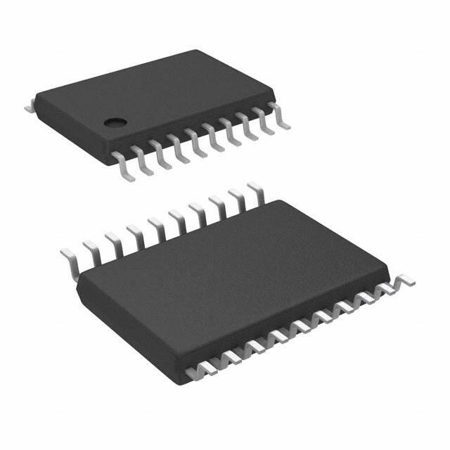


 工商网监
湘ICP备2023018690号
工商网监
湘ICP备2023018690号
