C8051F91x-C8051F90x
Single/Dual Battery, 0.9–3.6 V, 16–8 kB, SmaRTClock, 12/10-Bit ADC MCU
Ultra-Low Power
- 160 uA/MHz in active mode (24.5 MHz clock)
- 2 us wake-up time (two-cell mode)
- 10 nA sleep mode with memory retention;
- 50 nA sleep mode with brownout detector
- 300 nA sleep mode with LFO (‘F912/02 only)
- 600 nA sleep mode with external crystal
Supply Voltage 0.9 to 3.6 V
- One-cell mode supports 0.9 to 1.8 V operation
High-Speed 8051 µC Core
- Pipelined instruction architecture; executes 70% of
instructions in 1 or 2 system clocks
- Up to 25 MIPS throughput with 25 MHz clock
- Expanded interrupt handler
Memory
- 768 bytes RAM
- 16 kB (‘F912/1), or 8 kB (‘F902/1) Flash; In-system
programmable
Two Comparators
- Programmable hysteresis and response time
- Configurable as wake-up or reset source
- Up to 15 Capacitive Touch Sense Inputs
6-Bit Programmable Current Reference
- Up to ±500 µA. Can be used as a bias or for
-
generating a custom reference voltage
PWM enhanced mode on ‘F912/02 devices
ANALOG
PERIPHERALS
A
M
U
X
12/10-bit
75/300 ksps
ADC
TEMP
SENSOR
VREF
VREG
IREF
+
+
–
–
VOLTAGE
COMPARATORS
Digital Peripherals
- 16 port I/O; All 5 V tolerant with high sink
current and programmable drive strength
Hardware SMBus™ (I2C™ Compatible), 2 x SPI™,
and UART serial ports available concurrently
Four general purpose 16-bit counter/timers
Programmable 16-bit counter/timer array with six
capture/compare modules and watchdog timer
-
Clock Sources
- Internal oscillators: 24.5 MHz, 2% accuracy
supports UART operation; 20 MHz low power
oscillator requires very little bias current.
External oscillator: Crystal, RC, C, or CMOS clock
SmaRTClock oscillator: 32 kHz crystal or internal
low frequency oscillator (‘F912/02) or self-oscillate
mode
Can switch between clock sources on-the-fly; useful
in implementing various power saving modes
-
On-Chip Debug
- On-chip debug circuitry facilitates full-speed, nonintrusive in-system debug (no emulator required)
- Provides 4 breakpoints, single stepping
- Inspect/modify memory and registers
- Complete development kit
Packages
- 24-pin QFN (4 x 4 mm)
- 24-pin QSOP (easy to hand-solder)
- Tested die available
Temperature Range: –40 to +85 °C
DIGITAL I/O
UART
SMBus
2 x SPI
PCA
Timer 0
Timer 1
Timer 2
Timer 3
CRC
Port 0
CROSSBAR
(‘F911/01). ‘F912 and ‘F902 devices can operate
from 0.9 to 3.6 V continuously
- Two-cell mode supports 1.8 to 3.6 V operation
- Built-in dc-dc converter with 1.8 to 3.3 V output for
use in one-cell mode
- Built-in LDO regulator allows a high analog supply
voltage and low digital core voltage
- 2 built in supply monitors (brownout detectors)
12-Bit or 10-Bit Analog to Digital Converter
- ±1 LSB INL (10-bit mode); ±1.5 LSB INL (12-bit
mode, ‘F912/02 only) no missing codes
- Programmable throughput up to 300 ksps (10-Bit
Mode) or 75 ksps (12-bit mode, ‘F912/02 only)
- Up to 15 external inputs
- On-chip voltage reference
- On-Chip PGA allows measuring voltages up to twice
the reference voltage
- 16-bit auto-averaging accumulator with burst mode
provides increased ADC resolution
- Data dependent windowed interrupt generator
- Built-in temperature sensor
Port 1
Port 2
24.5 MHz PRECISION
INTERNAL OSCILLATOR
20 MHz LOW POWER
INTERNAL OSCILLATOR
External Oscillator
HARDW ARE SmaRTClock
HIGH-SPEED CONTROLLER CORE
16/8 kB
ISP FLASH
FLEXIBLE
INTERRUPTS
Rev. 1.1 5/11
8051 CPU
(25 MIPS)
DEBUG
CIRCUITRY
768 B SRAM
POR
W DT
Copyright © 2011 by Silicon Laboratories
C8051F91x-C8051F90x
�C8051F91x-C8051F90x
2
Rev. 1.1
�C8051F91x-C8051F90x
Table of Contents
1. System Overview.................................................................................................... 17
1.1. CIP-51™ Microcontroller Core.......................................................................... 20
1.1.1. Fully 8051 Compatible.............................................................................. 20
1.1.2. Improved Throughput ............................................................................... 20
1.1.3. Additional Features .................................................................................. 20
1.2. Port Input/Output............................................................................................... 21
1.3. Serial Ports ....................................................................................................... 22
1.4. Programmable Counter Array ........................................................................... 22
1.5. SAR ADC with 16-bit Auto-Averaging Accumulator and
Autonomous Low Power Burst Mode ............................................................... 23
1.6. Programmable Current Reference (IREF0) ...................................................... 24
1.7. Comparators ..................................................................................................... 24
2. Ordering Information.............................................................................................. 26
3. Pinout and Package Definitions............................................................................ 27
4. Electrical Characteristics....................................................................................... 36
4.1. Absolute Maximum Specifications .................................................................... 36
4.2. Electrical Characteristics................................................................................... 37
5. SAR ADC with 16-bit Auto-Averaging Accumulator and
Autonomous Low Power Burst Mode................................................................... 61
5.1. Output Code Formatting ................................................................................... 62
5.2. Modes of Operation .......................................................................................... 63
5.2.1. Starting a Conversion............................................................................... 63
5.2.2. Tracking Modes........................................................................................ 64
5.2.3. Burst Mode ............................................................................................... 65
5.2.4. Settling Time Requirements ..................................................................... 66
5.2.5. Gain Setting.............................................................................................. 67
5.3. 8-Bit Mode......................................................................................................... 67
5.4. 12-Bit Mode (C8051F912/02 Only) ................................................................... 67
5.5. Low Power Mode (C8051F912/902 only) ......................................................... 67
5.6. Programmable Window Detector ...................................................................... 75
5.6.1. Window Detector In Single-Ended Mode ................................................. 77
5.6.2. ADC0 Specifications................................................................................. 77
5.7. ADC0 Analog Multiplexer.................................................................................. 78
5.8. Temperature Sensor ......................................................................................... 80
5.8.1. Calibration ................................................................................................ 81
5.9. Voltage and Ground Reference Options........................................................... 83
5.10.External Voltage References............................................................................ 84
5.11.Internal Voltage References ............................................................................. 84
5.12.Analog Ground Reference................................................................................ 84
5.13.Temperature Sensor Enable ............................................................................ 84
5.14.Voltage Reference Electrical Specifications ..................................................... 85
6. Programmable Current Reference (IREF0) .......................................................... 86
6.1. PWM Enhanced Mode ...................................................................................... 86
Rev. 1.1
3
�C8051F91x-C8051F90x
6.2. IREF0 Specifications......................................................................................... 87
7. Comparators ........................................................................................................... 88
7.1. Comparator Inputs ............................................................................................ 88
7.2. Comparator Outputs ......................................................................................... 89
7.3. Comparator Response Time............................................................................. 90
7.4. Comparator Hysteresis ..................................................................................... 90
7.5. Comparator Register Descriptions.................................................................... 91
7.6. Comparator0 and Comparator1 Analog Multiplexers........................................ 95
8. CIP-51 Microcontroller ........................................................................................... 98
8.1. Performance ..................................................................................................... 98
8.2. Programming and Debugging Support ............................................................. 99
8.3. Instruction Set ................................................................................................... 99
8.3.1. Instruction and CPU Timing ..................................................................... 99
8.4. CIP-51 Register Descriptions.......................................................................... 104
9. Memory Organization........................................................................................... 107
9.1. Program Memory ............................................................................................ 108
9.1.1. MOVX Instruction and Program Memory ............................................... 108
9.2. Data Memory .................................................................................................. 108
9.2.1. Internal RAM .......................................................................................... 108
9.2.2. External RAM ......................................................................................... 110
10. On-Chip XRAM...................................................................................................... 111
10.1.Accessing XRAM............................................................................................ 111
10.1.1.16-Bit MOVX Example ........................................................................... 111
10.1.2.8-Bit MOVX Example ............................................................................. 111
10.2.Special Function Registers............................................................................. 112
11. Special Function Registers ................................................................................. 113
11.1.SFR Paging .................................................................................................... 114
12. Interrupt Handler .................................................................................................. 120
12.1.Enabling Interrupt Sources ............................................................................. 120
12.2.MCU Interrupt Sources and Vectors............................................................... 120
12.3.Interrupt Priorities ........................................................................................... 121
12.4.Interrupt Latency............................................................................................. 121
12.5.Interrupt Register Descriptions ....................................................................... 123
12.6.External Interrupts INT0 and INT1.................................................................. 130
13. Flash Memory ....................................................................................................... 132
13.1.Programming The Flash Memory ................................................................... 132
13.1.1.Flash Lock and Key Functions ............................................................... 132
13.1.2.Flash Erase Procedure .......................................................................... 133
13.1.3.Flash Write Procedure ........................................................................... 133
13.2.Non-volatile Data Storage .............................................................................. 133
13.3.Security Options ............................................................................................. 134
13.4.Determining the Device Part Number at Run Time ........................................ 136
13.5.Flash Write and Erase Guidelines .................................................................. 137
13.5.1.VDD Maintenance and the VDD Monitor ............................................... 137
13.5.2.PSWE Maintenance ............................................................................... 138
4
Rev. 1.1
�C8051F91x-C8051F90x
13.5.3.System Clock ......................................................................................... 138
13.6.Minimizing Flash Read Current ...................................................................... 139
14. Power Management.............................................................................................. 143
14.1.Normal Mode .................................................................................................. 144
14.2.Idle Mode........................................................................................................ 145
14.3.Stop Mode ...................................................................................................... 145
14.4.Suspend Mode ............................................................................................... 146
14.5.Sleep Mode .................................................................................................... 146
14.6.Configuring Wakeup Sources......................................................................... 147
14.7.Determining the Event that Caused the Last Wakeup.................................... 148
14.8.Power Management Specifications ................................................................ 151
15. Cyclic Redundancy Check Unit (CRC0) ............................................................. 152
15.1.CRC Algorithm................................................................................................ 152
15.2.Preparing for a CRC Calculation .................................................................... 154
15.3.Performing a CRC Calculation ....................................................................... 154
15.4.Accessing the CRC0 Result ........................................................................... 154
15.5.CRC0 Bit Reverse Feature............................................................................. 159
16. On-Chip DC-DC Converter (DC0) ........................................................................ 160
16.1.Startup Behavior............................................................................................. 161
16.2.High Power Applications ............................................................................. 162
16.3.Pulse Skipping Mode...................................................................................... 162
16.4.Enabling the DC-DC Converter ...................................................................... 163
16.5.Minimizing Power Supply Noise ..................................................................... 164
16.6.Selecting the Optimum Switch Size................................................................ 164
16.7.DC-DC Converter Clocking Options ............................................................... 164
16.8.DC-DC Converter Behavior in Sleep Mode .................................................... 164
16.9.Bypass Mode (C8051F912/02 only) ............................................................... 165
16.10.Low Power Mode (C8051F912/02 only) ....................................................... 165
16.11.Passive Diode Mode (C8051F912/02 only).................................................. 166
16.12.DC-DC Converter Register Descriptions ...................................................... 167
16.13.DC-DC Converter Specifications .................................................................. 169
17. Voltage Regulator (VREG0) ................................................................................. 170
17.1.Voltage Regulator Electrical Specifications .................................................... 170
18. Reset Sources....................................................................................................... 171
18.1.Power-On (VBAT Supply Monitor) Reset ....................................................... 172
18.2.Power-Fail (VDD/DC+ Supply Monitor) Reset................................................ 173
18.3.External Reset ................................................................................................ 176
18.4.Missing Clock Detector Reset ........................................................................ 176
18.5.Comparator0 Reset ........................................................................................ 176
18.6.PCA Watchdog Timer Reset .......................................................................... 176
18.7.Flash Error Reset ........................................................................................... 177
18.8.SmaRTClock (Real Time Clock) Reset .......................................................... 177
18.9.Software Reset ............................................................................................... 177
19. Clocking Sources ................................................................................................. 179
19.1.Programmable Precision Internal Oscillator ................................................... 180
Rev. 1.1
5
�C8051F91x-C8051F90x
19.2.Low Power Internal Oscillator......................................................................... 180
19.3.External Oscillator Drive Circuit...................................................................... 180
19.3.1.External Crystal Mode............................................................................ 180
19.3.2.External RC Mode.................................................................................. 182
19.3.3.External Capacitor Mode........................................................................ 183
19.3.4.External CMOS Clock Mode .................................................................. 184
19.4.Special Function Registers for Selecting and Configuring the System Clock 185
20. SmaRTClock (Real Time Clock) .......................................................................... 188
20.1.SmaRTClock Interface ................................................................................... 189
20.1.1.SmaRTClock Lock and Key Functions................................................... 189
20.1.2.Using RTC0ADR and RTC0DAT to Access SmaRTClock
Internal Registers ................................................................................... 190
20.1.3.RTC0ADR Short Strobe Feature............................................................ 190
20.1.4.SmaRTClock Interface Autoread Feature .............................................. 190
20.1.5.RTC0ADR Autoincrement Feature......................................................... 191
20.2.SmaRTClock Clocking Sources ..................................................................... 194
20.2.1.Using the SmaRTClock Oscillator with a Crystal or
External CMOS Clock ............................................................................ 194
20.2.2.Using the SmaRTClock Oscillator in Self-Oscillate Mode...................... 195
20.2.3.Using the Low Frequency Oscillator (LFO) ............................................ 195
20.2.4.Programmable Load Capacitance.......................................................... 196
20.2.5.Automatic Gain Control (Crystal Mode Only) and
SmaRTClock Bias Doubling ................................................................... 197
20.2.6.Missing SmaRTClock Detector .............................................................. 199
20.2.7.SmaRTClock Oscillator Crystal Valid Detector ...................................... 199
20.3.SmaRTClock Timer and Alarm Function ........................................................ 199
20.3.1.Setting and Reading the SmaRTClock Timer Value .............................. 199
20.3.2.Setting a SmaRTClock Alarm ................................................................ 200
20.3.3.Software Considerations for using the SmaRTClock Timer and Alarm . 200
21. Port Input/Output.................................................................................................. 205
21.1.Port I/O Modes of Operation........................................................................... 206
21.1.1.Port Pins Configured for Analog I/O....................................................... 206
21.1.2.Port Pins Configured For Digital I/O....................................................... 206
21.1.3.Interfacing Port I/O to 5 V and 3.3 V Logic............................................. 207
21.1.4.Increasing Port I/O Drive Strength ......................................................... 207
21.2.Assigning Port I/O Pins to Analog and Digital Functions................................ 207
21.2.1.Assigning Port I/O Pins to Analog Functions ......................................... 207
21.2.2.Assigning Port I/O Pins to Digital Functions........................................... 208
21.2.3.Assigning Port I/O Pins to External Digital Event Capture Functions .... 208
21.3.Priority Crossbar Decoder .............................................................................. 209
21.4.Port Match ...................................................................................................... 215
21.5.Special Function Registers for Accessing and Configuring Port I/O .............. 217
22. SMBus ................................................................................................................... 225
22.1.Supporting Documents ................................................................................... 226
22.2.SMBus Configuration...................................................................................... 226
6
Rev. 1.1
�C8051F91x-C8051F90x
22.3.SMBus Operation ........................................................................................... 227
22.3.1.Transmitter Vs. Receiver........................................................................ 227
22.3.2.Arbitration............................................................................................... 227
22.3.3.Clock Low Extension.............................................................................. 228
22.3.4.SCL Low Timeout................................................................................... 228
22.3.5.SCL High (SMBus Free) Timeout .......................................................... 228
22.4.Using the SMBus............................................................................................ 229
22.4.1.SMBus Configuration Register............................................................... 230
22.4.2.SMB0CN Control Register ..................................................................... 233
22.4.3.Hardware Slave Address Recognition ................................................... 236
22.4.4.Data Register ......................................................................................... 238
22.5.SMBus Transfer Modes.................................................................................. 239
22.5.1.Write Sequence (Master) ....................................................................... 239
22.5.2.Read Sequence (Master) ....................................................................... 240
22.5.3.Write Sequence (Slave) ......................................................................... 241
22.5.4.Read Sequence (Slave) ......................................................................... 242
22.6.SMBus Status Decoding................................................................................. 242
23. UART0.................................................................................................................... 247
23.1.Enhanced Baud Rate Generation................................................................... 248
23.2.Operational Modes ......................................................................................... 249
23.2.1.8-Bit UART ............................................................................................. 249
23.2.2.9-Bit UART ............................................................................................. 250
23.3.Multiprocessor Communications .................................................................... 250
24. Enhanced Serial Peripheral Interface (SPI0 and SPI1)...................................... 255
24.1.Signal Descriptions......................................................................................... 256
24.1.1.Master Out, Slave In (MOSI).................................................................. 256
24.1.2.Master In, Slave Out (MISO).................................................................. 256
24.1.3.Serial Clock (SCK) ................................................................................. 256
24.1.4.Slave Select (NSS) ................................................................................ 256
24.2.SPI Master Mode Operation ........................................................................... 257
24.3.SPI Slave Mode Operation ............................................................................. 259
24.4.SPI Interrupt Sources ..................................................................................... 259
24.5.Serial Clock Phase and Polarity ..................................................................... 260
24.6.SPI Special Function Registers ...................................................................... 262
25. Timers.................................................................................................................... 270
25.1.Timer 0 and Timer 1 ....................................................................................... 272
25.1.1.Mode 0: 13-bit Counter/Timer ................................................................ 272
25.1.2.Mode 1: 16-bit Counter/Timer ................................................................ 273
25.1.3.Mode 2: 8-bit Counter/Timer with Auto-Reload...................................... 274
25.1.4.Mode 3: Two 8-bit Counter/Timers (Timer 0 Only)................................. 275
25.2.Timer 2 .......................................................................................................... 280
25.2.1.16-bit Timer with Auto-Reload................................................................ 280
25.2.2.8-bit Timers with Auto-Reload................................................................ 281
25.2.3.Comparator 0/SmaRTClock Capture Mode ........................................... 282
25.3.Timer 3 .......................................................................................................... 286
Rev. 1.1
7
�C8051F91x-C8051F90x
25.3.1.16-bit Timer with Auto-Reload................................................................ 286
25.3.2.8-bit Timers with Auto-Reload................................................................ 287
25.3.3.Comparator 1/External Oscillator Capture Mode ................................... 288
26. Programmable Counter Array ............................................................................. 292
26.1.PCA Counter/Timer ........................................................................................ 293
26.2.PCA0 Interrupt Sources.................................................................................. 294
26.3.Capture/Compare Modules ............................................................................ 296
26.3.1.Edge-triggered Capture Mode................................................................ 297
26.3.2.Software Timer (Compare) Mode........................................................... 298
26.3.3.High-Speed Output Mode ...................................................................... 299
26.3.4.Frequency Output Mode ........................................................................ 300
26.3.5. 8-Bit, 9-Bit, 10-Bit and 11-Bit Pulse Width Modulator Modes............... 301
26.3.6. 16-Bit Pulse Width Modulator Mode..................................................... 303
26.4.Watchdog Timer Mode ................................................................................... 304
26.4.1.Watchdog Timer Operation .................................................................... 304
26.4.2.Watchdog Timer Usage ......................................................................... 305
26.5.Register Descriptions for PCA0...................................................................... 306
27. C2 Interface ........................................................................................................... 312
27.1.C2 Interface Registers.................................................................................... 312
27.2.C2 Pin Sharing ............................................................................................... 315
Document Change List............................................................................................. 316
Contact Information.................................................................................................. 318
8
Rev. 1.1
�C8051F91x-C8051F90x
List of Figures
Figure 1.1. C8051F912 Block Diagram .................................................................... 18
Figure 1.2. C8051F911 Block Diagram .................................................................... 18
Figure 1.3. C8051F902 Block Diagram .................................................................... 19
Figure 1.4. C8051F901 Block Diagram .................................................................... 19
Figure 1.5. Port I/O Functional Block Diagram ......................................................... 21
Figure 1.6. PCA Block Diagram................................................................................ 22
Figure 1.7. ADC0 Functional Block Diagram............................................................ 23
Figure 1.8. ADC0 Multiplexer Block Diagram ........................................................... 24
Figure 1.9. Comparator 0 Functional Block Diagram ............................................... 25
Figure 1.10. Comparator 1 Functional Block Diagram ............................................. 25
Figure 3.1. QFN-24 Pinout Diagram (Top View) ...................................................... 30
Figure 3.2. QSOP-24 Pinout Diagram F912 (Top View) .......................................... 31
Figure 3.3. QFN-24 Package Drawing ..................................................................... 32
Figure 3.4. Typical QFN-24 Landing Diagram.......................................................... 33
Figure 3.5. QSOP-24 Package Diagram .................................................................. 34
Figure 3.6. QSOP-24 Landing Diagram ................................................................... 35
Figure 4.1. Active Mode Current (External CMOS Clock) ........................................ 41
Figure 4.2. Idle Mode Current (External CMOS Clock) ............................................ 42
Figure 4.3. Typical DC-DC Converter Efficiency (High Current, VDD/DC+ = 2 V) ... 43
Figure 4.4. Typical DC-DC Converter Efficiency (High Current, VDD/DC+ = 3 V) ... 44
Figure 4.5. Typical DC-DC Converter Efficiency (Low Current, VDD/DC+ = 2 V).... 45
Figure 4.6. Typical One-Cell Suspend Mode Current............................................... 46
Figure 4.7. Typical VOH Curves, 1.8–3.6 V ............................................................. 48
Figure 4.8. Typical VOH Curves, 0.9–1.8 V ............................................................. 49
Figure 4.9. Typical VOL Curves, 1.8–3.6 V .............................................................. 50
Figure 4.10. Typical VOL Curves, 0.9–1.8 V ............................................................ 51
Figure 5.1. ADC0 Functional Block Diagram............................................................ 61
Figure 5.2. 10-Bit ADC Track and Conversion Example Timing (BURSTEN = 0).... 64
Figure 5.3. Burst Mode Tracking Example with Repeat Count Set to 4 ................... 65
Figure 5.4. ADC0 Equivalent Input Circuits .............................................................. 66
Figure 5.5. ADC Window Compare Example: Right-Justified Single-Ended Data ... 77
Figure 5.6. ADC Window Compare Example: Left-Justified Single-Ended Data...... 77
Figure 5.7. ADC0 Multiplexer Block Diagram ........................................................... 78
Figure 5.8. Temperature Sensor Transfer Function ................................................. 80
Figure 5.9. Temperature Sensor Error with 1-Point Calibration (VREF = 1.68 V) ..... 81
Figure 5.10. Voltage Reference Functional Block Diagram...................................... 83
Figure 7.1. Comparator 0 Functional Block Diagram ............................................... 88
Figure 7.2. Comparator 1 Functional Block Diagram ............................................... 89
Figure 7.3. Comparator Hysteresis Plot ................................................................... 90
Figure 7.4. CPn Multiplexer Block Diagram.............................................................. 95
Figure 8.1. CIP-51 Block Diagram............................................................................ 98
Figure 9.1. C8051F91x-C8051F90x Memory Map ................................................. 107
Figure 9.2. Flash Program Memory Map................................................................ 108
Rev. 1.1
9
�C8051F91x-C8051F90x
Figure 13.1. Flash Program Memory Map (16 kB and 8 kB devices)..................... 134
Figure 14.1. C8051F91x-C8051F90x Power Distribution....................................... 144
Figure 15.1. CRC0 Block Diagram ......................................................................... 152
Figure 15.2. Bit Reverse Register .......................................................................... 159
Figure 16.1. DC-DC Converter Block Diagram....................................................... 160
Figure 16.2. DC-DC Converter Configuration Options ........................................... 163
Figure 18.1. Reset Sources.................................................................................... 171
Figure 18.2. Power-Fail Reset Timing Diagram ..................................................... 172
Figure 18.3. Power-Fail Reset Timing Diagram ..................................................... 173
Figure 19.1. Clocking Sources Block Diagram ....................................................... 179
Figure 19.2. 25 MHz External Crystal Example...................................................... 181
Figure 20.1. SmaRTClock Block Diagram.............................................................. 188
Figure 20.2. Interpreting Oscillation Robustness (Duty Cycle) Test Results.......... 197
Figure 21.1. Port I/O Functional Block Diagram ..................................................... 205
Figure 21.2. Port I/O Cell Block Diagram ............................................................... 206
Figure 21.3. Crossbar Priority Decoder with No Pins Skipped ............................... 210
Figure 21.4. Crossbar Priority Decoder with Crystal Pins Skipped ........................ 211
Figure 22.1. SMBus Block Diagram ....................................................................... 225
Figure 22.2. Typical SMBus Configuration ............................................................. 226
Figure 22.3. SMBus Transaction ............................................................................ 227
Figure 22.4. Typical SMBus SCL Generation......................................................... 230
Figure 22.5. Typical Master Write Sequence ......................................................... 239
Figure 22.6. Typical Master Read Sequence ......................................................... 240
Figure 22.7. Typical Slave Write Sequence ........................................................... 241
Figure 22.8. Typical Slave Read Sequence ........................................................... 242
Figure 23.1. UART0 Block Diagram ....................................................................... 247
Figure 23.2. UART0 Baud Rate Logic .................................................................... 248
Figure 23.3. UART Interconnect Diagram .............................................................. 249
Figure 23.4. 8-Bit UART Timing Diagram............................................................... 249
Figure 23.5. 9-Bit UART Timing Diagram............................................................... 250
Figure 23.6. UART Multi-Processor Mode Interconnect Diagram .......................... 251
Figure 24.1. SPI Block Diagram ............................................................................. 255
Figure 24.2. Multiple-Master Mode Connection Diagram ....................................... 258
Figure 24.3. 3-Wire Single Master and 3-Wire Single Slave Mode
Connection Diagram ........................................................................... 258
Figure 24.4. 4-Wire Single Master Mode and 4-Wire Slave Mode
Connection Diagram........................................................................... 258
Figure 24.5. Master Mode Data/Clock Timing ........................................................ 260
Figure 24.6. Slave Mode Data/Clock Timing (CKPHA = 0) .................................... 261
Figure 24.7. Slave Mode Data/Clock Timing (CKPHA = 1) .................................... 261
Figure 24.8. SPI Master Timing (CKPHA = 0)........................................................ 267
Figure 24.9. SPI Master Timing (CKPHA = 1)........................................................ 267
Figure 24.10. SPI Slave Timing (CKPHA = 0)........................................................ 268
Figure 24.11. SPI Slave Timing (CKPHA = 1)........................................................ 268
Figure 25.1. T0 Mode 0 Block Diagram.................................................................. 273
10
Rev. 1.1
�C8051F91x-C8051F90x
Figure 25.2. T0 Mode 2 Block Diagram.................................................................. 274
Figure 25.3. T0 Mode 3 Block Diagram.................................................................. 275
Figure 25.4. Timer 2 16-Bit Mode Block Diagram .................................................. 280
Figure 25.5. Timer 2 8-Bit Mode Block Diagram .................................................... 281
Figure 25.6. Timer 2 Capture Mode Block Diagram ............................................... 282
Figure 25.7. Timer 3 16-Bit Mode Block Diagram .................................................. 286
Figure 25.8. Timer 3 8-Bit Mode Block Diagram. ................................................... 287
Figure 25.9. Timer 3 Capture Mode Block Diagram ............................................... 288
Figure 26.1. PCA Block Diagram............................................................................ 292
Figure 26.2. PCA Counter/Timer Block Diagram.................................................... 294
Figure 26.3. PCA Interrupt Block Diagram ............................................................. 295
Figure 26.4. PCA Capture Mode Diagram.............................................................. 297
Figure 26.5. PCA Software Timer Mode Diagram .................................................. 298
Figure 26.6. PCA High-Speed Output Mode Diagram............................................ 299
Figure 26.7. PCA Frequency Output Mode ............................................................ 300
Figure 26.8. PCA 8-Bit PWM Mode Diagram ......................................................... 301
Figure 26.9. PCA 9, 10 and 11-Bit PWM Mode Diagram ....................................... 302
Figure 26.10. PCA 16-Bit PWM Mode.................................................................... 303
Figure 26.11. PCA Module 5 with Watchdog Timer Enabled ................................. 304
Figure 27.1. Typical C2 Pin Sharing....................................................................... 315
Rev. 1.1
11
�C8051F91x-C8051F90x
List of Tables
2. . . . . . . . . . . . . . . . . . . . . . . . . . . . . . . . . . . . . . . . . . . . . . . . . . . . . . . . . . . . . . . . 26
Table 2.1. Product Selection Guide . . . . . . . . . . . . . . . . . . . . . . . . . . . . . . . . . . . . 26
Table 3.1. Pin Definitions for the C8051F91x-C8051F90x . . . . . . . . . . . . . . . . . . . 27
Table 3.2. QFN-24 Package Dimensions . . . . . . . . . . . . . . . . . . . . . . . . . . . . . . . . 32
Table 3.3. PCB Land Pattern ................................................................................... 33
Table 3.4. QSOP-24 Package Dimensions ............................................................. 34
Table 3.5. PCB Land Pattern . . . . . . . . . . . . . . . . . . . . . . . . . . . . . . . . . . . . . . . . . . 35
Table 4.1. Absolute Maximum Ratings .................................................................... 36
Table 4.2. Global Electrical Characteristics ............................................................. 37
Table 4.3. Port I/O DC Electrical Characteristics ..................................................... 47
Table 4.4. Reset Electrical Characteristics .............................................................. 52
Table 4.5. Power Management Electrical Specifications ......................................... 53
Table 4.6. Flash Electrical Characteristics .............................................................. 53
Table 4.7. Internal Precision Oscillator Electrical Characteristics ........................... 53
Table 4.8. Internal Low-Power Oscillator Electrical Characteristics ........................ 53
Table 4.9. SmaRTClock Characteristics .................................................................. 54
Table 4.10. ADC0 Electrical Characteristics ............................................................ 54
Table 4.11. Temperature Sensor Electrical Characteristics .................................... 55
Table 4.12. Voltage Reference Electrical Characteristics ....................................... 56
Table 4.13. IREF0 Electrical Characteristics ........................................................... 57
Table 4.14. Comparator Electrical Characteristics .................................................. 58
Table 4.15. VREG0 Electrical Characteristics ......................................................... 59
Table 4.16. DC-DC Converter (DC0) Electrical Characteristics .............................. 60
Table 5.1. Representative Conversion Times and Energy Consumption for the SAR
ADC with 1.65 V High-Speed VREF . . . . . . . . . . . . . . . . . . . . . . . . . . . . 68
Table 8.1. CIP-51 Instruction Set Summary . . . . . . . . . . . . . . . . . . . . . . . . . . . . . 100
Table 11.1. Special Function Register (SFR) Memory Map (Page 0x0) . . . . . . . . 113
Table 11.2. Special Function Register (SFR) Memory Map (Page 0xF) . . . . . . . . 114
Table 11.3. Special Function Registers . . . . . . . . . . . . . . . . . . . . . . . . . . . . . . . . . 115
Table 12.1. Interrupt Summary . . . . . . . . . . . . . . . . . . . . . . . . . . . . . . . . . . . . . . . 122
Table 13.1. Flash Security Summary . . . . . . . . . . . . . . . . . . . . . . . . . . . . . . . . . . 135
Table 14.1. Power Modes . . . . . . . . . . . . . . . . . . . . . . . . . . . . . . . . . . . . . . . . . . . 143
Table 15.1. Example 16-bit CRC Outputs . . . . . . . . . . . . . . . . . . . . . . . . . . . . . . . 153
Table 16.1. IPeak Inductor Current Limit Settings . . . . . . . . . . . . . . . . . . . . . . . . . 161
Table 19.1. Recommended XFCN Settings for Crystal Mode . . . . . . . . . . . . . . . . 181
Table 19.2. Recommended XFCN Settings for RC and C modes . . . . . . . . . . . . . 182
Table 20.1. SmaRTClock Internal Registers ......................................................... 189
Table 20.2. SmaRTClock Load Capacitance Settings . . . . . . . . . . . . . . . . . . . . . 196
Table 20.3. SmaRTClock Bias Settings . . . . . . . . . . . . . . . . . . . . . . . . . . . . . . . . 198
Table 21.1. Port I/O Assignment for Analog Functions . . . . . . . . . . . . . . . . . . . . . 207
Table 21.2. Port I/O Assignment for Digital Functions . . . . . . . . . . . . . . . . . . . . . . 208
Table 21.3. Port I/O Assignment for External Digital Event Capture Functions . . 208
Table 22.1. SMBus Clock Source Selection . . . . . . . . . . . . . . . . . . . . . . . . . . . . . 230
12
Rev. 1.1
�C8051F91x-C8051F90x
Table 22.2. Minimum SDA Setup and Hold Times . . . . . . . . . . . . . . . . . . . . . . . . 231
Table 22.3. Sources for Hardware Changes to SMB0CN . . . . . . . . . . . . . . . . . . . 235
Table 22.4. Hardware Address Recognition Examples (EHACK = 1) . . . . . . . . . . 236
Table 22.5. SMBus Status Decoding With Hardware ACK Generation Disabled
(EHACK = 0) . . . . . . . . . . . . . . . . . . . . . . . . . . . . . . . . . . . . . . . . . . . . 243
Table 22.6. SMBus Status Decoding With Hardware ACK Generation Enabled
(EHACK = 1) . . . . . . . . . . . . . . . . . . . . . . . . . . . . . . . . . . . . . . . . . . . . 245
Table 23.1. Timer Settings for Standard Baud Rates
Using The Internal 24.5 MHz Oscillator . . . . . . . . . . . . . . . . . . . . . . . 254
Table 23.2. Timer Settings for Standard Baud Rates
Using an External 22.1184 MHz Oscillator . . . . . . . . . . . . . . . . . . . . . 254
Table 24.1. SPI Slave Timing Parameters . . . . . . . . . . . . . . . . . . . . . . . . . . . . . . 269
Table 25.1. Timer 0 Running Modes . . . . . . . . . . . . . . . . . . . . . . . . . . . . . . . . . . . 272
Table 26.1. PCA Timebase Input Options . . . . . . . . . . . . . . . . . . . . . . . . . . . . . . . 293
Table 26.2. PCA0CPM and PCA0PWM Bit Settings for PCA
Capture/Compare Modules . . . . . . . . . . . . . . . . . . . . . . . . . . . . . . . . 296
Table 26.3. Watchdog Timer Timeout Intervals . . . . . . . . . . . . . . . . . . . . . . . . . . . 305
Rev. 1.1
13
�C8051F91x-C8051F90x
List of Registers
SFR Definition 5.1. ADC0CN: ADC0 Control . . . . . . . . . . . . . . . . . . . . . . . . . . . . . . . . 69
SFR Definition 5.2. ADC0CF: ADC0 Configuration . . . . . . . . . . . . . . . . . . . . . . . . . . . 70
SFR Definition 5.3. ADC0AC: ADC0 Accumulator Configuration . . . . . . . . . . . . . . . . . 71
SFR Definition 5.4. ADC0PWR: ADC0 Burst Mode Power-Up Time . . . . . . . . . . . . . . 72
SFR Definition 5.5. ADC0TK: ADC0 Burst Mode Track Time . . . . . . . . . . . . . . . . . . . . 73
SFR Definition 5.6. ADC0H: ADC0 Data Word High Byte . . . . . . . . . . . . . . . . . . . . . . 74
SFR Definition 5.7. ADC0L: ADC0 Data Word Low Byte . . . . . . . . . . . . . . . . . . . . . . . 74
SFR Definition 5.8. ADC0GTH: ADC0 Greater-Than High Byte . . . . . . . . . . . . . . . . . . 75
SFR Definition 5.9. ADC0GTL: ADC0 Greater-Than Low Byte . . . . . . . . . . . . . . . . . . 75
SFR Definition 5.10. ADC0LTH: ADC0 Less-Than High Byte . . . . . . . . . . . . . . . . . . . 76
SFR Definition 5.11. ADC0LTL: ADC0 Less-Than Low Byte . . . . . . . . . . . . . . . . . . . . 76
SFR Definition 5.12. ADC0MX: ADC0 Input Channel Select . . . . . . . . . . . . . . . . . . . . 79
SFR Definition 5.13. TOFFH: ADC0 Data Word High Byte . . . . . . . . . . . . . . . . . . . . . 82
SFR Definition 5.14. TOFFL: ADC0 Data Word Low Byte . . . . . . . . . . . . . . . . . . . . . . 82
SFR Definition 5.15. REF0CN: Voltage Reference Control . . . . . . . . . . . . . . . . . . . . . 85
SFR Definition 6.1. IREF0CN: Current Reference Control . . . . . . . . . . . . . . . . . . . . . . 86
SFR Definition 6.2. IREF0CF: Current Reference Configuration . . . . . . . . . . . . . . . . . 87
SFR Definition 7.1. CPT0CN: Comparator 0 Control . . . . . . . . . . . . . . . . . . . . . . . . . . 91
SFR Definition 7.2. CPT0MD: Comparator 0 Mode Selection . . . . . . . . . . . . . . . . . . . 92
SFR Definition 7.3. CPT1CN: Comparator 1 Control . . . . . . . . . . . . . . . . . . . . . . . . . . 93
SFR Definition 7.4. CPT1MD: Comparator 1 Mode Selection . . . . . . . . . . . . . . . . . . . 94
SFR Definition 7.5. CPT0MX: Comparator0 Input Channel Select . . . . . . . . . . . . . . . . 96
SFR Definition 7.6. CPT1MX: Comparator1 Input Channel Select . . . . . . . . . . . . . . . . 97
SFR Definition 8.1. DPL: Data Pointer Low Byte . . . . . . . . . . . . . . . . . . . . . . . . . . . . 104
SFR Definition 8.2. DPH: Data Pointer High Byte . . . . . . . . . . . . . . . . . . . . . . . . . . . . 104
SFR Definition 8.3. SP: Stack Pointer . . . . . . . . . . . . . . . . . . . . . . . . . . . . . . . . . . . . . 105
SFR Definition 8.4. ACC: Accumulator . . . . . . . . . . . . . . . . . . . . . . . . . . . . . . . . . . . . 105
SFR Definition 8.5. B: B Register . . . . . . . . . . . . . . . . . . . . . . . . . . . . . . . . . . . . . . . . 105
SFR Definition 8.6. PSW: Program Status Word . . . . . . . . . . . . . . . . . . . . . . . . . . . . 106
SFR Definition 10.1. EMI0CN: External Memory Interface Control . . . . . . . . . . . . . . 112
SFR Definition 11.1. SFR Page: SFR Page . . . . . . . . . . . . . . . . . . . . . . . . . . . . . . . . 115
SFR Definition 12.1. IE: Interrupt Enable . . . . . . . . . . . . . . . . . . . . . . . . . . . . . . . . . . 124
SFR Definition 12.2. IP: Interrupt Priority . . . . . . . . . . . . . . . . . . . . . . . . . . . . . . . . . . 125
SFR Definition 12.3. EIE1: Extended Interrupt Enable 1 . . . . . . . . . . . . . . . . . . . . . . 126
SFR Definition 12.4. EIP1: Extended Interrupt Priority 1 . . . . . . . . . . . . . . . . . . . . . . 127
SFR Definition 12.5. EIE2: Extended Interrupt Enable 2 . . . . . . . . . . . . . . . . . . . . . . 128
SFR Definition 12.6. EIP2: Extended Interrupt Priority 2 . . . . . . . . . . . . . . . . . . . . . . 129
SFR Definition 12.7. IT01CF: INT0/INT1 Configuration . . . . . . . . . . . . . . . . . . . . . . . 131
SFR Definition 13.1. PSCTL: Program Store R/W Control . . . . . . . . . . . . . . . . . . . . . 140
SFR Definition 13.2. FLKEY: Flash Lock and Key . . . . . . . . . . . . . . . . . . . . . . . . . . . 141
SFR Definition 13.3. FLSCL: Flash Scale . . . . . . . . . . . . . . . . . . . . . . . . . . . . . . . . . . 142
SFR Definition 13.4. FLWR: Flash Write Only . . . . . . . . . . . . . . . . . . . . . . . . . . . . . . 142
SFR Definition 14.1. PMU0CF: Power Management Unit Configuration1,2 . . . . . . . . 149
14
Rev. 1.1
�C8051F91x-C8051F90x
SFR Definition 14.2. PMU0MD: Power Management Unit Mode . . . . . . . . . . . . . . . . 150
SFR Definition 14.3. PCON: Power Management Control Register . . . . . . . . . . . . . . 151
SFR Definition 15.1. CRC0CN: CRC0 Control . . . . . . . . . . . . . . . . . . . . . . . . . . . . . . 155
SFR Definition 15.2. CRC0IN: CRC0 Data Input . . . . . . . . . . . . . . . . . . . . . . . . . . . . 156
SFR Definition 15.3. CRC0DAT: CRC0 Data Output . . . . . . . . . . . . . . . . . . . . . . . . . 156
SFR Definition 15.4. CRC0AUTO: CRC0 Automatic Control . . . . . . . . . . . . . . . . . . . 157
SFR Definition 15.5. CRC0CNT: CRC0 Automatic Flash Sector Count . . . . . . . . . . . 158
SFR Definition 15.6. CRC0FLIP: CRC0 Bit Flip . . . . . . . . . . . . . . . . . . . . . . . . . . . . . 159
SFR Definition 16.1. DC0CN: DC-DC Converter Control . . . . . . . . . . . . . . . . . . . . . . 167
SFR Definition 16.2. DC0CF: DC-DC Converter Configuration . . . . . . . . . . . . . . . . . 168
SFR Definition 16.3. DC0MD: DC-DC Mode . . . . . . . . . . . . . . . . . . . . . . . . . . . . . . . 169
SFR Definition 17.1. REG0CN: Voltage Regulator Control . . . . . . . . . . . . . . . . . . . . 170
SFR Definition 18.1. VDM0CN: VDD/DC+ Supply Monitor Control . . . . . . . . . . . . . . 175
SFR Definition 18.2. RSTSRC: Reset Source . . . . . . . . . . . . . . . . . . . . . . . . . . . . . . 178
SFR Definition 19.1. CLKSEL: Clock Select . . . . . . . . . . . . . . . . . . . . . . . . . . . . . . . . 185
SFR Definition 19.2. OSCICN: Internal Oscillator Control . . . . . . . . . . . . . . . . . . . . . 186
SFR Definition 19.3. OSCICL: Internal Oscillator Calibration . . . . . . . . . . . . . . . . . . . 186
SFR Definition 19.4. OSCXCN: External Oscillator Control . . . . . . . . . . . . . . . . . . . . 187
SFR Definition 20.1. RTC0KEY: SmaRTClock Lock and Key . . . . . . . . . . . . . . . . . . 192
SFR Definition 20.2. RTC0ADR: SmaRTClock Address . . . . . . . . . . . . . . . . . . . . . . 193
SFR Definition 20.3. RTC0DAT: SmaRTClock Data . . . . . . . . . . . . . . . . . . . . . . . . . 193
Internal Register Definition 20.4. RTC0CN: SmaRTClock Control . . . . . . . . . . . . . . . 201
Internal Register Definition 20.5. RTC0XCN: SmaRTClock Oscillator Control . . . . . . 202
Internal Register Definition 20.6. RTC0XCF: SmaRTClock Oscillator Configuration . 203
Internal Register Definition 20.7. RTC0PIN: SmaRTClock Pin Configuration . . . . . . 203
Internal Register Definition 20.8. CAPTUREn: SmaRTClock Timer Capture . . . . . . . 204
Internal Register Definition 20.9. ALARMn: SmaRTClock Alarm Programmed Value 204
SFR Definition 21.1. XBR0: Port I/O Crossbar Register 0 . . . . . . . . . . . . . . . . . . . . . 212
SFR Definition 21.2. XBR1: Port I/O Crossbar Register 1 . . . . . . . . . . . . . . . . . . . . . 213
SFR Definition 21.3. XBR2: Port I/O Crossbar Register 2 . . . . . . . . . . . . . . . . . . . . . 214
SFR Definition 21.4. P0MASK: Port0 Mask Register . . . . . . . . . . . . . . . . . . . . . . . . . 215
SFR Definition 21.5. P0MAT: Port0 Match Register . . . . . . . . . . . . . . . . . . . . . . . . . . 215
SFR Definition 21.6. P1MASK: Port1 Mask Register . . . . . . . . . . . . . . . . . . . . . . . . . 216
SFR Definition 21.7. P1MAT: Port1 Match Register . . . . . . . . . . . . . . . . . . . . . . . . . . 216
SFR Definition 21.8. P0: Port0 . . . . . . . . . . . . . . . . . . . . . . . . . . . . . . . . . . . . . . . . . . 218
SFR Definition 21.9. P0SKIP: Port0 Skip . . . . . . . . . . . . . . . . . . . . . . . . . . . . . . . . . . 218
SFR Definition 21.10. P0MDIN: Port0 Input Mode . . . . . . . . . . . . . . . . . . . . . . . . . . . 219
SFR Definition 21.11. P0MDOUT: Port0 Output Mode . . . . . . . . . . . . . . . . . . . . . . . . 219
SFR Definition 21.12. P0DRV: Port0 Drive Strength . . . . . . . . . . . . . . . . . . . . . . . . . 220
SFR Definition 21.13. P1: Port1 . . . . . . . . . . . . . . . . . . . . . . . . . . . . . . . . . . . . . . . . . 221
SFR Definition 21.14. P1SKIP: Port1 Skip . . . . . . . . . . . . . . . . . . . . . . . . . . . . . . . . . 221
SFR Definition 21.15. P1MDIN: Port1 Input Mode . . . . . . . . . . . . . . . . . . . . . . . . . . . 222
SFR Definition 21.16. P1MDOUT: Port1 Output Mode . . . . . . . . . . . . . . . . . . . . . . . . 222
SFR Definition 21.17. P1DRV: Port1 Drive Strength . . . . . . . . . . . . . . . . . . . . . . . . . 223
SFR Definition 21.18. P2: Port2 . . . . . . . . . . . . . . . . . . . . . . . . . . . . . . . . . . . . . . . . . 223
Rev. 1.1
15
�C8051F91x-C8051F90x
SFR Definition 21.19. P2MDOUT: Port2 Output Mode . . . . . . . . . . . . . . . . . . . . . . . . 224
SFR Definition 21.20. P2DRV: Port2 Drive Strength . . . . . . . . . . . . . . . . . . . . . . . . . 224
SFR Definition 22.1. SMB0CF: SMBus Clock/Configuration . . . . . . . . . . . . . . . . . . . 232
SFR Definition 22.2. SMB0CN: SMBus Control . . . . . . . . . . . . . . . . . . . . . . . . . . . . . 234
SFR Definition 22.3. SMB0ADR: SMBus Slave Address . . . . . . . . . . . . . . . . . . . . . . 237
SFR Definition 22.4. SMB0ADM: SMBus Slave Address Mask . . . . . . . . . . . . . . . . . 237
SFR Definition 22.5. SMB0DAT: SMBus Data . . . . . . . . . . . . . . . . . . . . . . . . . . . . . . 238
SFR Definition 23.1. SCON0: Serial Port 0 Control . . . . . . . . . . . . . . . . . . . . . . . . . . 252
SFR Definition 23.2. SBUF0: Serial (UART0) Port Data Buffer . . . . . . . . . . . . . . . . . 253
SFR Definition 24.1. SPInCFG: SPI Configuration . . . . . . . . . . . . . . . . . . . . . . . . . . . 263
SFR Definition 24.2. SPInCN: SPI Control . . . . . . . . . . . . . . . . . . . . . . . . . . . . . . . . . 264
SFR Definition 24.3. SPInCKR: SPI Clock Rate . . . . . . . . . . . . . . . . . . . . . . . . . . . . . 265
SFR Definition 24.4. SPInDAT: SPI Data . . . . . . . . . . . . . . . . . . . . . . . . . . . . . . . . . . 266
SFR Definition 25.1. CKCON: Clock Control . . . . . . . . . . . . . . . . . . . . . . . . . . . . . . . 271
SFR Definition 25.2. TCON: Timer Control . . . . . . . . . . . . . . . . . . . . . . . . . . . . . . . . . 276
SFR Definition 25.3. TMOD: Timer Mode . . . . . . . . . . . . . . . . . . . . . . . . . . . . . . . . . . 277
SFR Definition 25.4. TL0: Timer 0 Low Byte . . . . . . . . . . . . . . . . . . . . . . . . . . . . . . . . 278
SFR Definition 25.5. TL1: Timer 1 Low Byte . . . . . . . . . . . . . . . . . . . . . . . . . . . . . . . . 278
SFR Definition 25.6. TH0: Timer 0 High Byte . . . . . . . . . . . . . . . . . . . . . . . . . . . . . . . 279
SFR Definition 25.7. TH1: Timer 1 High Byte . . . . . . . . . . . . . . . . . . . . . . . . . . . . . . . 279
SFR Definition 25.8. TMR2CN: Timer 2 Control . . . . . . . . . . . . . . . . . . . . . . . . . . . . . 283
SFR Definition 25.9. TMR2RLL: Timer 2 Reload Register Low Byte . . . . . . . . . . . . . 284
SFR Definition 25.10. TMR2RLH: Timer 2 Reload Register High Byte . . . . . . . . . . . 284
SFR Definition 25.11. TMR2L: Timer 2 Low Byte . . . . . . . . . . . . . . . . . . . . . . . . . . . . 285
SFR Definition 25.12. TMR2H Timer 2 High Byte . . . . . . . . . . . . . . . . . . . . . . . . . . . . 285
SFR Definition 25.13. TMR3CN: Timer 3 Control . . . . . . . . . . . . . . . . . . . . . . . . . . . . 289
SFR Definition 25.14. TMR3RLL: Timer 3 Reload Register Low Byte . . . . . . . . . . . . 290
SFR Definition 25.15. TMR3RLH: Timer 3 Reload Register High Byte . . . . . . . . . . . 290
SFR Definition 25.16. TMR3L: Timer 3 Low Byte . . . . . . . . . . . . . . . . . . . . . . . . . . . . 291
SFR Definition 25.17. TMR3H Timer 3 High Byte . . . . . . . . . . . . . . . . . . . . . . . . . . . . 291
SFR Definition 26.1. PCA0CN: PCA Control . . . . . . . . . . . . . . . . . . . . . . . . . . . . . . . 306
SFR Definition 26.2. PCA0MD: PCA Mode . . . . . . . . . . . . . . . . . . . . . . . . . . . . . . . . 307
SFR Definition 26.3. PCA0PWM: PCA PWM Configuration . . . . . . . . . . . . . . . . . . . . 308
SFR Definition 26.4. PCA0CPMn: PCA Capture/Compare Mode . . . . . . . . . . . . . . . 309
SFR Definition 26.5. PCA0L: PCA Counter/Timer Low Byte . . . . . . . . . . . . . . . . . . . 310
SFR Definition 26.6. PCA0H: PCA Counter/Timer High Byte . . . . . . . . . . . . . . . . . . . 310
SFR Definition 26.7. PCA0CPLn: PCA Capture Module Low Byte . . . . . . . . . . . . . . . 311
SFR Definition 26.8. PCA0CPHn: PCA Capture Module High Byte . . . . . . . . . . . . . . 311
C2 Register Definition 27.1. C2ADD: C2 Address . . . . . . . . . . . . . . . . . . . . . . . . . . . 312
C2 Register Definition 27.2. DEVICEID: C2 Device ID . . . . . . . . . . . . . . . . . . . . . . . . 313
C2 Register Definition 27.3. REVID: C2 Revision ID . . . . . . . . . . . . . . . . . . . . . . . . . 313
C2 Register Definition 27.4. FPCTL: C2 Flash Programming Control . . . . . . . . . . . . 314
C2 Register Definition 27.5. FPDAT: C2 Flash Programming Data . . . . . . . . . . . . . . 314
16
Rev. 1.1
�C8051F91x-C8051F90x
1.
System Overview
C8051F91x-C8051F90x devices are fully integrated mixed-signal System-on-a-Chip MCUs. Highlighted
features are listed below. Refer to Table 2.1 for specific product feature selection and part ordering
numbers.
•
•
•
•
•
•
•
•
•
•
•
•
•
•
Single/Dual Battery operation with on-chip dc-dc boost converter.
High-speed pipelined 8051-compatible microcontroller core (up to 25 MIPS)
In-system, full-speed, non-intrusive debug interface (on-chip)
10-bit 300 ksps or 12-bit 75 ksps single-ended ADC with analog multiplexer
6-Bit Programmable Current Reference. Resolution can be increased with PWM.
Precision programmable 24.5 MHz internal oscillator with spread spectrum technology.
16 kB or 8 kB of on-chip Flash memory
768 bytes of on-chip RAM
SMBus/I2C, Enhanced UART, and two Enhanced SPI serial interfaces implemented in hardware
Four general-purpose 16-bit timers
Programmable Counter/Timer Array (PCA) with six capture/compare modules and Watchdog Timer
function
On-chip Power-On Reset, VDD Monitor, and Temperature Sensor
Two On-chip Voltage Comparators with 15 Capacitive Touch Sense inputs.
16 Port I/O (5 V tolerant)
With on-chip Power-On Reset, VDD monitor, Watchdog Timer, and clock oscillator, the C8051F91xC8051F90x devices are truly stand-alone System-on-a-Chip solutions. The Flash memory can be
reprogrammed even in-circuit, providing non-volatile data storage, and also allowing field upgrades of the
8051 firmware. User software has complete control of all peripherals, and may individually shut down any
or all peripherals for power savings.
The on-chip Silicon Labs 2-Wire (C2) Development Interface allows non-intrusive (uses no on-chip
resources), full speed, in-circuit debugging using the production MCU installed in the final application. This
debug logic supports inspection and modification of memory and registers, setting breakpoints, single
stepping, run and halt commands. All analog and digital peripherals are fully functional while debugging
using C2. The two C2 interface pins can be shared with user functions, allowing in-system debugging
without occupying package pins.
Each device is specified for 0.9 to 1.8 V, 0.9 to 3.6 V or 1.8 to 3.6 V operation over the industrial
temperature range (–40 to +85 °C). The Port I/O and RST pins are tolerant of input signals up to 5 V. The
C8051F91x-C8051F90x devices are available in 24-pin QFN or QSOP packages. Both package options
are lead-free and RoHS compliant. See Table 2.1 for ordering information. Block diagrams are included in
Figure 1.1 through Figure 1.4.
Rev. 1.1
17
�C8051F91x-C8051F90x
Wake
Reset
C2CK/RST
Debug /
Programming
Hardware
Power Net
UART
256 Byte SRAM
Timers 0,
1, 2, 3
512 Byte XRAM
VREG
Analog
Power
GND/DC-
DCEN
VBAT
Digital
Power
SPI 0,1
SYSCLK
Crossbar Control
SFR
Bus
XTAL2
XTAL3
XTAL4
P1.0
P1.1
P1.2
P1.3
P1.4
P1.5
P1.6
IREF0
Internal
External
VREF
VREF
Port 2
Drivers
A
M
U
X
12/10-bit
75/300ksps
ADC
SmaRTClock
Oscillator
Port 1
Drivers
P0.0/VREF
P0.1/AGND
P0.2/XTAL1/RTCOUT
P0.3/XTAL2/WAKEOUT
P0.4/TX
P0.5/RX
P0.6/CNVSTR
P0.7/IREF0
Analog Peripherals
6-bit
IREF
External
Oscillator
Circuit
XTAL1
Priority
Crossbar
Decoder
SMBus
Low Power
20 MHz
Oscillator
GND
Port 0
Drivers
PCA/
WDT
CRC
Engine
Precision
24.5 MHz
Oscillator
DC/DC
Converter
Digital Peripherals
16k Byte ISP Flash
Program Memory
C2D
VDD/DC+
Port I/O Configuration
CIP-51 8051
Controller Core
Power On
Reset/PMU
VDD
VREF
Temp
Sensor
P2.7/C2D
GND
CP0, CP0A
System Clock
Configuration
CP1, CP1A
+
-
+
-
Comparators
Figure 1.1. C8051F912 Block Diagram
Wake
Reset
C2CK/RST
Debug /
Programming
Hardware
Power Net
Analog
Power
GND/DC-
DCEN
UART
256 Byte SRAM
Timers 0,
1, 2, 3
512 Byte XRAM
VBAT
GND
XTAL1
XTAL2
XTAL3
XTAL4
VREG
Digital
Power
Port 0
Drivers
Priority
Crossbar
Decoder
PCA/
WDT
CRC
Engine
SMBus
SPI 0,1
SYSCLK
Precision
24.5 MHz
Oscillator
DC/DC
Converter
Digital Peripherals
16k Byte ISP Flash
Program Memory
C2D
VDD/DC+
Port I/O Configuration
CIP-51 8051
Controller Core
Power On
Reset/PMU
Low Power
20 MHz
Oscillator
External
Oscillator
Circuit
SmaRTClock
Oscillator
Crossbar Control
SFR
Bus
6-bit
IREF
IREF0
Internal
External
VREF
VREF
Port 2
Drivers
A
M
U
X
10-bit
300ksps
ADC
VDD
VREF
Temp
Sensor
GND
CP1, CP1A
+
-
+
-
Comparators
Figure 1.2. C8051F911 Block Diagram
18
P1.0
P1.1
P1.2
P1.3
P1.4
P1.5
P1.6
Analog Peripherals
CP0, CP0A
System Clock
Configuration
Port 1
Drivers
P0.0/VREF
P0.1/AGND
P0.2/XTAL1
P0.3/XTAL2
P0.4/TX
P0.5/RX
P0.6/CNVSTR
P0.7/IREF0
Rev. 1.1
P2.7/C2D
�C8051F91x-C8051F90x
Wake
Reset
C2CK/RST
Debug /
Programming
Hardware
Power Net
UART
256 Byte SRAM
Timers 0,
1, 2, 3
512 Byte XRAM
GND/DC-
DCEN
VBAT
Digital
Power
SMBus
SPI 0,1
SFR
Bus
XTAL2
XTAL3
XTAL4
P1.0
P1.1
P1.2
P1.3
P1.4
P1.5
P1.6
IREF0
Internal
External
VREF
VREF
Port 2
Drivers
VDD
VREF
Temp
Sensor
A
M
U
X
12/10-bit
75/300ksps
ADC
SmaRTClock
Oscillator
P0.0/VREF
P0.1/AGND
P0.2/XTAL1/RTCOUT
P0.3/XTAL2/WAKEOUT
P0.4/TX
P0.5/RX
P0.6/CNVSTR
P0.7/IREF0
Analog Peripherals
6-bit
IREF
External
Oscillator
Circuit
XTAL1
Port 1
Drivers
Crossbar Control
Low Power
20 MHz
Oscillator
GND
Priority
Crossbar
Decoder
SYSCLK
Precision
24.5 MHz
Oscillator
DC/DC
Converter
Port 0
Drivers
PCA/
WDT
CRC
Engine
VREG
Analog
Power
Digital Peripherals
8k Byte ISP Flash
Program Memory
C2D
VDD/DC+
Port I/O Configuration
CIP-51 8051
Controller Core
Power On
Reset/PMU
P2.7/C2D
GND
CP0, CP0A
System Clock
Configuration
CP1, CP1A
+
-
+
-
Comparators
Figure 1.3. C8051F902 Block Diagram
Wake
Reset
C2CK/RST
Debug /
Programming
Hardware
Power Net
Analog
Power
GND/DC-
DCEN
UART
256 Byte SRAM
Timers 0,
1, 2, 3
512 Byte XRAM
VBAT
GND
XTAL1
XTAL2
XTAL3
XTAL4
VREG
Digital
Power
Port 0
Drivers
Priority
Crossbar
Decoder
PCA/
WDT
CRC
Engine
SMBus
SPI 0,1
SYSCLK
Precision
24.5 MHz
Oscillator
DC/DC
Converter
Digital Peripherals
8k Byte ISP Flash
Program Memory
C2D
VDD/DC+
Port I/O Configuration
CIP-51 8051
Controller Core
Power On
Reset/PMU
Low Power
20 MHz
Oscillator
External
Oscillator
Circuit
SmaRTClock
Oscillator
Crossbar Control
SFR
Bus
P1.0
P1.1
P1.2
P1.3
P1.4
P1.5
P1.6
Analog Peripherals
6-bit
IREF
IREF0
Internal
External
VREF
VREF
Port 2
Drivers
A
M
U
X
10-bit
300ksps
ADC
VDD
VREF
Temp
Sensor
P2.7/C2D
GND
CP0, CP0A
System Clock
Configuration
Port 1
Drivers
P0.0/VREF
P0.1/AGND
P0.2/XTAL1
P0.3/XTAL2
P0.4/TX
P0.5/RX
P0.6/CNVSTR
P0.7/IREF0
CP1, CP1A
+
-
+
-
Comparators
Figure 1.4. C8051F901 Block Diagram
Rev. 1.1
19
�C8051F91x-C8051F90x
1.1.
CIP-51™ Microcontroller Core
1.1.1. Fully 8051 Compatible
The C8051F91x-C8051F90x family utilizes Silicon Labs' proprietary CIP-51 microcontroller core. The CIP51 is fully compatible with the MCS-51™ instruction set; standard 803x/805x assemblers and compilers
can be used to develop software. The CIP-51 core offers all the peripherals included with a standard 8052.
1.1.2. Improved Throughput
The CIP-51 employs a pipelined architecture that greatly increases its instruction throughput over the
standard 8051 architecture. In a standard 8051, all instructions except for MUL and DIV take 12 or 24
system clock cycles to execute with a maximum system clock of 12-to-24 MHz. By contrast, the CIP-51
core executes 70% of its instructions in one or two system clock cycles, with only four instructions taking
more than four system clock cycles.
The CIP-51 has a total of 109 instructions. The table below shows the total number of instructions that
require each execution time.
Clocks to Execute
1
2
2/3
3
3/4
4
4/5
5
8
Number of Instructions
26
50
5
14
7
3
1
2
1
With the CIP-51's maximum system clock at 25 MHz, it has a peak throughput of 25 MIPS.
1.1.3. Additional Features
The C8051F91x-C8051F90x SoC family includes several key enhancements to the CIP-51 core and
peripherals to improve performance and ease of use in end applications.
The extended interrupt handler provides multiple interrupt sources into the CIP-51 allowing numerous
analog and digital peripherals to interrupt the controller. An interrupt driven system requires less
intervention by the MCU, giving it more effective throughput. The extra interrupt sources are very useful
when building multi-tasking, real-time systems.
Eight reset sources are available: power-on reset circuitry (POR), an on-chip VDD monitor (forces reset
when power supply voltage drops below safe levels), a Watchdog Timer, a Missing Clock Detector,
SmaRTClock oscillator fail or alarm, a voltage level detection from Comparator0, a forced software reset,
an external reset pin, and an illegal Flash access protection circuit. Each reset source except for the POR,
Reset Input Pin, or Flash error may be disabled by the user in software. The WDT may be permanently
disabled in software after a power-on reset during MCU initialization.
The internal oscillator factory calibrated to 24.5 MHz and is accurate to ±2% over the full temperature and
supply range. The internal oscillator period can also be adjusted by user firmware. An additional 20 MHz
low power oscillator is also available which facilitates low-power operation. An external oscillator drive
circuit is included, allowing an external crystal, ceramic resonator, capacitor, RC, or CMOS clock source to
generate the system clock. If desired, the system clock source may be switched on-the-fly between both
internal and external oscillator circuits. An external oscillator can also be extremely useful in low power
applications, allowing the MCU to run from a slow (power saving) source, while periodically switching to
the fast (up to 25 MHz) internal oscillator as needed.
20
Rev. 1.1
�C8051F91x-C8051F90x
1.2.
Port Input/Output
Digital and analog resources are available through 16 I/O pins. Port pins are organized as three byte-wide
ports. Port pins P0.0–P1.6 can be defined as digital or analog I/O. Digital I/O pins can be assigned to one
of the internal digital resources or used as general purpose I/O (GPIO). Analog I/O pins are used by the
internal analog resources. P2.7 can be used as GPIO and is shared with the C2 Interface Data signal
(C2D). See Section “27. C2 Interface” on page 312 for more details.
The designer has complete control over which digital and analog functions are assigned to individual Port
pins, limited only by the number of physical I/O pins. This resource assignment flexibility is achieved
through the use of a Priority Crossbar Decoder. See Section “21.3. Priority Crossbar Decoder” on
page 209 for more information on the Crossbar.
All Port I/Os are 5 V tolerant when used as digital inputs or open-drain outputs. For Port I/Os configured as
push-pull outputs, current is sourced from the VDD/DC+ supply. Port I/Os used for analog functions can
operate up to the VDD/DC+ supply voltage. See Section “21.1. Port I/O Modes of Operation” on page 206
for more information on Port I/O operating modes and the electrical specifications chapter for detailed
electrical specifications.
XBR0, XBR1,
XBR2, PnSKIP
Registers
Port Match
P0MASK, P0MAT
P1MASK, P1MAT
External Interrupts
EX0 and EX1
Priority
Decoder
Highest
Priority
UART
4
(Internal Digital Signals)
SPI0
SPI1
P0.0
2
SMBus
Digital
Crossbar
CP0
CP1
Outputs
8
4
P0
I/O
Cells
P0.7
SYSCLK
P1.0
7
P1
I/O
Cells
7
PCA
Lowest
Priority
PnMDOUT,
PnMDIN Registers
2
2
T0, T1
P1.6
8
(Port Latches)
P0
1
(P0.0-P0.7)
P2
I/O
Cell
7
P1
(P1.0-P1.6)
P2
(P2.7)
P2.7
1
To Analog Peripherals
(ADC0, CP0, and CP1 inputs,
VREF, IREF0, AGND)
Figure 1.5. Port I/O Functional Block Diagram
Rev. 1.1
21
�C8051F91x-C8051F90x
1.3.
Serial Ports
The C8051F91x-C8051F90x Family includes an SMBus/I2C interface, a full-duplex UART with enhanced
baud rate configuration, and two Enhanced SPI interfaces. Each of the serial buses is fully implemented in
hardware and makes extensive use of the CIP-51's interrupts, thus requiring very little CPU intervention.
1.4.
Programmable Counter Array
An on-chip Programmable Counter/Timer Array (PCA) is included in addition to the four 16-bit general
purpose counter/timers. The PCA consists of a dedicated 16-bit counter/timer time base with six
programmable capture/compare modules. The PCA clock is derived from one of six sources: the system
clock divided by 12, the system clock divided by 4, Timer 0 overflows, an External Clock Input (ECI), the
system clock, or the external oscillator clock source divided by 8. ‘F912 and ‘F902 devices also support a
SmaRTClock divided by 8 clock source.
Each capture/compare module can be configured to operate in a variety of modes: edge-triggered capture,
software timer, high-speed output, pulse width modulator (8, 9, 10, 11, or 16-bit), or frequency output.
Additionally, Capture/Compare Module 5 offers watchdog timer (WDT) capabilities. Following a system
reset, Module 5 is configured and enabled in WDT mode. The PCA Capture/Compare Module I/O and
External Clock Input may be routed to Port I/O via the Digital Crossbar.
SYSCLK/12
SYSCLK/4
Timer 0 Overflow
ECI
PCA
CLOCK
MUX
16-Bit Counter/Timer
SYSCLK
External Clock/8
SmaRTClock/8*
*Only available on ‘F912 and ‘F902 devices.
Capture/Compare
Module 0
Capture/Compare
Module 1
Capture/Compare
Module 2
Capture/Compare
Module 3
Figure 1.6. PCA Block Diagram
22
Rev. 1.1
Capture/Compare
Module 5 / WDT
CEX5
Port I/O
CEX4
CEX3
CEX2
CEX1
CEX0
ECI
Crossbar
Capture/Compare
Module 4
�C8051F91x-C8051F90x
1.5.
SAR ADC with 16-bit Auto-Averaging Accumulator and Autonomous Low
Power Burst Mode
C8051F91x-C8051F90x devices have a 300 ksps, 10-bit or 75 ksps 12-bit successive-approximationregister (SAR) ADC with integrated track-and-hold and programmable window detector. ADC0 also has an
autonomous low power Burst Mode which can automatically enable ADC0, capture and accumulate
samples, then place ADC0 in a low power shutdown mode without CPU intervention. It also has a 16-bit
accumulator that can automatically average the ADC results, providing an effective 11, 12, or 13 bit ADC
result without any additional CPU intervention.
The ADC can sample the voltage at any of the GPIO pins (with the exception of P2.7) and has an on-chip
attenuator that allows it to measure voltages up to twice the voltage reference. Additional ADC inputs
include an on-chip temperature sensor, the VDD/DC+ supply voltage, the VBAT supply voltage, and the
internal digital supply voltage.
AD0CM0
AD0CM1
AD0CM2
AD0WINT
AD0INT
AD0BUSY
BURSTEN
AD0EN
ADC0CN
VDD
Burst Mode Logic
ADC0PWR
ADC
010
011
100
Timer 2 Overflow
Timer 3 Overflow
CNVSTR Input
AD0TM
ADC0H
REF
16-Bit Accumulator
SYSCLK
ADC0CF
AMP0GN
AD08BE
AD0SC0
AD0SC1
AD0SC2
AD0SC3
AD0BUSY (W)
Timer 0 Overflow
ADC0L
10/12-Bit
SAR
AIN+
AD0SC4
From
AMUX0
000
001
Start
Conversion
ADC0TK
AD0WINT
32
ADC0LTH
ADC0LTL
Window
Compare
Logic
ADC0GTH ADC0GTL
Figure 1.7. ADC0 Functional Block Diagram
Rev. 1.1
23
�C8051F91x-C8051F90x
AD0MX4
AD0MX3
AD0MX2
AD0MX1
AM0MX0
ADC0MX
P0.0
Programmable
Attenuator
AIN+
P1.6
AMUX
ADC0
Temp
Sensor
Gain = 0. 5 or 1
VBAT
Digital Supply
VDD/DC+
Figure 1.8. ADC0 Multiplexer Block Diagram
1.6.
Programmable Current Reference (IREF0)
C8051F91x-C8051F90x devices include an on-chip programmable current reference (source or sink) with
two output current settings: low power mode and high current mode. The maximum current output in low
power mode is 63 µA (1 µA steps) and the maximum current output in high current mode is 504 µA (8 µA
steps).
1.7.
Comparators
C8051F91x-C8051F90x devices include two on-chip programmable voltage comparators: Comparator 0
(CPT0) which is shown in Figure 1.9; Comparator 1 (CPT1) which is shown in Figure 1.10. The two
comparators operate identically but may differ in their ability to be used as reset or wake-up sources. See
Section “18. Reset Sources” on page 171 and the Section “14. Power Management” on page 143 for
details on reset sources and low power mode wake-up sources, respectively.
The Comparator offers programmable response time and hysteresis, an analog input multiplexer, and two
outputs that are optionally available at the Port pins: a synchronous “latched” output (CP0, CP1), or an
asynchronous “raw” output (CP0A, CP1A). The asynchronous CP0A signal is available even when the
system clock is not active. This allows the Comparator to operate and generate an output when the device
is in some low power modes.
The comparator inputs may be connected to Port I/O pins or to other internal signals. Port pins may also be
used to directly sense capacitive touch switches.
24
Rev. 1.1
�CPT0CN
C8051F91x-C8051F90x
CP0EN
CP0OUT
CP0RIF
CP0FIF
VDD
CP0HYP1
CP0HYP0
CP0HYN1
CP0
Interrupt
CP0HYN0
CPT0MD
Analog Input Multiplexer
CP0FIE
CP0RIE
CP0MD1
CP0MD0
Px.x
CP0
Rising-edge
CP0 +
CP0
Falling-edge
Interrupt
Logic
Px.x
CP0
+
SET
D
-
CLR
D
Q
Q
SET
CLR
Q
Q
Px.x
Crossbar
(SYNCHRONIZER)
GND
CP0 -
CP0A
(ASYNCHRONOUS)
Reset
Decision
Tree
Px.x
Figure 1.9. Comparator 0 Functional Block Diagram
CPT0CN
CP1EN
CP1OUT
CP1RIF
VDD
CP1FIF
CP1HYP1
CP1
Interrupt
CP1HYP0
CP1HYN1
CP1HYN0
CPT0MD
Analog Input Multiplexer
CP1FIE
CP1RIE
CP1MD1
CP1MD0
Px.x
CP1
Rising-edge
CP1 +
CP1
Falling-edge
Interrupt
Logic
Px.x
CP1
+
D
-
SET
CLR
Q
Q
D
SET
CLR
Q
Q
Px.x
Crossbar
(SYNCHRONIZER)
CP1 -
GND
(ASYNCHRONOUS)
CP1A
Reset
Decision
Tree
Px.x
Figure 1.10. Comparator 1 Functional Block Diagram
Rev. 1.1
25
�C8051F91x-C8051F90x
2.
Ordering Information
Programmable Counter Array
Analog Comparators
Lead-free (RoHS Compliant)
4
16
2
QFN-24
C8051F912-GU
25 16
768
1
1
2
4
16
2
QSOP-24
C8051F912-GD
25 16
768
1
1
2
4
16
2
Tested Die
C8051F911-GM
25 16
768
1
1
2
4
16
2
QFN-24
C8051F911-GU
25 16
768
1
1
2
4
16
2
QSOP-24
C8051F911-GD
25 16
768
1
1
2
4
16
2
Tested Die
C8051F902-GM
25 8
768
1
1
2
4
16
2
QFN-24
C8051F902-GU
25 8
768
1
1
2
4
16
2
QSOP-24
C8051F902-GD
25 8
768
1
1
2
4
16
2
Tested Die
C8051F901-GM
25 8
768
1
1
2
4
16
2
QFN-24
C8051F901-GU
25 8
768
1
1
2
4
16
2
QSOP-24
C8051F901-GD
25 8
768
1
1
2
4
16
2
Tested Die
Package
Timers (16-bit)
2
C8051F9xx Plus Features*
Enhanced SPI
1
Temperature Sensor
UART
1
Internal Voltage Reference
SMBus/I2C
10-bit 300ksps ADC
SmaRTClock Real Time Clock
768
Digital Port I/Os
RAM (bytes)
25 16
MIPS (Peak)
C8051F912-GM
Ordering Part Number
Flash Memory (kB)
Programmable Current Reference
Table 2.1. Product Selection Guide
*The 'F9xx Plus features are a set of enhancements that allow greater power efficiency and increased
functionality. They include 12-bit ADC mode, PWM Enhanced IREF, ultra-low power SmaRTClock LFO,
VBAT input voltage from 0.9 to 3.6 V, and VBAT battery low indicator. The 'F9xx Plus features are
described in detail in "AN431: F93x-F90x Software Porting Guide."
26
Rev. 1.1
�C8051F91x-C8051F90x
3.
Pinout and Package Definitions
Table 3.1. Pin Definitions for the C8051F91x-C8051F90x
Pin Numbers
Name
VBAT
‘F912-GM
‘F902-GM
‘F911-GM
‘F901-GM
‘F912-GU
‘F902-GU
‘F911-GU
‘F901-GU
5
8
Type
Description
P In
Battery Supply Voltage.
C8051F911/01 devices:
Must be 0.9 to 1.8 V in single-cell battery mode and 1.8 to 3.6 V in
dual-cell battery mode.
C8051F912/02 devices:
Must be 0.9 to 3.6 V in single-cell battery mode and 1.8 to 3.6 V in
dual-cell battery mode.
VDD /
3
6
DC+
P In
Power Supply Voltage. Must be 1.8 to 3.6 V. This supply voltage is
not required in low power sleep mode. This voltage must always
be > VBAT.
P Out
Positive output of the dc-dc converter. In single-cell battery mode,
a 1uF ceramic capacitor is required between DC+ and DC–. This
pin can supply power to external devices when operating in singlecell battery mode.
DC– /
1
4
GND
P In
DC-DC converter return current path. In single-cell battery mode,
this pin is typically not connected to ground.
G
In dual-cell battery mode, this pin must be connected directly to
ground.
Required Ground.
GND
2
5
G
DCEN
4
7
P In
DC-DC Enable Pin. In single-cell battery mode, this pin must be
connected to VBAT through a 0.68 µH inductor.
G
In dual-cell battery mode, this pin must be connected directly to
ground.
RST/
6
9
C2CK
P2.7/
7
10
D I/O
Device Reset. Open-drain output of internal POR or VDD monitor.
An external source can initiate a system reset by driving this pin
low for at least 15 µs. A 1 k to 5 k pullup to VDD is recommended. See Section “18. Reset Sources” on page 171 Section
for a complete description.
D I/O
Clock signal for the C2 Debug Interface.
D I/O
Port 2.7. This pin can only be used as GPIO. The Crossbar cannot
route signals to this pin and it cannot be configured as an analog
input. See Port I/O Section for a complete description.
Bi-directional data signal for the C2 Debug Interface.
C2D
D I/O
*Note: Available only on the C8051F912/02.
Rev. 1.1
27
�C8051F91x-C8051F90x
Table 3.1. Pin Definitions for the C8051F91x-C8051F90x (Continued)
Pin Numbers
‘F912-GM
‘F902-GM
‘F911-GM
‘F901-GM
‘F912-GU
‘F902-GU
‘F911-GU
‘F901-GU
XTAL3
9
XTAL4
P0.0
Name
Type
Description
12
A In
SmaRTClock Oscillator Crystal Input.
See Section 20 for a complete description.
8
11
A Out
SmaRTClock Oscillator Crystal Output.
See Section 20 for a complete description.
24
3
D I/O or Port 0.0. See Port I/O Section for a complete description.
A In
External VREF Input.
A In
Internal VREF Output. External VREF decoupling capacitors are
A Out recommended. See Section “5.9. Voltage and Ground Reference
Options” on page 83.
23
2
D I/O or Port 0.1. See Port I/O Section for a complete description.
A In
Optional Analog Ground. See Section “5.9. Voltage and Ground
G
Reference Options” on page 83.
22
1
D I/O or Port 0.2. See Port I/O Section for a complete description.
A In
External Clock Input. This pin is the external oscillator return for a
A In
crystal or resonator. See Section “19. Clocking Sources” on
page 179.
VREF
P0.1
AGND
P0.2
XTAL1
RTCOUT*
P0.3
Buffered SmaRTClock oscillator output.
21
24
XTAL2
D I/O or Port 0.3. See Section “21. Port Input/Output” on page 205 for a
A In
complete description.
A Out
D In
A In
WAKEOUT*
P0.4
20
23
TX
P0.5
RX
D I/O or Port 0.4. See Section “21. Port Input/Output” on page 205 for a
A In
complete description.
D Out
19
22
External Clock Output. This pin is the excitation driver for an external crystal or resonator.
External Clock Input. This pin is the external clock input in external
CMOS clock mode.
External Clock Input. This pin is the external clock input in capacitor or RC oscillator configurations.
See Section “19. Clocking Sources” on page 179 for complete
details.
Wake-up request signal to wake up external devices (e.g. an
external DC-DC converter).
UART TX Pin. See Section “21. Port Input/Output” on page 205.
D I/O or Port 0.5. See Section “21. Port Input/Output” on page 205 for a
complete description.
A In
D In
UART RX Pin. See Section “21. Port Input/Output” on page 205.
*Note: Available only on the C8051F912/02.
28
Rev. 1.1
�C8051F91x-C8051F90x
Table 3.1. Pin Definitions for the C8051F91x-C8051F90x (Continued)
Pin Numbers
Name
P0.6
‘F912-GM
‘F902-GM
‘F911-GM
‘F901-GM
‘F912-GU
‘F902-GU
‘F911-GU
‘F901-GU
18
21
CNVSTR
P0.7
Type
Description
D I/O or Port 0.6. See Section “21. Port Input/Output” on page 205 for a
complete description.
A In
D In
External Convert Start Input for ADC0. See Section “5.7. ADC0
Analog Multiplexer” on page 78 for a complete description.
17
20
D I/O or Port 0.7. See Section “21. Port Input/Output” on page 205 for a
complete description.
A In
A Out
IREF0 Output. See IREF Section for complete description.
P1.0
16
19
D I/O or Port 1.0. See Section “21. Port Input/Output” on page 205 for a
A In
complete description. May also be used as SCK for SPI1.
P1.1
15
18
D I/O or Port 1.1. See Section “21. Port Input/Output” on page 205 for a
A In
complete description.
May also be used as MISO for SPI1.
P1.2
14
17
D I/O or Port 1.2. See Section “21. Port Input/Output” on page 205 for a
A In
complete description.
May also be used as MOSI for SPI1.
P1.3
13
16
D I/O or Port 1.3. See Section “21. Port Input/Output” on page 205 for a
A In
complete description.
May also be used as NSS for SPI1.
P1.4
12
15
D I/O or Port 1.4. See Section “21. Port Input/Output” on page 205 for a
A In
complete description.
P1.5
11
14
D I/O or Port 1.5. See Section “21. Port Input/Output” on page 205 for a
A In
complete description.
P1.6
10
13
D I/O or Port 1.6. See Section “21. Port Input/Output” on page 205 for a
A In
complete description.
IREF0
*Note: Available only on the C8051F912/02.
Rev. 1.1
29
�P0.0/VREF
P0.1/AGND
P0.2/XTAL1/RTCOUT*
P0.3/XTAL2/WAKEOUT*
P0.4/TX
P0.5/RX
23
22
21
20
19
14
P1.2
13
P1.3
12
6
GND (Optional Connection)
P1.4
RST/C2CK
P1.1
11
5
15
P1.5
VBAT
Top View
10
4
P1.0
P1.6
DCEN
16
9
3
P0.7/IREF0
XTAL3
VDD/DC+
17
C8051F912/02-GM
C8051F911/01-GM
8
2
P0.6/CNVSTR
XTAL4
GND
18
7
1
P2.7/C2D
GND/DC–
24
C8051F91x-C8051F90x
*Note: Signal only available on 'F912 and 'F902 devices.
Figure 3.1. QFN-24 Pinout Diagram (Top View)
30
Rev. 1.1
�C8051F91x-C8051F90x
1
24
P0.3/XTAL2/WAKEOUT*
P0.1/AGND
2
23
P0.4/TX
P0.0/VREF
3
22
P0.5/RX
GND/DC-
4
21
P0.6/CNVSTR
GND
5
20
P0.7/IREF0
VDD/DC+
6
19
P1.0
DCEN
7
18
P1.1
VBAT
8
17
P1.2
RST/C2CK
9
16
P1.3
C8051F912/02 – GU
C8051F911/01 – GU
P0.2/XTAL1/RTCOUT*
P2.7/C2D
10
15
P1.4
XTAL4
11
14
P1.5
XTAL3
12
13
P1.6
*Note: Signal only available on 'F912 and 'F902 devices.
Figure 3.2. QSOP-24 Pinout Diagram F912 (Top View)
Rev. 1.1
31
�C8051F91x-C8051F90x
Figure 3.3. QFN-24 Package Drawing
Table 3.2. QFN-24 Package Dimensions
Dimension
Min
Typ
Max
Dimension
Min
Typ
Max
A
0.70
0.75
0.80
L
0.30
0.40
0.50
A1
0.00
0.02
0.05
L1
0.00
—
0.15
b
0.18
0.25
0.30
aaa
—
—
0.15
bbb
—
—
0.10
ddd
—
—
0.05
D
D2
4.00 BSC
2.55
2.70
2.80
e
0.50 BSC
eee
—
—
0.08
E
4.00 BSC
Z
—
0.24
—
Y
—
0.18
—
E2
2.55
2.70
2.80
Notes:
1. All dimensions shown are in millimeters (mm) unless otherwise noted.
2. Dimensioning and Tolerancing per ANSI Y14.5M-1994.
3. This drawing conforms to the JEDEC Solid State Outline MO-220, variation WGGD except
for custom features D2, E2, Z, Y, and L which are toleranced per supplier designation.
4. Recommended card reflow profile is per the JEDEC/IPC J-STD-020 specification for Small
Body Components.
32
Rev. 1.1
�C8051F91x-C8051F90x
Figure 3.4. Typical QFN-24 Landing Diagram
Table 3.3. PCB Land Pattern
Dimension
Min
Max
Dimension
Min
Max
C1
3.90
4.00
X1
0.20
0.30
C2
3.90
4.00
X2
2.70
2.80
Y1
0.65
0.75
Y
2.70
2.80
E
0.50 BSC
Notes:
General
1. All dimensions shown are in millimeters (mm) unless otherwise noted.
2. This Land Pattern Design is based on the IPC-7351 guidelines.
Solder Mask Design
1. All metal pads are to be non-solder mask defined (NSMD). Clearance between the solder
mask and the metal pad is to be 60 µm minimum, all the way around the pad.
Stencil Design
1. A stainless steel, laser-cut and electro-polished stencil with trapezoidal walls should be
used to assure good solder paste release.
2. The stencil thickness should be 0.125 mm (5 mils).
3. The ratio of stencil aperture to land pad size should be 1:1 for all perimeter pads.
4. A 2 x 2 array of 1.0 x 1.0 mm square openings on 1.30 mm pitch should be used for the
center ground pad.
Card Assembly
1. A No-Clean, Type-3 solder paste is recommended.
2. The recommended card reflow profile is per the JEDEC/IPC J-STD-020 specification for
Small Body Components.
Rev. 1.1
33
�C8051F91x-C8051F90x
Figure 3.5. QSOP-24 Package Diagram
Table 3.4. QSOP-24 Package Dimensions
Dimension
Min
Nom
Max
Dimension
Min
Nom
Max
A
—
—
1.75
e
A1
0.10
—
0.25
L
0.40
—
1.27
b
0.20
—
0.30
0º
—
8º
c
0.10
—
0.25
aaa
0.20
0.635 BSC
D
8.65 BSC
bbb
0.18
E
6.00 BSC
ccc
0.10
E1
3.90 BSC
ddd
0.10
Notes:
1. All dimensions shown are in millimeters (mm) unless otherwise noted.
2. Dimensioning and Tolerancing per ANSI Y14.5M-1994.
3. This drawing conforms to JEDEC outline MO-137, variation AE.
4. Recommended card reflow profile is per the JEDEC/IPC J-STD-020 specification for Small Body
Components.
34
Rev. 1.1
�C8051F91x-C8051F90x
Figure 3.6. QSOP-24 Landing Diagram
Table 3.5. PCB Land Pattern
Dimension
C
MIN
5.20
E
X
Y
0.30
1.50
MAX
5.30
0.635 BSC
0.40
1.60
Notes:
General
1.
All dimensions shown are in millimeters (mm) unless otherwise noted.
2.
This land pattern is based on the IPC-7351 guidelines.
Solder Mask Design
1.
All metal pads are to be non-solder mask defined (NMSD). Clearance between the solder mask and
the metal pad is to be 60 m minimum, all the way around the pad.
Stencil Design
1.
A stainless steel, laser-cut and electro-polished stencil with trapezoidal walls should be used to
assure good solder paste release.
2.
The stencil thickness should be 0.125 mm (5 mils).
3.
The ratio of stencil aperture to land pad size should be 1:1 for all perimeter pads.
Card Assembly
1.
A No-Clean, Type 3 solder paste is recommended.
2.
The recommended card reflow profile is per the JEDEC/IPC J-STD-020 specification for Small Body
Components.
Rev. 1.1
35
�C8051F91x-C8051F90x
4.
Electrical Characteristics
Throughout the Electrical Characteristics chapter, “VDD” refers to the VDD/DC+ Supply Voltage.
Blue indicates a feature only available on ‘F912 and ‘F902 devices.
4.1.
Absolute Maximum Specifications
Table 4.1. Absolute Maximum Ratings
Parameter
Conditions
Min
Typ
Max
Units
Ambient temperature under bias
–55
—
125
°C
Storage Temperature
–65
—
150
°C
Voltage on any Port I/O Pin or
RST with respect to GND
VDD > 2.2 V
VDD < 2.2 V
–0.3
–0.3
—
—
5.8
VDD + 3.6
V
Voltage on VBAT with respect to
GND
One-Cell Mode (F912/02
One-Cell Mode (F911/01)
Two-Cell Mode
–0.3
–0.3
–0.3
—
—
—
4.0
2.0
4.0
V
Voltage on VDD/DC+ with respect
to GND
–0.3
—
4.0
V
Maximum total current through
VBAT, DCEN, VDD/DC+ or GND
—
—
500
mA
Maximum current through RST or
any Port pin
—
—
100
mA
Maximum total current through all
Port pins
—
—
200
mA
DC-DC Converter Output Power
—
—
110
mW
Note: Stresses above those listed under “Absolute Maximum Ratings” may cause permanent damage to the device.
This is a stress rating only and functional operation of the devices at those or any other conditions above those
indicated in the operation listings of this specification is not implied. Exposure to maximum rating conditions for
extended periods may affect device reliability.
36
Rev. 1.1
�C8051F91x-C8051F90x
4.2.
Electrical Characteristics
Table 4.2. Global Electrical Characteristics
–40 to +85 °C, 25 MHz system clock unless otherwise specified. See "AN358: Optimizing Low Power Operation of the
‘F9xx" for details on how to achieve the supply current specifications listed in this table.
Min
Typ
Max
Units
Battery Supply Voltage (VBAT)
Parameter
One-Cell Mode (F912/02)
One-Cell Mode (F911/01)
Two-Cell Mode
Conditions
0.9
0.9
1.8
1.2
1.2
2.4
3.6
1.8
3.6
V
Supply Voltage (VDD/DC+)
One-Cell Mode
Two-Cell Mode
1.8
1.8
1.9
2.4
3.6
3.6
V
Minimum RAM Data
Retention Voltage1
VDD (not in Sleep Mode)
VBAT (in Sleep Mode)
—
—
1.4
0.3
—
0.5
V
SYSCLK (System Clock)2
0
—
25
MHz
TSYSH (SYSCLK High Time)
18
—
—
ns
TSYSL (SYSCLK Low Time)
18
—
—
ns
Specified Operating
Temperature Range
–40
—
+85
°C
Rev. 1.1
37
�C8051F91x-C8051F90x
Table 4.2. Global Electrical Characteristics (Continued)
–40 to +85 °C, 25 MHz system clock unless otherwise specified. See "AN358: Optimizing Low Power Operation of the
‘F9xx" for details on how to achieve the supply current specifications listed in this table.
Parameter
Conditions
Min
Typ
Max
Units
Digital Supply Current—CPU Active (Normal Mode, fetching instructions from Flash)
IDD 3, 4, 5, 6
IDD Frequency Sensitivity3, 5, 6
VDD = 1.8–3.6 V, F = 24.5 MHz
(includes precision oscillator current)
—
4.0
5.0
mA
VDD = 1.8–3.6 V, F = 20 MHz
(includes low power oscillator current)
—
3.4
—
mA
VDD = 1.8 V, F = 1 MHz
VDD = 3.6 V, F = 1 MHz
(includes external oscillator/GPIO current)
—
—
265
305
—
—
µA
µA
VDD = 1.8–3.6 V, F = 32.768 kHz
(includes SmaRTClock oscillator current)
—
84
—
µA
VDD = 1.8–3.6 V, T = 25 °C, F < 14 MHz
(Flash oneshot active, see Section 13.6)
—
191
—
µA/MHz
VDD = 1.8–3.6 V, T = 25 °C, F > 14 MHz
(Flash oneshot bypassed, see Section 13.6)
—
102
—
µA/MHz
Digital Supply Current—CPU Inactive (Idle Mode, not fetching instructions from Flash)
IDD4, 6, 7
IDD Frequency Sensitivity1,6,7
38
VDD = 1.8–3.6 V, F = 24.5 MHz
(includes precision oscillator current)
—
2.1
3.0
mA
VDD = 1.8–3.6 V, F = 20 MHz
(includes low power oscillator current)
—
1.6
—
mA
VDD = 1.8 V, F = 1 MHz
VDD = 3.6 V, F = 1 MHz
(includes external oscillator/GPIO current)
—
—
160
185
—
—
µA
µA
VDD = 1.8–3.6 V, F = 32.768 kHz (includes
SmaRTClock oscillator current)
—
82
—
µA
VDD = 1.8–3.6 V, T = 25 °C
—
79
—
µA/MHz
Rev. 1.1
�C8051F91x-C8051F90x
Table 4.2. Global Electrical Characteristics (Continued)
–40 to +85 °C, 25 MHz system clock unless otherwise specified. See "AN358: Optimizing Low Power Operation of the
‘F9xx" for details on how to achieve the supply current specifications listed in this table.
Parameter
Conditions
Min
Typ
Max
Units
—
77
—
µA
Digital Supply Current
1.8 V, T = 25 °C
(Sleep Mode, SmaRTClock run- 3.0 V, T = 25 °C
ning, 32.768 kHz crystal)
3.6 V, T = 25 °C
1.8 V, T = 85 °C
3.0 V, T = 85 °C
3.6 V, T = 85 °C
(includes SmaRTClock oscillator and VBAT
Supply Monitor)
—
—
—
—
—
—
0.60
0.75
0.85
1.30
1.60
1.90
—
—
—
—
—
—
µA
1.8 V, T = 25 °C
Digital Supply Current8
(Sleep Mode, SmaRTClock run- (includes SmaRTClock oscillator and VBAT
Supply Monitor)
ning, internal LFO)
—
0.3
—
µA
Digital Supply Current
(Sleep Mode)
1.8 V, T = 25 °C
3.0 V, T = 25 °C
3.6 V, T = 25 °C
1.8 V, T = 85 °C
3.0 V, T = 85 °C
3.6 V, T = 85 °C
(includes VBAT supply monitor)
—
—
—
—
—
—
0.05
0.08
0.12
0.75
0.90
1.20
—
—
—
—
—
—
µA
Digital Supply Current (Sleep
Mode, VBAT Supply Monitor
Disabled)9
1.8 V, T = 25 °C
—
0.01
—
µA
Digital Supply Current—Suspend and Sleep Mode
Digital Supply Current6
(Suspend Mode)
VDD = 1.8–3.6 V, two-cell mode
Rev. 1.1
39
�C8051F91x-C8051F90x
Table 4.2. Global Electrical Characteristics (Continued)
–40 to +85 °C, 25 MHz system clock unless otherwise specified. See "AN358: Optimizing Low Power Operation of the
‘F9xx" for details on how to achieve the supply current specifications listed in this table.
Parameter
Conditions
Min
Typ
Max
Units
Notes:
1. Based on device characterization data; Not production tested.
2. SYSCLK must be at least 32 kHz to enable debugging.
3. Digital Supply Current depends upon the particular code being executed. The values in this table are obtained
with the CPU executing an “sjmp $” loop, which is the compiled form of a while(1) loop in C. One iteration
requires 3 CPU clock cycles, and the Flash memory is read on each cycle. The supply current will vary slightly
based on the physical location of the sjmp instruction and the number of Flash address lines that toggle as a
result. In the worst case, current can increase by up to 30% if the sjmp loop straddles a 64-byte Flash address
boundary (e.g., 0x007F to 0x0080). Real-world code with larger loops and longer linear sequences will have
few transitions across the 64-byte address boundaries.
4. Includes oscillator and regulator supply current.
5. IDD can be estimated for frequencies 14 MHz, the estimate should be the current at 25 MHz minus the difference in current
indicated by the frequency sensitivity number. For example: VDD = 3.0 V; F = 20 MHz, IDD = 4 mA –
(25 MHz – 20 MHz) x 0.102 mA/MHz = 3.5 mA assuming the same oscillator setting.
6. The supply current specifications in Table 4.2 are for two cell mode. The VBAT current in one-cell mode can
be estimated using the following equation:
Supply Voltage Supply Current (two-cell mode)
VBAT Current (one-cell mode) = ----------------------------------------------------------------------------------------------------------------------------------DC-DC Converter Efficiency VBAT Voltage
The VBAT Voltage is the voltage at the VBAT pin, typically 0.9 to 1.8 V.
The Supply Current (two-cell mode) is the data sheet specification for supply current.
The Supply Voltage is the voltage at the VDD/DC+ pin, typically 1.8 to 3.3 V (default = 1.9 V).
The DC-DC Converter Efficiency can be estimated using Figure 4.3–Figure 4.5.
7. Idle IDD can be estimated by taking the current at 25 MHz minus the difference in current indicated by the
frequency sensitivity number. For example: VDD = 3.0 V; F = 5 MHz, Idle IDD = 2.1 mA – (25 MHz –
5 MHz) x 0.079 mA/MHz = 0.52 mA.
8. Internal LFO only available on ‘F912 and ‘F902 devices.
9. Ability to disable VBAT supply monitor only available on ‘F912 and ‘F902 devices.
40
Rev. 1.1
�C8051F91x-C8051F90x
4200
4100
F < 14 MHz
Oneshot Enabled
4000
3900
F > 14 MHz
Oneshot Bypassed
3800
3700
3600
3500
3400
< 160 uA/MHz
3300
3200
3100
3000
185 uA/MHz
2900
2800
2700
2600
Supply Current (uA)
2500
200 uA/MHz
2400
2300
2200
2100
2000
1900
1800
1700
1600
1500
1400
1300
215 uA/MHz
1200
1100
1000
900
800
700
600
500
400
300
300 uA/MHz
200
100
0
0
1
2
3
4
5
6
7
8
9
10
11
12
13
14
15
16
17
18
19
20
21
22
23
24
25
Frequency (MHz)
Figure 4.1. Active Mode Current (External CMOS Clock)
Rev. 1.1
41
�C8051F91x-C8051F90x
4200
4100
4000
3900
3800
3700
3600
3500
3400
3300
3200
3100
3000
2900
2800
2700
2600
Supply Current (uA)
2500
2400
2300
2200
2100
2000
1900
1800
1700
1600
1500
1400
1300
1200
1100
1000
900
800
700
600
500
400
300
200
100
0
0
1
2
3
4
5
6
7
8
9
10
11
12
13
14
15
16
17
18
19
20
Frequency (MHz)
Figure 4.2. Idle Mode Current (External CMOS Clock)
42
Rev. 1.1
21
22
23
24
25
�C8051F91x-C8051F90x
����
6:6(/� ��
6:6(/� ��
����
����
����
����
����
����
����
����
����
����
����
����
Efficiency (%)
����
����
9%$7� �����9
����
9%$7� �����9
����
9%$7� �����9
����
9%$7� �����9
����
9%$7� �����9
����
9%$7� �����9
9%$7� �����9
����
����
�����X+�,QGXFWRU�������SDFNDJH��(65� �����2KPV
9''�'&�� ���9��0LQLPXP�3XOVH�:LGWK� ��QV��3XOVH�6NLSSLQJ�'LVDEOHG�
����
����
1RWH��(IILFLHQF\�DW�KLJK�FXUUHQWV�PD\�EH�LPSURYHG�E\�FKRRVLQJ�DQ�
LQGXFWRU�ZLWK�D�ORZHU�(65�
����
����
����
����
����
����
����
����
�
�
�
�
�
�
�
�
�
��
��
��
��
��
��
��
��
��
��
��
��
��
��
��
��
Load Current (mA)
Figure 4.3. Typical DC-DC Converter Efficiency (High Current, VDD/DC+ = 2 V)
Rev. 1.1
43
�C8051F91x-C8051F90x
6:6(/� ��
����
6:6(/� ��
����
����
����
����
����
����
����
����
����
����
����
9%$7� �����9
Efficiency (%)
����
9%$7� �����9
9%$7� �����9
����
9%$7� �����9
����
9%$7� �����9
����
9%$7� �����9
9%$7� �����9
����
����
����
�����X+�,QGXFWRU�������SDFNDJH��(65� �����2KPV
9''�'&�� ���9��0LQLPXP�3XOVH�:LGWK� ���QV�
�3XOVH�6NLSSLQJ�'LVDEOHG�
1RWH��(IILFLHQF\�DW�KLJK�FXUUHQWV�PD\�EH�LPSURYHG�E\�
FKRRVLQJ�DQ�LQGXFWRU�ZLWK�D�ORZHU�(65�
����
����
����
����
����
����
����
����
����
����
����
����
�
�
�
�
�
�
�
�
�
��
��
��
��
��
��
��
��
��
��
��
Load current (mA)
Figure 4.4. Typical DC-DC Converter Efficiency (High Current, VDD/DC+ = 3 V)
44
Rev. 1.1
�C8051F91x-C8051F90x
����
����
����
����
9%$7� �����9
9%$7� �����9
Efficiency (%)
����
9%$7� �����9
9%$7� �����9
9%$7� �����9
����
9%$7� �����9
9%$7� �����9
����
����
�����X+�,QGXFWRU�������SDFNDJH��(65� �����2KPV
6:6(/� �����9''�'&�� ���9��0LQLPXP�3XOVH�:LGWK� ����QV
����
����
����
����
����
����
����
����
����
����
����
����
����
����
����
����
Load current (mA)
Figure 4.5. Typical DC-DC Converter Efficiency (Low Current, VDD/DC+ = 2 V)
Rev. 1.1
45
�C8051F91x-C8051F90x
����
�����X+�,QGXFWRU�������SDFNDJH��(65� �����2KPV
6:6(/� �����9''�'&�� �����9��/RDG�&XUUHQW� ����X$
����
���
���
0LQ�3XOVH�:LGWK����QV
���
0LQ�3XOVH�:LGWK�����QV
���
0LQ�3XOVH�:LGWK�����QV
0LQ�3XOVH�:LGWK�����QV
���
9%$7�&XUUHQW��X$�
���
���
���
���
���
���
���
���
���
���
���
���
���
���
���
���
���
���
���
9%$7��9�
Figure 4.6. Typical One-Cell Suspend Mode Current
46
Rev. 1.1
���
���
�C8051F91x-C8051F90x
Table 4.3. Port I/O DC Electrical Characteristics
VDD = 1.8 to 3.6 V, –40 to +85 °C unless otherwise specified.
Parameters
Conditions
Min
Typ
Max
IOH = –3 mA, Port I/O push-pull
VDD – 0.7
—
—
IOH = –10 µA, Port I/O push-pull
VDD – 0.1
—
—
Units
Output High Voltage High Drive Strength, PnDRV.n = 1
IOH = –10 mA, Port I/O push-pull
See Chart
V
Low Drive Strength, PnDRV.n = 0
IOH = –1 mA, Port I/O push-pull
VDD – 0.7
—
—
IOH = –10 µA, Port I/O push-pull
VDD – 0.1
—
—
—
See Chart
—
IOL = 8.5 mA
—
—
0.6
IOL = 10 µA
—
—
0.1
IOL = 25 mA
—
See Chart
—
IOH = –3 mA, Port I/O push-pull
Output Low Voltage High Drive Strength, PnDRV.n = 1
V
Low Drive Strength, PnDRV.n = 0
Input High Voltage
Input Low Voltage
Input Leakage
Current
IOL = 1.4 mA
—
—
0.6
IOL = 10 µA
—
—
0.1
IOL = 4 mA
—
See Chart
—
VDD = 2.0 to 3.6 V
VDD – 0.6
—
—
V
VDD = 0.9 to 2.0 V
0.7 x VDD
—
—
V
VDD = 2.0 to 3.6 V
—
—
0.6
V
VDD = 0.9 to 2.0 V
—
—
0.3 x VDD
V
Weak Pullup Off
—
—
±1
Weak Pullup On, VIN = 0 V, VDD = 1.8 V
—
4
—
Weak Pullup On, Vin = 0 V, VDD = 3.6 V
—
20
35
Rev. 1.1
µA
47
�C8051F91x-C8051F90x
Typical VOH (High Drive Mode)
Voltage
3.6
3.3
VDD = 3.6V
3
VDD = 3.0V
2.7
VDD = 2.4V
2.4
VDD = 1.8V
2.1
1.8
1.5
1.2
0.9
0
5
10
15
20
25
30
35
40
45
50
Load Current (mA)
Typical VOH (Low Drive Mode)
Voltage
3.6
3.3
VDD = 3.6V
3
VDD = 3.0V
2.7
VDD = 2.4V
2.4
VDD = 1.8V
2.1
1.8
1.5
1.2
0.9
0
1
2
3
4
5
6
7
8
9
10 11 12 13 14 15
Load Current (mA)
Figure 4.7. Typical VOH Curves, 1.8–3.6 V
48
Rev. 1.1
�C8051F91x-C8051F90x
Typical VOH (High Drive Mode)
1.8
1.7
VDD = 1.8V
1.6
VDD = 1.5V
1.5
1.4
VDD = 1.2V
Voltage
1.3
VDD = 0.9V
1.2
1.1
1
0.9
0.8
0.7
0.6
0.5
0
1
2
3
4
5
6
7
8
9
10
11
12
Load Current (mA)
Typical VOH (Low Drive Mode)
1.8
1.7
VDD = 1.8V
1.6
VDD = 1.5V
1.5
1.4
VDD = 1.2V
Voltage
1.3
1.2
VDD = 0.9V
1.1
1
0.9
0.8
0.7
0.6
0.5
0
1
2
3
Load Current (mA)
Figure 4.8. Typical VOH Curves, 0.9–1.8 V
Rev. 1.1
49
�C8051F91x-C8051F90x
Typical VOL (High Drive Mode)
1.8
VDD = 3.6V
1.5
VDD = 3.0V
Voltage
1.2
VDD = 2.4V
VDD = 1.8V
0.9
0.6
0.3
0
-80
-70
-60
-50
-40
-30
-20
-10
0
Load Current (mA)
Typical VOL (Low Drive Mode)
1.8
VDD = 3.6V
1.5
VDD = 3.0V
Voltage
1.2
VDD = 2.4V
VDD = 1.8V
0.9
0.6
0.3
0
-10
-9
-8
-7
-6
-5
-4
-3
-2
-1
0
Load Current (mA)
Figure 4.9. Typical VOL Curves, 1.8–3.6 V
50
Rev. 1.1
�C8051F91x-C8051F90x
Typical VOL (High Drive Mode)
0.5
VDD = 1.8V
Voltage
0.4
VDD = 1.5V
VDD = 1.2V
0.3
VDD = 0.9V
0.2
0.1
0
-5
-4
-3
-2
-1
0
Load Current (mA)
Typical VOL (Low Drive Mode)
0.5
Voltage
0.4
0.3
VDD = 1.8V
0.2
VDD = 1.5V
VDD = 1.2V
0.1
VDD = 0.9V
0
-3
-2
-1
0
Load Current (mA)
Figure 4.10. Typical VOL Curves, 0.9–1.8 V
Rev. 1.1
51
�C8051F91x-C8051F90x
Table 4.4. Reset Electrical Characteristics
VDD = 1.8 to 3.6 V, –40 to +85 °C unless otherwise specified.
Parameter
Conditions
Min
Typ
Max
Units
RST Output Low Voltage
IOL = 1.4 mA,
—
—
0.6
V
RST Input High Voltage
VDD = 2.0 to 3.6 V
VDD – 0.6
—
—
V
VDD = 0.9 to 2.0 V
0.7 x VDD
—
—
V
VDD = 2.0 to 3.6 V
—
—
0.6
V
VDD = 0.9 to 2.0 V
—
—
0.3 x VDD
V
RST = 0.0 V, VDD = 1.8 V
RST = 0.0 V, VDD = 3.6 V
—
4
—
—
20
35
Early Warning
Reset Trigger
(all power modes except Sleep)
1.8
1.85
1.9
1.7
1.75
1.8
—
—
3
Initial Power-On (VBAT Rising)
—
0.75
—
Early Warning
0.9
1.0
1.1
Brownout Condition (VBAT Falling)
0.7
0.8
0.9
Recovery from Brownout (VBAT Rising)
—
0.95
—
Missing Clock Detector
Timeout
Time from last system clock rising edge
to reset initiation
100
525
1000
µs
Minimum System Clock w/
Missing Clock Detector
Enabled
System clock frequency which triggers
a missing clock detector timeout
—
2
10
kHz
—
10
—
µs
Minimum RST Low Time to
Generate a System Reset
15
—
—
µs
VDD Monitor Turn-on Time
—
300
—
ns
VDD Monitor Supply
Current
—
10
—
µA
RST Input Low Voltage
RST Input Pullup Current
VDD/DC+ Monitor
Threshold (VRST)
VBAT Ramp Time for
Power On
VBAT Monitor Threshold
(VPOR)
Reset Time Delay
VBAT Ramp from 0–0.9 V
Delay between release of any reset
source and code
execution at location 0x0000
*Note: Blue indicates a feature only available on ‘F912 and ‘F902 devices.
52
Rev. 1.1
µA
V
ms
V
�C8051F91x-C8051F90x
Table 4.5. Power Management Electrical Specifications
VDD = 1.8 to 3.6 V, –40 to +85 °C unless otherwise specified.
Parameter
Conditions
Min
Typ
Max
Units
2
—
3
SYSCLKs
Low power oscillator
—
400
—
ns
Precision oscillator
—
400
—
ns
Two-cell mode
—
2
—
µs
One-cell mode
—
10
—
µs
Idle Mode Wake-up Time
Suspend Mode Wake-up Time
Sleep Mode Wake-up Time
Table 4.6. Flash Electrical Characteristics
VDD = 1.8 to 3.6 V, –40 to +85 °C unless otherwise specified.
Parameter
Flash Size
Conditions
Min
Typ
Max
Units
C8051F912/1
16384*
—
—
bytes
C8051F902/1
8192
—
—
bytes
Scratchpad Size
512
—
512
bytes
Endurance
1k
90 k
—
Erase/Write
Cycles
Erase Cycle Time
28
32
36
ms
Write Cycle Time
57
64
71
µs
*Note: On 16 kB devices, 1024 bytes at addresses 0x3C00 to 0x3FFF are reserved.
Table 4.7. Internal Precision Oscillator Electrical Characteristics
VDD = 1.8 to 3.6 V; TA = –40 to +85 °C unless otherwise specified; Using factory-calibrated settings.
Parameter
Oscillator Frequency
Oscillator Supply Current
(from VDD)
Conditions
Min
Typ
Max
Units
–40 to +85 °C,
VDD = 1.8–3.6 V
24
24.5
25
MHz
25 °C; includes bias current
of 90–100 µA
—
300*
—
µA
*Note: Does not include clock divider or clock tree supply current.
Table 4.8. Internal Low-Power Oscillator Electrical Characteristics
VDD = 1.8 to 3.6 V; TA = –40 to +85 °C unless otherwise specified; Using factory-calibrated settings.
Parameter
Oscillator Frequency
Oscillator Supply Current
(from VDD)
Conditions
–40 to +85 °C,
VDD = 1.8–3.6 V
25 °C
No separate bias current
required.
Min
Typ
Max
Units
18
20
22
MHz
—
100*
—
µA
*Note: Does not include clock divider or clock tree supply current.
Rev. 1.1
53
�C8051F91x-C8051F90x
Table 4.9. SmaRTClock Characteristics
VDD = 1.8 to 3.6 V; TA = –40 to +85 °C unless otherwise specified; Using factory-calibrated settings.
Parameter
Conditions
Min
Oscillator Frequency (LFO)
13.1
Note: Blue indicates a feature only available on ‘F912 and ‘F902 devices.
Typ
16.4
Max
19.7
Units
kHz
Table 4.10. ADC0 Electrical Characteristics
VDD = 1.8 to 3.6V V, VREF = 1.65 V (REFSL[1:0] = 11), –40 to +85 °C unless otherwise specified.
Parameter
Conditions
Min
DC Accuracy
12-bit mode
12
Resolution
10-bit mode
10
12-bit mode 2
—
Integral Nonlinearity
10-bit mode
—
Differential Nonlinearity
12-bit mode2
—
(Guaranteed Monotonic)
10-bit mode
—
12-bit mode
—
Offset Error
10-bit mode
—
12-bit mode3
—
Full Scale Error
10-bit mode
—
Dynamic performance (10 kHz sine-wave single-ended input, 1 dB below Full Scale,
maximum sampling rate)
12-bit mode
62
Signal-to-Noise Plus Distortion4
10-bit mode
54
12-bit
mode
—
Signal-to-Distortion4
10-bit mode
—
12-bit
mode
—
Spurious-Free Dynamic Range4
10-bit mode
—
Conversion Rate
Normal Mode
—
SAR Conversion Clock
Low Power Mode
—
Conversion Time in SAR Clocks
Track/Hold Acquisition Time
Throughput Rate
10-bit Mode
8-bit Mode
Initial Acquisition
Subsequent Acquisitions (DC
input, burst mode)
12-bit mode
10-bit mode
Typ
Max
Units
bits
±1
±0.5
±0.8
±0.5
± 1.
Switch the system clock to the external oscillator.
19.3.3. External Capacitor Mode
If a capacitor is used as the external oscillator, the circuit should be configured as shown in Figure 19.1,
Option 3. The capacitor should be added to XTAL2, and XTAL2 should be configured for analog I/O with
the digital output drivers disabled. XTAL1 is not affected in RC mode.
The capacitor should be no greater than 100 pF; however, for very small capacitors, the total capacitance
may be dominated by parasitic capacitance in the PCB layout. The oscillation frequency and the required
External Oscillator Frequency Control value (XFCN) in the OSCXCN Register can be determined by the
following equation:
KF
f = --------------------C V DD
where
f = frequency of clock in MHzR = pull-up resistor value in k
VDD = power supply voltage in VoltsC = capacitor value on the XTAL2 pin in pF
Below is an example of selecting the capacitor and finding the frequency of oscillation Assume VDD = 3.0 V
and f = 150 kHz:
KF
f = --------------------C V DD
KF
0.150 MHz = ----------------C 3.0
Since a frequency of roughly 150 kHz is desired, select the K Factor from Table 19.2 as KF = 22:
22
0.150 MHz = ----------------------C 3.0 V
22
C = ----------------------------------------------0.150 MHz 3.0 V
C = 48.8 pF
Therefore, the XFCN value to use in this example is 011 and C is approximately 50 pF.
The recommended startup procedure for C mode is the same as RC mode.
Rev. 1.1
183
�C8051F91x-C8051F90x
19.3.4. External CMOS Clock Mode
If an external CMOS clock is used as the external oscillator, the clock should be directly routed into XTAL2.
The XTAL2 pin should be configured as a digital input. XTAL1 is not used in external CMOS clock mode.
The external oscillator valid detector will always return zero when the external oscillator is configured to
External CMOS Clock mode.
184
Rev. 1.1
�C8051F91x-C8051F90x
19.4. Special Function Registers for Selecting and Configuring the System Clock
The clocking sources on C8051F91x-C8051F90x devices are enabled and configured using the OSCICN,
OSCICL, OSCXCN and the SmaRTClock internal registers. See Section “20. SmaRTClock (Real Time
Clock)” on page 188 for SmaRTClock register descriptions. The system clock source for the MCU can be
selected using the CLKSEL register. To minimize active mode current, the oneshot timer which sets Flash
read time should by bypassed when the system clock is greater than 10 MHz. See the FLSCL register
description for details.
The clock selected as the system clock can be divided by 1, 2, 4, 8, 16, 32, 64, or 128. When switching
between two clock divide values, the transition may take up to 128 cycles of the undivided clock source.
The CLKRDY flag can be polled to determine when the new clock divide value has been applied. The clock
divider must be set to "divide by 1" when entering Suspend or Sleep Mode.
The system clock source may also be switched on-the-fly. The switchover takes effect after one clock
period of the slower oscillator.
SFR Definition 19.1. CLKSEL: Clock Select
Bit
7
6
5
4
3
2
Name
CLKRDY
Type
R
R/W
R/W
R/W
R/W
R/W
R/W
R/W
Reset
0
0
1
1
0
1
0
0
CLKDIV[2:0]
1
0
CLKSEL[2:0]
SFR Page = All Pages; SFR Address = 0xA9
Bit
Name
7
CLKRDY
Function
System Clock Divider Clock Ready Flag.
CLKDIV[2:0]
0: The selected clock divide setting has not been applied to the system clock.
1: The selected clock divide setting has been applied to the system clock.
System Clock Divider Bits.
3
Unused
Selects the clock division to be applied to the undivided system clock source.
000: System clock is divided by 1.
001: System clock is divided by 2.
010: System clock is divided by 4.
011: System clock is divided by 8.
100: System clock is divided by 16.
101: System clock is divided by 32.
110: System clock is divided by 64.
111: System clock is divided by 128.
Unused.
2:0
CLKSEL[2:0]
6:4
Read = 0b. Must Write 0b.
System Clock Select.
Selects the oscillator to be used as the undivided system clock source.
000: Precision Internal Oscillator.
001: External Oscillator.
011: SmaRTClock Oscillator.
100: Low Power Oscillator.
All other values reserved.
Rev. 1.1
185
�C8051F91x-C8051F90x
SFR Definition 19.2. OSCICN: Internal Oscillator Control
Bit
7
6
5
4
3
Name
IOSCEN
IFRDY
Type
R/W
R
R/W
R/W
R/W
Reset
0
0
Varies
Varies
Varies
2
1
0
R/W
R/W
R/W
Varies
Varies
Varies
Reserved[5:0]
SFR Page = 0x0; SFR Address = 0xB2
Bit
Name
7
IOSCEN
Function
Internal Oscillator Enable.
0: Internal oscillator disabled.
1: Internal oscillator enabled.
6
IFRDY
Internal Oscillator Frequency Ready Flag.
0: Internal oscillator is not running at its programmed frequency.
1: Internal oscillator is running at its programmed frequency.
5:0
Reserved Reserved.
Must perform read-modify-write.
Note: Read-modify-write operations such as ORL and ANL must be used to set or clear the enable bit of this register.
SFR Definition 19.3. OSCICL: Internal Oscillator Calibration
Bit
7
6
5
4
Name
SSE
Type
R/W
R
R/W
R/W
Reset
0
Varies
Varies
Varies
3
2
1
0
R/W
R/W
R/W
R/W
Varies
Varies
Varies
Varies
OSCICL[6:0]
SFR Page = 0x0; SFR Address = 0xB3
Bit
Name
7
SSE
Function
Spread Spectrum Enable.
0: Spread Spectrum clock dithering disabled.
1: Spread Spectrum clock dithering enabled.
6:0
OSCICL
Internal Oscillator Calibration.
Factory calibrated to obtain a frequency of 24.5 MHz. Incrementing this register
decreases the oscillator frequency and decrementing this register increases the
oscillator frequency. The step size is approximately 1% of the calibrated frequency.
The recommended calibration frequency range is between 16 and 24.5 MHz.
186
Rev. 1.1
�C8051F91x-C8051F90x
SFR Definition 19.4. OSCXCN: External Oscillator Control
Bit
7
6
Name XCLKVLD
5
4
XOSCMD[2:0]
3
2
Reserved
1
0
XFCN[2:0]
Type
R
R
R/W
R/W
R/W
R/W
R/W
R/W
Reset
0
0
0
0
0
0
0
0
SFR Page = 0x0; SFR Address = 0xB1
Bit
7
Name
Function
XCLKVLD External Oscillator Valid Flag.
Provides External Oscillator status and is valid at all times for all modes of operation
except External CMOS Clock Mode and External CMOS Clock Mode with divide by
2. In these modes, XCLKVLD always returns 0.
0: External Oscillator is unused or not yet stable.
1: External Oscillator is running and stable.
6:4
XOSCMD External Oscillator Mode Bits.
Configures the external oscillator circuit to the selected mode.
00x: External Oscillator circuit disabled.
010: External CMOS Clock Mode.
011: External CMOS Clock Mode with divide by 2 stage.
100: RC Oscillator Mode.
101: Capacitor Oscillator Mode.
110: Crystal Oscillator Mode.
111: Crystal Oscillator Mode with divide by 2 stage.
3
Reserved Reserved.
Read = 0b. Must Write 0b.
2:0
XFCN
External Oscillator Frequency Control Bits.
Controls the external oscillator bias current.
000-111: See Table 19.1 on page 181 (Crystal Mode) or Table 19.2 on page 182 (RC
or C Mode) for recommended settings.
Rev. 1.1
187
�C8051F91x-C8051F90x
20. SmaRTClock (Real Time Clock)
C8051F91x-C8051F90x devices include an ultra low power 32-bit SmaRTClock Peripheral (Real Time
Clock) with alarm. The SmaRTClock has a dedicated 32 kHz oscillator that can be configured for use with
or without a crystal. No external resistor or loading capacitors are required. The on-chip loading capacitors
are programmable to 16 discrete levels allowing compatibility with a wide range of crystals. The
SmaRTClock can operate directly from a 0.9–3.6 V battery voltage and remains operational even when the
device goes into its lowest power down mode. On ‘F912 and ‘F902 devices, the SmaRTClock output can
be buffered and routed to a GPIO pin to provide an accurate, low frequency clock to other devices while
the MCU is in its lowest power down mode (see “PMU0MD: Power Management Unit Mode” on page 150
for more details). ‘F912 and ‘F902 devices also support an ultra low power internal LFO that reduces sleep
mode current.
The SmaRTClock allows a maximum of 36 hour 32-bit independent time-keeping when used with a
32.768 kHz Watch Crystal. The SmaRTClock provides an Alarm and Missing SmaRTClock events, which
could be used as reset or wakeup sources. See Section “18. Reset Sources” on page 171 and Section
“14. Power Management” on page 143 for details on reset sources and low power mode wake-up sources,
respectively.
XTAL3
XTAL4
RTCOUT
Buffered clock output and LFO only
available on ‘F912 and ‘F902 devices.
SmaRTClock
LFO
Programmable Load Capacitors
SmaRTClock Oscillator
CIP-51 CPU
32-Bit
SmaRTClock
Timer
SmaRTClock State Machine
Wake-Up
Interrupt
Internal
Registers
CAPTUREn
RTC0CN
RTC0XCN
RTC0XCF
RTC0PIN
ALARMn
Interface
Registers
RTC0KEY
RTC0ADR
RTC0DAT
Figure 20.1. SmaRTClock Block Diagram
188
Power/
Clock
Mgmt
Rev. 1.1
�C8051F91x-C8051F90x
20.1. SmaRTClock Interface
The SmaRTClock Interface consists of three registers: RTC0KEY, RTC0ADR, and RTC0DAT. These
interface registers are located on the CIP-51’s SFR map and provide access to the SmaRTClock internal
registers listed in Table 20.1. The SmaRTClock internal registers can only be accessed indirectly through
the SmaRTClock Interface.
Table 20.1. SmaRTClock Internal Registers
SmaRTClock SmaRTClock
Address
Register
Register Name
Description
0x00–0x03
CAPTUREn
SmaRTClock Capture
Registers
Four Registers used for setting the 32-bit
SmaRTClock timer or reading its current value.
0x04
RTC0CN
SmaRTClock Control
Register
Controls the operation of the SmaRTClock State
Machine.
0x05
RTC0XCN
SmaRTClock Oscillator
Control Register
Controls the operation of the SmaRTClock
Oscillator.
Note: Some bits in this register are only available on
‘F912 and ‘F902 devices.
0x06
RTC0XCF
SmaRTClock Oscillator
Configuration Register
Controls the value of the progammable
oscillator load capacitance and
enables/disables AutoStep.
0x07
RTC0PIN
SmaRTClock Pin
Configuration Register
Forces XTAL3 and XTAL4 to be internally
shorted.
Note: This register also contains other reserved bits
which should not be modified.
0x08–0x0B
ALARMn
SmaRTClock Alarm
Registers
Four registers used for setting or reading the
32-bit SmaRTClock alarm value.
20.1.1. SmaRTClock Lock and Key Functions
The SmaRTClock Interface is protected with a lock and key function. The SmaRTClock Lock and Key
Register (RTC0KEY) must be written with the correct key codes, in sequence, before writes and reads to
RTC0ADR and RTC0DAT may be performed. The key codes are: 0xA5, 0xF1. There are no timing
restrictions, but the key codes must be written in order. If the key codes are written out of order, the wrong
codes are written, or an indirect register read or write is attempted while the interface is locked, the
SmaRTClock interface will be disabled, and the RTC0ADR and RTC0DAT registers will become
inaccessible until the next system reset. Once the SmaRTClock interface is unlocked, software may
perform any number of accesses to the SmaRTClock registers until the interface is re-locked or the device
is reset. Any write to RTC0KEY while the SmaRTClock interface is unlocked will re-lock the interface.
Reading the RTC0KEY register at any time will provide the SmaRTClock Interface status and will not
interfere with the sequence that is being written. The RTC0KEY register description in SFR Definition 20.1
lists the definition of each status code.
Rev. 1.1
189
�C8051F91x-C8051F90x
20.1.2. Using RTC0ADR and RTC0DAT to Access SmaRTClock Internal Registers
The SmaRTClock internal registers can be read and written using RTC0ADR and RTC0DAT. The
RTC0ADR register selects the SmaRTClock internal register that will be targeted by subsequent reads or
writes. Recommended instruction timing is provided in this section. If the recommended instruction timing
is not followed, then BUSY (RTC0ADR.7) should be checked prior to each read or write operation to make
sure the SmaRTClock Interface is not busy performing the previous read or write operation. A
SmaRTClock Write operation is initiated by writing to the RTC0DAT register. Below is an example of
writing to a SmaRTClock internal register.
1. Poll BUSY (RTC0ADR.7) until it returns 0 or follow recommended instruction timing.
2. Write 0x05 to RTC0ADR. This selects the internal RTC0CN register at SmaRTClock Address
0x05.
3. Write 0x00 to RTC0DAT. This operation writes 0x00 to the internal RTC0CN register.
A SmaRTClock Read operation is initiated by setting the SmaRTClock Interface Busy bit. This transfers
the contents of the internal register selected by RTC0ADR to RTC0DAT. The transferred data will remain in
RTC0DAT until the next read or write operation. Below is an example of reading a SmaRTClock internal
register.
1. Poll BUSY (RTC0ADR.7) until it returns 0 or follow recommended instruction timing.
2. Write 0x05 to RTC0ADR. This selects the internal RTC0CN register at SmaRTClock Address
0x05.
3. Write 1 to BUSY. This initiates the transfer of data from RTC0CN to RTC0DAT.
4. Poll BUSY (RTC0ADR.7) until it returns 0 or follow recommend instruction timing.
5. Read data from RTC0DAT. This data is a copy of the RTC0CN register.
Note: The RTC0ADR and RTC0DAT registers will retain their state upon a device reset.
20.1.3. RTC0ADR Short Strobe Feature
Reads and writes to indirect SmaRTClock registers normally take 7 system clock cycles. To minimize the
indirect register access time, the Short Strobe feature decreases the read and write access time to 6
system clocks. The Short Strobe feature is automatically enabled on reset and can be manually
enabled/disabled using the SHORT (RTC0ADR.4) control bit.
Recommended Instruction Timing for a single register read with short strobe enabled:
mov RTC0ADR, #095h
nop
nop
nop
mov A, RTC0DAT
Recommended Instruction Timing for a single register write with short strobe enabled:
mov RTC0ADR, #095h
mov RTC0DAT, #000h
nop
20.1.4. SmaRTClock Interface Autoread Feature
When Autoread is enabled, each read from RTC0DAT initiates the next indirect read operation on the
SmaRTClock internal register selected by RTC0ADR. Software should set the BUSY bit once at the
beginning of each series of consecutive reads. Software should follow recommended instruction timing or
check if the SmaRTClock Interface is busy prior to reading RTC0DAT. Autoread is enabled by setting
AUTORD (RTC0ADR.6) to logic 1.
190
Rev. 1.1
�C8051F91x-C8051F90x
20.1.5. RTC0ADR Autoincrement Feature
For ease of reading and writing the 32-bit CAPTURE and ALARM values, RTC0ADR automatically
increments after each read or write to a CAPTUREn or ALARMn register. This speeds up the process of
setting an alarm or reading the current SmaRTClock timer value. Autoincrement is always enabled.
Recommended Instruction Timing for a multi-byte register read with short strobe and auto read enabled:
mov
nop
nop
nop
mov
nop
nop
mov
nop
nop
mov
nop
nop
mov
RTC0ADR, #0d0h
A, RTC0DAT
A, RTC0DAT
A, RTC0DAT
A, RTC0DAT
Recommended Instruction Timing for a multi-byte register write with short strobe enabled:
mov
mov
nop
mov
nop
mov
nop
mov
nop
RTC0ADR, #010h
RTC0DAT, #05h
RTC0DAT, #06h
RTC0DAT, #07h
RTC0DAT, #08h
Rev. 1.1
191
�C8051F91x-C8051F90x
SFR Definition 20.1. RTC0KEY: SmaRTClock Lock and Key
Bit
7
6
5
4
3
Name
RTC0ST[7:0]
Type
R/W
Reset
0
0
0
0
SFR Page = 0x0; SFR Address = 0xAE
Bit
Name
7:0
RTC0ST
0
2
1
0
0
0
0
Function
SmaRTClock Interface Lock/Key and Status.
Locks/unlocks the SmaRTClock interface when written. Provides lock status when
read.
Read:
0x00: SmaRTClock Interface is locked.
0x01: SmaRTClock Interface is locked.
First key code (0xA5) has been written, waiting for second key code.
0x02: SmaRTClock Interface is unlocked.
First and second key codes (0xA5, 0xF1) have been written.
0x03: SmaRTClock Interface is disabled until the next system reset.
Write:
When RTC0ST = 0x00 (locked), writing 0xA5 followed by 0xF1 unlocks the
SmaRTClock Interface.
When RTC0ST = 0x01 (waiting for second key code), writing any value other
than the second key code (0xF1) will change RTC0STATE to 0x03 and disable
the SmaRTClock Interface until the next system reset.
When RTC0ST = 0x02 (unlocked), any write to RTC0KEY will lock the SmaRTClock Interface.
When RTC0ST = 0x03 (disabled), writes to RTC0KEY have no effect.
192
Rev. 1.1
�C8051F91x-C8051F90x
SFR Definition 20.2. RTC0ADR: SmaRTClock Address
Bit
7
6
Name
BUSY
AUTORD
Type
R/W
R/W
Reset
0
0
5
4
3
SHORT
ADDR[3:0]
R
R/W
R/W
0
0
0
SFR Page = 0x0; SFR Address = 0xAC
Bit
Name
7
6
BUSY
0
1
0
0
0
Function
SmaRTClock Interface Busy Indicator.
Indicates SmaRTClock interface status. Writing 1 to this bit initiates an indirect read.
AUTORD SmaRTClock Interface Autoread Enable.
Enables/disables Autoread.
0: Autoread Disabled.
1: Autoread Enabled.
5
Unused
Unused. Read = 0b; Write = Don’t Care.
4
SHORT
Short Strobe Enable.
Enables/disables the Short Strobe Feature.
0: Short Strobe disabled.
1: Short Strobe enabled.
3:0
2
ADDR[3:0] SmaRTClock Indirect Register Address.
Sets the currently selected SmaRTClock register.
See Table 20.1 for a listing of all SmaRTClock indirect registers.
Note: The ADDR bits increment after each indirect read/write operation that targets a CAPTUREn or ALARMn
internal SmaRTClock register.
SFR Definition 20.3. RTC0DAT: SmaRTClock Data
Bit
7
6
5
4
3
Name
RTC0DAT[7:0]
Type
R/W
Reset
0
0
0
0
SFR Page= 0x0; SFR Address = 0xAD
Bit
Name
7:0
0
2
1
0
0
0
0
Function
RTC0DAT SmaRTClock Data Bits.
Holds data transferred to/from the internal SmaRTClock register selected by
RTC0ADR.
Note: Read-modify-write instructions (orl, anl, etc.) should not be used on this register.
Rev. 1.1
193
�C8051F91x-C8051F90x
20.2. SmaRTClock Clocking Sources
The SmaRTClock peripheral is clocked from its own timebase, independent of the system clock. The
SmaRTClock timebase can be derived from an external CMOS clock, the internal LFO (‘F912 and ‘F902
devices only), or the SmaRTClock oscillator circuit, which has two modes of operation: Crystal Mode, and
Self-Oscillate Mode. The oscillation frequency is 32.768 kHz in Crystal Mode and can be programmed in
the range of 10 kHz to 40 kHz in Self-Oscillate Mode. The internal LFO frequency is 16.4 kHz ±20%. The
frequency of the SmaRTClock oscillator can be measured with respect to another oscillator using an onchip timer. See Section “25. Timers” on page 270 for more information on how this can be accomplished.
Note: The SmaRTClock timebase can be selected as the system clock and routed to a port pin. See Section
“19. Clocking Sources” on page 179 for information on selecting the system clock source and Section “21. Port
Input/Output” on page 205 for information on how to route the system clock to a port pin. On ‘F912 and ‘F902
devices, the SmaRTClock timebase can be routed to a port pin while the device is in its ultra low power sleep
mode. See the PMU0MD register description for details.
20.2.1. Using the SmaRTClock Oscillator with a Crystal or External CMOS Clock
When using Crystal Mode, a 32.768 kHz crystal should be connected between XTAL3 and XTAL4. No
other external components are required. The following steps show how to start the SmaRTClock crystal
oscillator in software:
1. Set SmaRTClock to Crystal Mode (XMODE = 1).
2. Disable Automatic Gain Control (AGCEN) and enable Bias Doubling (BIASX2) for fast crystal
startup.
3. Set the desired loading capacitance (RTC0XCF).
4. Enable power to the SmaRTClock oscillator circuit (RTC0EN = 1).
5. Wait 20 ms.
6. Poll the SmaRTClock Clock Valid Bit (CLKVLD) until the crystal oscillator stabilizes.
7. Poll the SmaRTClock Load Capacitance Ready Bit (LOADRDY) until the load capacitance
reaches its programmed value.
8. Enable Automatic Gain Control (AGCEN) and disable Bias Doubling (BIASX2) for maximum
power savings.
9. Enable the SmaRTClock missing clock detector.
10. Wait 2 ms.
11. Clear the PMU0CF wake-up source flags.
In Crystal Mode, the SmaRTClock oscillator may be driven by an external CMOS clock. The CMOS clock
should be applied to XTAL3. XTAL4 should be left floating. The input low voltage (VIL) and input high
voltage (VIH) for XTAL3 when used with an external CMOS clock are 0.1 and 0.8 V, respectively. The
SmaRTClock oscillator should be configured to its lowest bias setting with AGC disabled. The CLKVLD bit
is indeterminate when using a CMOS clock, however, the OSCFAIL bit may be checked 2 ms after
SmaRTClock oscillator is powered on to ensure that there is a valid clock on XTAL3.
194
Rev. 1.1
�C8051F91x-C8051F90x
20.2.2. Using the SmaRTClock Oscillator in Self-Oscillate Mode
When using Self-Oscillate Mode, the XTAL3 and XTAL4 pins should be shorted together. The RTC0PIN
register can be used to internally short XTAL3 and XTAL4. The following steps show how to configure
SmaRTClock for use in Self-Oscillate Mode:
1. Set SmaRTClock to Self-Oscillate Mode (XMODE = 0).
2. Set the desired oscillation frequency:
For oscillation at about 20 kHz, set BIASX2 = 0.
For oscillation at about 40 kHz, set BIASX2 = 1.
3. The oscillator starts oscillating instantaneously.
4. Fine tune the oscillation frequency by adjusting the load capacitance (RTC0XCF).
20.2.3. Using the Low Frequency Oscillator (LFO)
The low frequency oscillator provides an ultra low power, on-chip clock source to the SmaRTClock. The
typical frequency of oscillation is 16.4 kHz ±20%. No external components are required to use the LFO and
the XTAL3 and XTAL4 pins do not need to be shorted together. The LFO is only available on ‘F912 and
‘F902 devices.
The following steps show how to configure SmaRTClock for use with the LFO:
1. Enable and select the Low Frequency Oscillator (LFOEN = 1).
2. The LFO starts oscillating instantaneously.
When the LFO is enabled, the SmaRTClock oscillator increments bit 1 of the 32-bit timer (instead of bit 0).
This effectively multiplies the LFO frequency by 2, making the RTC timebase behave as if a 32.768 kHz
crystal is connected at the output.
Rev. 1.1
195
�C8051F91x-C8051F90x
20.2.4. Programmable Load Capacitance
The programmable load capacitance has 16 values to support crystal oscillators with a wide range of
recommended load capacitance. If Automatic Load Capacitance Stepping is enabled, the crystal load
capacitors start at the smallest setting to allow a fast startup time, then slowly increase the capacitance
until the final programmed value is reached. The final programmed loading capacitor value is specified
using the LOADCAP bits in the RTC0XCF register. The LOADCAP setting specifies the amount of on-chip
load capacitance and does not include any stray PCB capacitance. Once the final programmed loading
capacitor value is reached, the LOADRDY flag will be set by hardware to logic 1.
When using the SmaRTClock oscillator in Self-Oscillate mode, the programmable load capacitance can be
used to fine tune the oscillation frequency. In most cases, increasing the load capacitor value will result in
a decrease in oscillation frequency.Table 20.2 shows the crystal load capacitance for various settings of
LOADCAP.
Table 20.2. SmaRTClock Load Capacitance Settings
196
LOADCAP
Crystal Load Capacitance
Equivalent Capacitance seen on
XTAL3 and XTAL4
0000
4.0 pF
8.0 pF
0001
4.5 pF
9.0 pF
0010
5.0 pF
10.0 pF
0011
5.5 pF
11.0 pF
0100
6.0 pF
12.0 pF
0101
6.5 pF
13.0 pF
0110
7.0 pF
14.0 pF
0111
7.5 pF
15.0 pF
1000
8.0 pF
16.0 pF
1001
8.5 pF
17.0 pF
1010
9.0 pF
18.0 pF
1011
9.5 pF
19.0 pF
1100
10.5 pF
21.0 pF
1101
11.5 pF
23.0 pF
1110
12.5 pF
25.0 pF
1111
13.5 pF
27.0 pF
Rev. 1.1
�C8051F91x-C8051F90x
20.2.5. Automatic Gain Control (Crystal Mode Only) and SmaRTClock Bias Doubling
Automatic Gain Control allows the SmaRTClock oscillator to trim the oscillation amplitude of a crystal in
order to achieve the lowest possible power consumption. Automatic Gain Control automatically detects
when the oscillation amplitude has reached a point where it safe to reduce the drive current, therefore, it
may be enabled during crystal startup. It is recommended to enable Automatic Gain Control in most
systems which use the SmaRTClock oscillator in Crystal Mode. The following are recommended crystal
specifications and operating conditions when Automatic Gain Control is enabled:
• ESR < 50 k
• Load Capacitance < 10 pF
• Supply Voltage < 3.0 V
• Temperature > –20 °C
When using Automatic Gain Control, it is recommended to perform an oscillation robustness test to ensure
that the chosen crystal will oscillate under the worst case condition to which the system will be exposed.
The worst case condition that should result in the least robust oscillation is at the following system
conditions: lowest temperature, highest supply voltage, highest ESR, highest load capacitance, and lowest
bias current (AGC enabled, Bias Double Disabled).
To perform the oscillation robustness test, the SmaRTClock oscillator should be enabled and selected as
the system clock source. Next, the SYSCLK signal should be routed to a port pin configured as a push-pull
digital output. The positive duty cycle of the output clock can be used as an indicator of oscillation
robustness. As shown in Figure 20.2, duty cycles less than 55% indicate a robust oscillation. As the duty
cycle approaches 60%, oscillation becomes less reliable and the risk of clock failure increases. Increasing
the bias current (by disabling AGC) will always improve oscillation robustness and will reduce the output
clock’s duty cycle. This test should be performed at the worst case system conditions, as results at very
low temperatures or high supply voltage will vary from results taken at room temperature or low supply
voltage.
Safe Operating Zone
25%
Low Risk of Clock
Failure
55%
High Risk of Clock
Failure
60%
Duty Cycle
Figure 20.2. Interpreting Oscillation Robustness (Duty Cycle) Test Results
As an alternative to performing the oscillation robustness test, Automatic Gain Control may be disabled at
the cost of increased power consumption (approximately 200 nA). Disabling Automatic Gain Control will
provide the crystal oscillator with higher immunity against external factors which may lead to clock failure.
Automatic Gain Control must be disabled if using the SmaRTClock oscillator in self-oscillate mode.
Table 20.3 shows a summary of the oscillator bias settings. The SmaRTClock Bias Doubling feature allows
the self-oscillation frequency to be increased (almost doubled) and allows a higher crystal drive strength in
crystal mode. High crystal drive strength is recommended when the crystal is exposed to poor
environmental conditions such as excessive moisture. SmaRTClock Bias Doubling is enabled by setting
BIASX2 (RTC0XCN.5) to 1.
Rev. 1.1
197
�C8051F91x-C8051F90x
.
Table 20.3. SmaRTClock Bias Settings
Mode
Setting
Power
Consumption
Crystal
Bias Double Off, AGC On
Lowest
600 nA
Bias Double Off, AGC Off
Low
800 nA
Bias Double On, AGC On
High
Bias Double On, AGC Off
Highest
Bias Double Off
Low
Bias Double On
High
Self-Oscillate
198
Rev. 1.1
�C8051F91x-C8051F90x
20.2.6. Missing SmaRTClock Detector
The missing SmaRTClock detector is a one-shot circuit enabled by setting MCLKEN (RTC0CN.6) to 1.
When the SmaRTClock Missing Clock Detector is enabled, OSCFAIL (RTC0CN.5) is set by hardware if
SmaRTClock oscillator remains high or low for more than 100 µs.
A SmaRTClock Missing Clock detector timeout can trigger an interrupt, wake the device from a low power
mode, or reset the device. See Section “12. Interrupt Handler” on page 120, Section “14. Power
Management” on page 143, and Section “18. Reset Sources” on page 171 for more information.
Note: The SmaRTClock Missing Clock Detector should be disabled when making changes to the oscillator settings in
RTC0XCN.
20.2.7. SmaRTClock Oscillator Crystal Valid Detector
The SmaRTClock oscillator crystal valid detector is an oscillation amplitude detector circuit used during
crystal startup to determine when oscillation has started and is nearly stable. The output of this detector
can be read from the CLKVLD bit (RTX0XCN.4).
Notes:
•
The CLKVLD bit has a blanking interval of 2 ms. During the first 2 ms after turning on the crystal oscillator, the output of CLKVLD is not valid.
• This SmaRTClock crystal valid detector (CLKVLD) is not intended for detecting an oscillator failure. The missing
SmaRTClock detector (CLKFAIL) should be used for this purpose.
20.3. SmaRTClock Timer and Alarm Function
The SmaRTClock timer is a 32-bit counter that, when running (RTC0TR = 1), is incremented every
SmaRTClock oscillator cycle. The timer has an alarm function that can be set to generate an interrupt,
wake the device from a low power mode, or reset the device at a specific time. See Section “12. Interrupt
Handler” on page 120, Section “14. Power Management” on page 143, and Section “18. Reset Sources”
on page 171 for more information.
The SmaRTClock timer includes an Auto Reset feature, which automatically resets the timer to zero one
SmaRTClock cycle after an alarm occurs. When using Auto Reset, the Alarm match value should always
be set to 1 count less than the desired match value. Auto Reset can be enabled by writing a 1 to ALRM
(RTC0CN.2).
20.3.1. Setting and Reading the SmaRTClock Timer Value
The 32-bit SmaRTClock timer can be set or read using the six CAPTUREn internal registers. Note that the
timer does not need to be stopped before reading or setting its value. The following steps can be used to
set the timer value:
1. Write the desired 32-bit set value to the CAPTUREn registers.
2. Write 1 to RTC0SET. This will transfer the contents of the CAPTUREn registers to the SmaRTClock timer.
3. Operation is complete when RTC0SET is cleared to 0 by hardware.
The following steps can be used to read the current timer value:
1. Write 1 to RTC0CAP. This will transfer the contents of the timer to the CAPTUREn registers.
2. Poll RTC0CAP until it is cleared to 0 by hardware.
3. A snapshot of the timer value can be read from the CAPTUREn registers
Rev. 1.1
199
�C8051F91x-C8051F90x
20.3.2. Setting a SmaRTClock Alarm
The SmaRTClock alarm function compares the 32-bit value of SmaRTClock Timer to the value of the
ALARMn registers. An alarm event is triggered if the SmaRTClock timer is equal to the ALARMn registers.
If Auto Reset is enabled, the 32-bit timer will be cleared to zero one SmaRTClock cycle after the alarm
event.
The SmaRTClock alarm event can be configured to reset the MCU, wake it up from a low power mode, or
generate an interrupt. See Section “12. Interrupt Handler” on page 120, Section “14. Power Management”
on page 143, and Section “18. Reset Sources” on page 171 for more information.
The following steps can be used to set up a SmaRTClock Alarm:
1. Disable SmaRTClock Alarm Events (RTC0AEN = 0).
2. Set the ALARMn registers to the desired value.
3. Enable SmaRTClock Alarm Events (RTC0AEN = 1).
Notes:
•
The ALRM bit, which is used as the SmaRTClock Alarm Event flag, is cleared by disabling SmaRTClock Alarm
Events (RTC0AEN = 0).
•
If AutoReset is disabled, disabling (RTC0AEN = 0) then Re-enabling Alarm Events (RTC0AEN = 1) after a
SmaRTClock Alarm without modifying ALARMn registers will automatically schedule the next alarm after 2^32
SmaRTClock cycles (approximately 36 hours using a 32.768 kHz crystal).
•
The SmaRTClock Alarm Event flag will remain asserted for a maximum of one SmaRTClock cycle. See Section
“14. Power Management” on page 143 for information on how to capture a SmaRTClock Alarm event using a flag
which is not automatically cleared by hardware.
20.3.3. Software Considerations for using the SmaRTClock Timer and Alarm
The SmaRTClock timer and alarm have two operating modes to suit varying applications. The two modes
are described below:
Mode 1:
The first mode uses the SmaRTClock timer as a perpetual timebase which is never reset to zero. Every 36
hours, the timer is allowed to overflow without being stopped or disrupted. The alarm interval is software
managed and is added to the ALRMn registers by software after each alarm. This allows the alarm match
value to always stay ahead of the timer by one software managed interval. If software uses 32-bit unsigned
addition to increment the alarm match value, then it does not need to handle overflows since both the timer
and the alarm match value will overflow in the same manner.
This mode is ideal for applications which have a long alarm interval (e.g., 24 or 36 hours) and/or have a
need for a perpetual timebase. An example of an application that needs a perpetual timebase is one
whose wake-up interval is constantly changing. For these applications, software can keep track of the
number of timer overflows in a 16-bit variable, extending the 32-bit (36 hour) timer to a 48-bit (272 year)
perpetual timebase.
Mode 2:
The second mode uses the SmaRTClock timer as a general purpose up counter which is auto reset to zero
by hardware after each alarm. The alarm interval is managed by hardware and stored in the ALRMn
registers. Software only needs to set the alarm interval once during device initialization. After each alarm,
software should keep a count of the number of alarms that have occurred in order to keep track of time.
This mode is ideal for applications that require minimal software intervention and/or have a fixed alarm
interval. This mode is the most power efficient since it requires less CPU time per alarm.
200
Rev. 1.1
�C8051F91x-C8051F90x
Internal Register Definition 20.4. RTC0CN: SmaRTClock Control
Bit
7
6
5
4
3
2
Name
RTC0EN
MCLKEN
OSCFAIL
RTC0TR
RTC0AEN
ALRM
Type
R/W
R/W
R/W
R/W
R/W
R/W
R/W
R/W
Reset
0
0
Varies
0
0
0
0
0
SmaRTClock Address = 0x04
Bit
Name
1
0
RTC0SET RTC0CAP
Function
7
RTC0EN
6
MCLKEN Missing SmaRTClock Detector Enable.
Enables/disables the missing SmaRTClock detector.
0: Missing SmaRTClock detector disabled.
1: Missing SmaRTClock detector enabled.
5
OSCFAIL SmaRTClock Oscillator Fail Event Flag.
Set by hardware when a missing SmaRTClock detector timeout occurs. Must be
cleared by software. The value of this bit is not defined when the SmaRTClock
oscillator is disabled.
4
RTC0TR
3
2
SmaRTClock Enable.
Enables/disables the SmaRTClock oscillator and associated bias currents.
0: SmaRTClock oscillator disabled.
1: SmaRTClock oscillator enabled.
SmaRTClock Timer Run Control.
Controls if the SmaRTClock timer is running or stopped (holds current value).
0: SmaRTClock timer is stopped.
1: SmaRTClock timer is running.
RTC0AEN SmaRTClock Alarm Enable.
Enables/disables the SmaRTClock alarm function. Also clears the ALRM flag.
0: SmaRTClock alarm disabled.
1: SmaRTClock alarm enabled.
ALRM
SmaRTClock Alarm Event
Flag and Auto Reset
Enable.
Reads return the state of the
alarm event flag.
Writes enable/disable the
Auto Reset function.
Read:
0: SmaRTClock alarm
event flag is de-asserted.
1: SmaRTClock alarm
event flag is asserted.
Write:
0: Disable Auto Reset.
1: Enable Auto Reset.
1
RTC0SET SmaRTClock Timer Set.
Writing 1 initiates a SmaRTClock timer set operation. This bit is cleared to 0 by hardware to indicate that the timer set operation is complete.
0
RTC0CAP SmaRTClock Timer Capture.
Writing 1 initiates a SmaRTClock timer capture operation. This bit is cleared to 0 by
hardware to indicate that the timer capture operation is complete.
Note: The ALRM flag will remain asserted for a maximum of one SmaRTClock cycle. See Section “Power
Management” on page 143 for information on how to capture a SmaRTClock Alarm event using a flag which
is not automatically cleared by hardware.
Rev. 1.1
201
�C8051F91x-C8051F90x
Internal Register Definition 20.5. RTC0XCN: SmaRTClock Oscillator Control
Bit
7
6
5
4
3
Name
AGCEN
XMODE
BIASX2
CLKVLD
LFOEN
Type
R/W
R/W
R/W
R
Reset
0
0
0
0
SmaRTClock Address = 0x05
Bit
Name
2
1
0
R
R
R
R
0
0
0
0
Function
7
AGCEN
SmaRTClock Oscillator Automatic Gain Control (AGC) Enable.
0: AGC disabled.
1: AGC enabled.
6
XMODE
SmaRTClock Oscillator Mode.
Selects Crystal or Self Oscillate Mode.
0: Self-Oscillate Mode selected.
1: Crystal Mode selected.
5
BIASX2
SmaRTClock Oscillator Bias Double Enable.
Enables/disables the Bias Double feature.
0: Bias Double disabled.
1: Bias Double enabled.
4
CLKVLD
SmaRTClock Oscillator Crystal Valid Indicator.
Indicates if oscillation amplitude is sufficient for maintaining oscillation.
0: Oscillation has not started or oscillation amplitude is too low to maintain oscillation.
1: Sufficient oscillation amplitude detected.
3
LFOEN
Low Frequency Oscillator Enable and Select.
Overrides XMODE and selects the internal low frequency oscillator (LFO) as the
SmaRTClock oscillator source. Only available on ‘F912 and ‘F902 devices.
0: XMODE determines SmaRTClock oscillator source.
1: LFO enabled and selected as SmaRTClock oscillator source.
2:0
Unused
Unused.
Read = 000b; Write = Don’t Care.
202
Rev. 1.1
�C8051F91x-C8051F90x
Internal Register Definition 20.6. RTC0XCF: SmaRTClock Oscillator Configuration
Bit
7
6
Name AUTOSTP
5
4
3
2
LOADRDY
1
0
LOADCAP
Type
R/W
R
R
R
Reset
0
0
0
0
SmaRTClock Address = 0x06
Bit
Name
R/W
Varies
Varies
Varies
Varies
Function
7
AUTOSTP
Automatic Load Capacitance Stepping Enable.
Enables/disables automatic load capacitance stepping.
0: Load capacitance stepping disabled.
1: Load capacitance stepping enabled.
6
LOADRDY
Load Capacitance Ready Indicator.
Set by hardware when the load capacitance matches the programmed value.
0: Load capacitance is currently stepping.
1: Load capacitance has reached it programmed value.
5:4
Unused
3:0
LOADCAP
Unused.
Read = 00b; Write = Don’t Care.
Load Capacitance Programmed Value.
Holds the user’s desired value of the load capacitance. See Table 20.2 on
page 196.
Internal Register Definition 20.7. RTC0PIN: SmaRTClock Pin Configuration
Bit
7
6
5
4
3
2
1
0
Name
RTC0PIN
Type
W
R/W
R/W
R/W
R/W
R/W
R/W
R/W
Reset
0
Varies
Varies
Varies
Varies
Varies
Varies
Varies
SmaRTClock Address = 0x07
Bit
Name
7
Function
RTC0PIN SmaRTClock Pin Configuration.
0: XTAL3 and XTAL4 in their normal configuration.
1: XTAL3 and XTAL4 internally shorted for use with Self Oscillate Mode.
6:0
Reserved Reserved.
Read = Varies. Software should not modify the value of these bits. To change the
RTC0PIN setting, the entire register contents should be read, modified, then rewritten.
Rev. 1.1
203
�C8051F91x-C8051F90x
Internal Register Definition 20.8. CAPTUREn: SmaRTClock Timer Capture
Bit
7
6
5
Name
4
3
2
1
0
CAPTURE[31:0]
Type
R/W
R/W
R/W
R/W
R/W
R/W
R/W
R/W
Reset
0
0
0
0
0
0
0
0
SmaRTClock Addresses: CAPTURE0 = 0x00; CAPTURE1 = 0x01; CAPTURE2 =0x02; CAPTURE3: 0x03.
Bit
Name
Function
7:0
CAPTURE[31:0] SmaRTClock Timer Capture.
These 4 registers (CAPTURE3–CAPTURE0) are used to read or set the 32-bit
SmaRTClock timer. Data is transferred to or from the SmaRTClock timer when
the RTC0SET or RTC0CAP bits are set.
Note: The least significant bit of the timer capture value is in CAPTURE0.0.
Internal Register Definition 20.9. ALARMn: SmaRTClock Alarm Programmed Value
Bit
7
6
5
Name
4
3
2
1
0
ALARM[31:0]
Type
R/W
R/W
R/W
R/W
R/W
R/W
R/W
R/W
Reset
0
0
0
0
0
0
0
0
SmaRTClock Addresses: ALARM0 = 0x08; ALARM1 = 0x09; ALARM2 = 0x0A; ALARM3 = 0x0B
Bit
Name
Function
7:0
ALARM[31:0] SmaRTClock Alarm Programmed Value.
These 4 registers (ALARM3–ALARM0) are used to set an alarm event for the
SmaRTClock timer. The SmaRTClock alarm should be disabled (RTC0AEN=0)
when updating these registers.
Note: The least significant bit of the alarm programmed value is in ALARM0.0.
204
Rev. 1.1
�C8051F91x-C8051F90x
21. Port Input/Output
Digital and analog resources are available through 16 I/O pins. Port pins are organized as three byte-wide
ports. Port pins P0.0–P1.6 can be defined as digital or analog I/O. Digital I/O pins can be assigned to one
of the internal digital resources or used as general purpose I/O (GPIO). Analog I/O pins are used by the
internal analog resources. P2.7 can be used as GPIO and is shared with the C2 Interface Data signal
(C2D). See Section “27. C2 Interface” on page 312 for more details.
The designer has complete control over which digital and analog functions are assigned to individual Port
pins, limited only by the number of physical I/O pins. This resource assignment flexibility is achieved
through the use of a Priority Crossbar Decoder. See Section 21.3 for more information on the Crossbar.
All Port I/Os are 5 V tolerant when used as digital inputs or open-drain outputs. For Port I/Os configured as
push-pull outputs, current is sourced from the VDD/DC+ supply. Port I/Os used for analog functions can
operate up to the VDD/DC+ supply voltage. See Section 21.1 for more information on Port I/O operating
modes and the electrical specifications chapter for detailed electrical specifications.
XBR0, XBR1,
XBR2, PnSKIP
Registers
Port Match
P0MASK, P0MAT
P1MASK, P1MAT
External Interrupts
EX0 and EX1
Priority
Decoder
Highest
Priority
UART
4
(Internal Digital Signals)
SPI0
SPI1
P0.0
2
SMBus
Digital
Crossbar
CP0
CP1
Outputs
8
4
P0
I/O
Cells
P0.7
SYSCLK
P1.0
7
P1
I/O
Cells
7
PCA
Lowest
Priority
PnMDOUT,
PnMDIN Registers
2
2
T0, T1
P1.6
(Port Latches)
8
1
P0
(P0.0-P0.7)
P1
(P1.0-P1.6)
P2
(P2.7)
P2
I/O
Cell
7
P2.7
1
To Analog Peripherals
(ADC0, CP0, and CP1 inputs,
VREF, IREF0, AGND)
Figure 21.1. Port I/O Functional Block Diagram
Rev. 1.1
205
�C8051F91x-C8051F90x
21.1. Port I/O Modes of Operation
Port pins P0.0–P1.6 use the Port I/O cell shown in Figure 21.2. Each Port I/O cell can be configured by
software for analog I/O or digital I/O using the PnMDIN registers. On reset, all Port I/O cells default to a digital high impedance state with weak pull-ups enabled.
21.1.1. Port Pins Configured for Analog I/O
Any pins to be used as Comparator or ADC input, external oscillator input/output, or AGND, VREF, or Current Reference output should be configured for analog I/O (PnMDIN.n = 0). When a pin is configured for
analog I/O, its weak pullup and digital receiver are disabled. In most cases, software should also disable
the digital output drivers. Port pins configured for analog I/O will always read back a value of 0 regardless
of the actual voltage on the pin.
Configuring pins as analog I/O saves power and isolates the Port pin from digital interference. Port pins
configured as digital inputs may still be used by analog peripherals; however, this practice is not recommended and may result in measurement errors.
21.1.2. Port Pins Configured For Digital I/O
Any pins to be used by digital peripherals (UART, SPI, SMBus, etc.), external digital event capture functions, or as GPIO should be configured as digital I/O (PnMDIN.n = 1). For digital I/O pins, one of two output
modes (push-pull or open-drain) must be selected using the PnMDOUT registers.
Push-pull outputs (PnMDOUT.n = 1) drive the Port pad to the VDD/DC+ or GND supply rails based on the
output logic value of the Port pin. Open-drain outputs have the high side driver disabled; therefore, they
only drive the Port pad to GND when the output logic value is 0 and become high impedance inputs (both
high and low drivers turned off) when the output logic value is 1.
When a digital I/O cell is placed in the high impedance state, a weak pull-up transistor pulls the Port pad to
the VDD/DC+ supply voltage to ensure the digital input is at a defined logic state. Weak pull-ups are disabled when the I/O cell is driven to GND to minimize power consumption and may be globally disabled by
setting WEAKPUD to 1. The user must ensure that digital I/O are always internally or externally pulled or
driven to a valid logic state. Port pins configured for digital I/O always read back the logic state of the Port
pad, regardless of the output logic value of the Port pin.
WEAKPUD
(Weak Pull-Up Disable)
PnMDOUT.x
(1 for push-pull)
(0 for open-drain)
VDD/DC+
VDD/DC+
XBARE
(Crossbar
Enable)
(WEAK)
PORT
PAD
Pn.x – Output
Logic Value
(Port Latch or
Crossbar)
PnMDIN.x
(1 for digital)
(0 for analog)
To/From Analog
Peripheral
GND
Pn.x – Input Logic Value
(Reads 0 when pin is configured as an analog I/O)
Figure 21.2. Port I/O Cell Block Diagram
206
Rev. 1.1
�C8051F91x-C8051F90x
21.1.3. Interfacing Port I/O to 5 V and 3.3 V Logic
All Port I/O configured for digital, open-drain operation are capable of interfacing to digital logic operating at
a supply voltage higher than 4.5 V and less than 5.25 V. When the supply voltage is in the range of 1.8 to
2.2 V, the I/O may also interface to digital logic operating between 3.0 to 3.6 V if the input signal frequency
is less than 12.5 MHz or less than 25 MHz if the signal rise time (10% to 90%) is less than 1.2 ns. When
operating at a supply voltage above 2.2 V, the device should not interface to 3.3 V logic; however, interfacing to 5 V logic is permitted. An external pull-up resistor to the higher supply voltage is typically required for
most systems.
Important Note:
When interfacing to a signal that is between 4.5 and 5.25 V, the maximum clock frequency that may be
input on a GPIO pin is 12.5 MHz. The exception to this rule is when routing an external CMOS clock to
P0.3, in which case, a signal up to 25 MHz is valid as long as the rise time (10% to 90%) is shorter than
1.8 ns.
When the supply voltage is less than 2.2 V and interfacing to a signal that is between 3.0 and 3.6 V, the
maximum clock frequency that may be input on a GPIO pin is 3.125 MHz. The exception to this rule is
when routing an external CMOS clock to P0.3, in which case, a signal up to 25 MHz is valid as long as
the rise time (10% to 90%) is shorter than 1.2 ns.
In a multi-voltage interface, the external pull-up resistor should be sized to allow a current of at least
150 µA to flow into the Port pin when the supply voltage is between (VDD/DC+ plus 0.4 V) and
(VDD/DC+ plus 1.0 V). Once the Port pad voltage increases beyond this range, the current flowing into
the Port pin is minimal.
These guidelines only apply to multi-voltage interfaces. Port I/Os may always interface to digital logic
operating at the same supply voltage.
21.1.4. Increasing Port I/O Drive Strength
Port I/O output drivers support a high and low drive strength; the default is low drive strength. The drive
strength of a Port I/O can be configured using the PnDRV registers. See Section “4. Electrical Characteristics” on page 36 for the difference in output drive strength between the two modes.
21.2. Assigning Port I/O Pins to Analog and Digital Functions
Port I/O pins P0.0–P1.6 can be assigned to various analog, digital, and external interrupt functions. The
Port pins assuaged to analog functions should be configured for analog I/O and Port pins assuaged to digital or external interrupt functions should be configured for digital I/O.
21.2.1. Assigning Port I/O Pins to Analog Functions
Table 21.1 shows all available analog functions that need Port I/O assignments. Port pins selected for
these analog functions should have their digital drivers disabled (PnMDOUT.n = 0 and Port Latch =
1) and their corresponding bit in PnSKIP set to 1. This reserves the pin for use by the analog function
and does not allow it to be claimed by the Crossbar. Table 21.1 shows the potential mapping of Port I/O to
each analog function.
Table 21.1. Port I/O Assignment for Analog Functions
Analog Function
Potentially
Assignable Port Pins
SFR(s) used for
Assignment
ADC Input
P0.0–P1.6
ADC0MX, PnSKIP
Comparator0 Input
P0.0–P1.6
CPT0MX, PnSKIP
Comparator1 Input
P0.0–P1.6
CPT1MX, PnSKIP
Rev. 1.1
207
�C8051F91x-C8051F90x
Table 21.1. Port I/O Assignment for Analog Functions
Analog Function
Potentially
Assignable Port Pins
SFR(s) used for
Assignment
Voltage Reference (VREF0)
P0.0
REF0CN, PnSKIP
Analog Ground Reference (AGND)
P0.1
REF0CN, PnSKIP
Current Reference (IREF0)
P0.7
IREF0CN, PnSKIP
External Oscillator Input (XTAL1)
P0.2
OSCXCN, PnSKIP
External Oscillator Output (XTAL2)
P0.3
OSCXCN, PnSKIP
21.2.2. Assigning Port I/O Pins to Digital Functions
Any Port pins not assigned to analog functions may be assigned to digital functions or used as GPIO. Most
digital functions rely on the Crossbar for pin assignment; however, some digital functions bypass the
Crossbar in a manner similar to the analog functions listed above. Port pins used by these digital functions and any Port pins selected for use as GPIO should have their corresponding bit in PnSKIP set
to 1. Table 21.2 shows all available digital functions and the potential mapping of Port I/O to each digital
function.
Table 21.2. Port I/O Assignment for Digital Functions
Digital Function
UART0, SPI1, SPI0, SMBus,
CP0 and CP1 Outputs, System Clock Output, PCA0,
Timer0 and Timer1 External
Inputs.
Any pin used for GPIO
Potentially Assignable Port Pins
SFR(s) used for
Assignment
Any Port pin available for assignment by the
Crossbar. This includes P0.0–P1.6 pins which
have their PnSKIP bit set to 0.
Note: The Crossbar will always assign UART0
and SPI1 pins to fixed locations.
XBR0, XBR1, XBR2
P0.0–P1.6, P2.7
P0SKIP, P1SKIP
21.2.3. Assigning Port I/O Pins to External Digital Event Capture Functions
External digital event capture functions can be used to trigger an interrupt or wake the device from a low
power mode when a transition occurs on a digital I/O pin. The digital event capture functions do not require
dedicated pins and will function on both GPIO pins (PnSKIP = 1) and pins in use by the Crossbar (PnSKIP
= 0). External digital even capture functions cannot be used on pins configured for analog I/O. Table 21.3
shows all available external digital event capture functions.
Table 21.3. Port I/O Assignment for External Digital Event Capture Functions
Digital Function
Potentially Assignable Port Pins
SFR(s) used for
Assignment
External Interrupt 0
P0.0–P0.7
IT01CF
External Interrupt 1
P0.0–P0.7
IT01CF
Port Match
P0.0–P1.6
P0MASK, P0MAT
P1MASK, P1MAT
208
Rev. 1.1
�C8051F91x-C8051F90x
21.3. Priority Crossbar Decoder
The Priority Crossbar Decoder assigns a Port I/O pin to each software selected digital function using the
fixed peripheral priority order shown in Figure 21.3. The registers XBR0, XBR1, and XBR2 defined in SFR
Definition 21.1, SFR Definition 21.2, and SFR Definition 21.3 are used to select digital functions in the
Crossbar. The Port pins available for assignment by the Crossbar include all Port pins (P0.0–P1.6) which
have their corresponding bit in PnSKIP set to 0.
From Figure 21.3, the highest priority peripheral is UART0. If UART0 is selected in the Crossbar (using the
XBRn registers), then P0.4 and P0.5 will be assigned to UART0. The next highest priority peripheral is
SPI1. If SPI1 is selected in the Crossbar, then P1.0–P1.3 will be assigned to SPI1. The user should ensure
that the pins to be assigned by the Crossbar have their PnSKIP bits set to 0.
For all remaining digital functions selected in the Crossbar, starting at the top of Figure 21.3 going down,
the least-significant unskipped, unassigned Port pin(s) are assigned to that function. If a Port pin is already
assigned (e.g. UART0 or SPI1 pins), or if its PnSKIP bit is set to 1, then the Crossbar will skip over the pin
and find next available unskipped, unassigned Port pin. All Port pins used for analog functions, GPIO, or
dedicated digital functions such as the EMIF should have their PnSKIP bit set to 1.
Figure 21.3 shows the Crossbar Decoder priority with no Port pins skipped (P0SKIP, P1SKIP = 0x00);
Figure 21.4 shows the Crossbar Decoder priority with the External Oscillator pins (XTAL1 and XTAL2)
skipped (P0SKIP = 0x0C).
Notes:
•
The Crossbar must be enabled (XBARE = 1) before any Port pin is used as a digital output. Port output drivers are
disabled while the Crossbar is disabled.
•
When SMBus is selected in the Crossbar, the pins associated with SDA and SCL will automatically be forced into
open-drain output mode regardless of the PnMDOUT setting.
•
SPI0 can be operated in either 3-wire or 4-wire modes, depending on the state of the NSSMD1-NSSMD0 bits in
register SPI0CN. The NSS signal is only routed to a Port pin when 4-wire mode is selected. When SPI0 is
selected in the Crossbar, the SPI0 mode (3-wire or 4-wire) will affect the pinout of all digital functions lower in priority than SPI0.
•
For given XBRn, PnSKIP, and SPInCN register settings, one can determine the I/O pin-out of the device using
Figure 21.3 and Figure 21.4.
Rev. 1.1
209
�C8051F91x-C8051F90x
XTAL2
1
2
3
4
5
6
7
P2
C2D
XTAL1
0
IREF0
AGND
PIN I/O
P1
CNVSTR
SF Signals
VREF
P0
0
1
2
3
4
5
6
7
TX0
RX0
SCK (SPI1)
MISO (SPI1)
MOSI (SPI1)
(*4-Wire SPI Only)
NSS* (SPI1)
SCK (SPI0)
MISO (SPI0)
MOSI (SPI0)
(*4-Wire SPI Only)
NSS* (SPI0)
SDA
SCL
CP0
CP0A
CP1
CP1A
/SYSCLK
CEX0
CEX1
CEX2
CEX3
CEX4
CEX5
ECI
T0
T1
0
0
0
0
0
0
P0SKIP[0:7]
0
0
0
0
0
0
0
0
0
X
P1SKIP[0:7]
Figure 21.3. Crossbar Priority Decoder with No Pins Skipped
210
Rev. 1.1
�C8051F91x-C8051F90x
XTAL2
1
2
3
4
5
6
7
P2
C2D
XTAL1
0
IREF0
AGND
PIN I/O
P1
CNVSTR
SF Signals
VREF
P0
0
1
2
3
4
5
6
7
TX0
RX0
SCK (SPI1)
MISO (SPI1)
MOSI (SPI1)
(*4-Wire SPI Only)
NSS* (SPI1)
SCK (SPI0)
MISO (SPI0)
MOSI (SPI0)
(*4-Wire SPI Only)
NSS* (SPI0)
SDA
SCL
CP0
CP0A
CP1
CP1A
/SYSCLK
CEX0
CEX1
CEX2
CEX3
CEX4
CEX5
ECI
T0
T1
0
0
1
1
0
0
P0SKIP[0:7]
0
0
0
0
0
0
0
0
0
X
P1SKIP[0:7]
Figure 21.4. Crossbar Priority Decoder with Crystal Pins Skipped
Rev. 1.1
211
�C8051F91x-C8051F90x
SFR Definition 21.1. XBR0: Port I/O Crossbar Register 0
Bit
7
6
5
4
3
2
1
0
Name
CP1AE
CP1E
CP0AE
CP0E
SYSCKE
SMB0E
SPI0E
URT0E
Type
R/W
R/W
R/W
R/W
R/W
R/W
R/W
R/W
Reset
0
0
0
0
0
0
0
0
SFR Page = 0x0; SFR Address = 0xE1
Bit
Name
7
CP1AE
Function
Comparator1 Asynchronous Output Enable.
0: Asynchronous CP1 output unavailable at Port pin.
1: Asynchronous CP1 output routed to Port pin.
6
CP1E
Comparator1 Output Enable.
0: CP1 output unavailable at Port pin.
1: CP1 output routed to Port pin.
5
CP0AE
Comparator0 Asynchronous Output Enable.
0: Asynchronous CP0 output unavailable at Port pin.
1: Asynchronous CP0 output routed to Port pin.
4
CP0E
Comparator0 Output Enable.
0: CP1 output unavailable at Port pin.
1: CP1 output routed to Port pin.
3
SYSCKE SYSCLK Output Enable.
0: SYSCLK output unavailable at Port pin.
1: SYSCLK output routed to Port pin.
2
SMB0E
SMBus I/O Enable.
0: SMBus I/O unavailable at Port pin.
1: SDA and SCL routed to Port pins.
1
SPI0E
SPI0 I/O Enable.
0: SPI0 I/O unavailable at Port pin.
1: SCK, MISO, and MOSI (for SPI0) routed to Port pins.
NSS (for SPI0) routed to Port pin only if SPI0 is configured to 4-wire mode.
0
URT0E
UART0 Output Enable.
0: UART I/O unavailable at Port pin.
1: TX0 and RX0 routed to Port pins P0.4 and P0.5.
Note: SPI0 can be assigned either 3 or 4 Port I/O pins.
212
Rev. 1.1
�C8051F91x-C8051F90x
SFR Definition 21.2. XBR1: Port I/O Crossbar Register 1
Bit
7
Name
6
5
4
3
SPI1E
T1E
T0E
ECIE
2
1
0
PCA0ME[2:0]
Type
R/W
R/W
R/W
R/W
R/W
R/W
R/W
R/W
Reset
0
0
0
0
0
0
0
0
SFR Page = 0x0; SFR Address = 0xE2
Bit
Name
7
Unused
Function
Unused.
Read = 0b; Write = Don’t Care.
6
SPI1E
SPI1 I/O Enable.
0: SPI0 I/O unavailable at Port pin.
1: SCK (for SPI1) routed to P1.0.
MISO (for SPI1) routed to P1.1.
MOSI (for SPI1) routed to P1.2.
NSS (for SPI1) routed to P1.3 only if SPI1 is configured to 4-wire mode.
5
T1E
Timer1 Input Enable.
0: T1 input unavailable at Port pin.
1: T1 input routed to Port pin.
4
T0E
Timer0 Input Enable.
0: T0 input unavailable at Port pin.
1: T0 input routed to Port pin.
3
ECIE
PCA0 External Counter Input (ECI) Enable.
0: PCA0 external counter input unavailable at Port pin.
1: PCA0 external counter input routed to Port pin.
2:0
PCA0ME PCA0 Module I/O Enable.
000: All PCA0 I/O unavailable at Port pin.
001: CEX0 routed to Port pin.
010: CEX0, CEX1 routed to Port pins.
011: CEX0, CEX1, CEX2 routed to Port pins.
100: CEX0, CEX1, CEX2 CEX3 routed to Port pins.
101: CEX0, CEX1, CEX2, CEX3, CEX4 routed to Port pins.
110: CEX0, CEX1, CEX2, CEX3, CEX4, CEX5 routed to Port pins.
111: Reserved.
Note: SPI1 can be assigned either 3 or 4 Port I/O pins.
Rev. 1.1
213
�C8051F91x-C8051F90x
SFR Definition 21.3. XBR2: Port I/O Crossbar Register 2
Bit
7
6
5
4
3
2
1
0
Name
WEAKPUD
XBARE
Type
R/W
R/W
R/W
R/W
R/W
R/W
R/W
R/W
Reset
0
0
0
0
0
0
0
0
SFR Page = 0x0; SFR Address = 0xE3
Bit
Name
7
WEAKPUD
6
XBARE
Function
Port I/O Weak Pullup Disable.
0: Weak Pullups enabled (except for Port I/O pins configured for analog mode).
Crossbar Enable.
0: Crossbar disabled.
1: Crossbar enabled.
5:0
Unused
Unused.
Read = 000000b; Write = Don’t Care.
Note: The Crossbar must be enabled (XBARE = 1) to use any Port pin as a digital output.
214
Rev. 1.1
�C8051F91x-C8051F90x
21.4. Port Match
Port match functionality allows system events to be triggered by a logic value change on P0 or P1. A software controlled value stored in the PnMAT registers specifies the expected or normal logic values of P0
and P1. A Port mismatch event occurs if the logic levels of the Port’s input pins no longer match the software controlled value. This allows Software to be notified if a certain change or pattern occurs on P0 or P1
input pins regardless of the XBRn settings.
The PnMASK registers can be used to individually select which P0 and P1 pins should be compared
against the PnMAT registers. A Port mismatch event is generated if (P0 & P0MASK) does not equal
(PnMAT & P0MASK) or if (P1 & P1MASK) does not equal (PnMAT & P1MASK).
A Port mismatch event may be used to generate an interrupt or wake the device from a low power mode.
See Section “12. Interrupt Handler” on page 120 and Section “14. Power Management” on page 143 for
more details on interrupt and wake-up sources.
SFR Definition 21.4. P0MASK: Port0 Mask Register
Bit
7
6
5
4
3
Name
P0MASK[7:0]
Type
R/W
Reset
0
0
0
0
0
2
1
0
0
0
0
SFR Page= 0x0; SFR Address = 0xC7
Bit
7:0
Name
Function
P0MASK[7:0] Port0 Mask Value.
Selects the P0 pins to be compared with the corresponding bits in P0MAT.
0: P0.n pin pad logic value is ignored and cannot cause a Port Mismatch event.
1: P0.n pin pad logic value is compared to P0MAT.n.
SFR Definition 21.5. P0MAT: Port0 Match Register
Bit
7
6
5
4
3
Name
P0MAT[7:0]
Type
R/W
Reset
1
1
1
1
1
2
1
0
1
1
1
SFR Page= 0x0; SFR Address = 0xD7
7 :0
P0MAT[7:0] Port 0 Match Value.
Match comparison value used on Port 0 for bits in P0MASK which are set to 1.
0: P0.n pin logic value is compared with logic LOW.
1: P0.n pin logic value is compared with logic HIGH.
Rev. 1.1
215
�C8051F91x-C8051F90x
SFR Definition 21.6. P1MASK: Port1 Mask Register
Bit
7
6
5
4
3
Name
P1MASK[7:0]
Type
R/W
Reset
0
0
0
0
0
SFR Page= 0x0; SFR Address = 0xBF
Bit
Name
7:0
2
1
0
0
0
0
Function
P1MASK[7:0] Port 1 Mask Value.
Selects P1 pins to be compared to the corresponding bits in P1MAT.
0: P1.n pin logic value is ignored and cannot cause a Port Mismatch event.
1: P1.n pin logic value is compared to P1MAT.n.
SFR Definition 21.7. P1MAT: Port1 Match Register
Bit
7
6
5
4
3
Name
P1MAT[7:0]
Type
R/W
Reset
1
1
1
1
SFR Page = 0x0; SFR Address = 0xCF
Bit
Name
7:0
1
2
1
0
1
1
1
Function
P1MAT[7:0] Port 1 Match Value.
Match comparison value used on Port 1 for bits in P1MASK which are set to 1.
0: P1.n pin logic value is compared with logic LOW.
1: P1.n pin logic value is compared with logic HIGH.
216
Rev. 1.1
�C8051F91x-C8051F90x
21.5. Special Function Registers for Accessing and Configuring Port I/O
All Port I/O are accessed through corresponding special function registers (SFRs) that are both byte
addressable and bit addressable. When writing to a Port, the value written to the SFR is latched to maintain the output data value at each pin. When reading, the logic levels of the Port's input pins are returned
regardless of the XBRn settings (i.e., even when the pin is assigned to another signal by the Crossbar, the
Port register can always read its corresponding Port I/O pin). The exception to this is the execution of the
read-modify-write instructions that target a Port Latch register as the destination. The read-modify-write
instructions when operating on a Port SFR are the following: ANL, ORL, XRL, JBC, CPL, INC, DEC, DJNZ
and MOV, CLR or SETB, when the destination is an individual bit in a Port SFR. For these instructions, the
value of the latch register (not the pin) is read, modified, and written back to the SFR.
Each Port has a corresponding PnSKIP register which allows its individual Port pins to be assigned to digital functions or skipped by the Crossbar. All Port pins used for analog functions, GPIO, or dedicated digital
functions such as the EMIF should have their PnSKIP bit set to 1.
The Port input mode of the I/O pins is defined using the Port Input Mode registers (PnMDIN). Each Port
cell can be configured for analog or digital I/O. This selection is required even for the digital resources
selected in the XBRn registers, and is not automatic. The only exception to this is P2.7, which can only be
used for digital I/O.
The output driver characteristics of the I/O pins are defined using the Port Output Mode registers (PnMDOUT). Each Port Output driver can be configured as either open drain or push-pull. This selection is
required even for the digital resources selected in the XBRn registers, and is not automatic. The only
exception to this is the SMBus (SDA, SCL) pins, which are configured as open-drain regardless of the
PnMDOUT settings.
The drive strength of the output drivers are controlled by the Port Drive Strength (PnDRV) registers. The
default is low drive strength. See Section “4. Electrical Characteristics” on page 36 for the difference in output drive strength between the two modes.
Rev. 1.1
217
�C8051F91x-C8051F90x
SFR Definition 21.8. P0: Port0
Bit
7
6
5
4
Name
P0[7:0]
Type
R/W
Reset
1
1
1
1
3
2
1
0
1
1
1
1
SFR Page = All Pages; SFR Address = 0x80; Bit-Addressable
Bit
Name
Description
Write
7:0
P0[7:0]
Read
0: Set output latch to logic
LOW.
Sets the Port latch logic
value or reads the Port pin 1: Set output latch to logic
logic state in Port cells con- HIGH.
figured for digital I/O.
Port 0 Data.
0: P0.n Port pin is logic
LOW.
1: P0.n Port pin is logic
HIGH.
SFR Definition 21.9. P0SKIP: Port0 Skip
Bit
7
6
5
4
3
Name
P0SKIP[7:0]
Type
R/W
Reset
0
0
0
0
SFR Page= 0x0; SFR Address = 0xD4
Bit
Name
7:0
0
2
1
0
0
0
0
Function
P0SKIP[7:0] Port 0 Crossbar Skip Enable Bits.
These bits select Port 0 pins to be skipped by the Crossbar Decoder. Port pins used
for analog, special functions or GPIO should be skipped by the Crossbar.
0: Corresponding P0.n pin is not skipped by the Crossbar.
1: Corresponding P0.n pin is skipped by the Crossbar.
218
Rev. 1.1
�C8051F91x-C8051F90x
SFR Definition 21.10. P0MDIN: Port0 Input Mode
Bit
7
6
5
4
3
Name
P0MDIN[7:0]
Type
R/W
Reset
1
1
1
1
1
SFR Page= 0x0; SFR Address = 0xF1
Bit
Name
7:0
P0MDIN[7:0]
2
1
0
1
1
1
Function
Analog Configuration Bits for P0.7–P0.0 (respectively).
Port pins configured for analog mode have their weak pullup, and digital receiver
disabled. The digital driver is not explicitly disabled.
0: Corresponding P0.n pin is configured for analog mode.
1: Corresponding P0.n pin is not configured for analog mode.
SFR Definition 21.11. P0MDOUT: Port0 Output Mode
Bit
7
6
5
4
3
Name
P0MDOUT[7:0]
Type
R/W
Reset
0
0
0
0
SFR Page = 0x0; SFR Address = 0xA4
Bit
Name
7:0
0
2
1
0
0
0
0
Function
P0MDOUT[7:0] Output Configuration Bits for P0.7–P0.0 (respectively).
These bits control the digital driver even when the corresponding bit in register
P0MDIN is logic 0.
0: Corresponding P0.n Output is open-drain.
1: Corresponding P0.n Output is push-pull.
Rev. 1.1
219
�C8051F91x-C8051F90x
SFR Definition 21.12. P0DRV: Port0 Drive Strength
Bit
7
6
5
4
3
Name
P0DRV[7:0]
Type
R/W
Reset
0
0
0
0
SFR Page = 0xF; SFR Address = 0xA4
Bit
Name
7:0
0
2
1
0
0
0
0
Function
P0DRV[7:0] Drive Strength Configuration Bits for P0.7–P0.0 (respectively).
Configures digital I/O Port cells to high or low output drive strength.
0: Corresponding P0.n Output has low output drive strength.
1: Corresponding P0.n Output has high output drive strength.
220
Rev. 1.1
�C8051F91x-C8051F90x
SFR Definition 21.13. P1: Port1
Bit
7
6
5
4
3
Name
P1[6:0]
Type
R/W
Reset
0
1
1
1
1
2
1
0
1
1
1
SFR Page = All Pages; SFR Address = 0x90; Bit-Addressable
Bit
Name
Description
Write
7
Unused
Read
Unused.
Read =0b; Write = Don’t Care.
6:0
P1[6:0]
0: Set output latch to logic
LOW.
Sets the Port latch logic
value or reads the Port pin 1: Set output latch to logic
logic state in Port cells con- HIGH.
figured for digital I/O.
Port 1 Data.
0: P1.n Port pin is logic
LOW.
1: P1.n Port pin is logic
HIGH.
SFR Definition 21.14. P1SKIP: Port1 Skip
Bit
7
6
5
4
3
Name
P1SKIP[6:0]
Type
R/W
Reset
0
0
0
0
SFR Page = 0x0; SFR Address = 0xD5
Bit
Name
7
Unused
0
2
1
0
0
0
0
Function
Unused.
Read =0b; Write = Don’t Care.
6:0
P1SKIP[6:0] Port 1 Crossbar Skip Enable Bits.
These bits select Port 1 pins to be skipped by the Crossbar Decoder. Port pins used
for analog, special functions or GPIO should be skipped by the Crossbar.
0: Corresponding P1.n pin is not skipped by the Crossbar.
1: Corresponding P1.n pin is skipped by the Crossbar.
Rev. 1.1
221
�C8051F91x-C8051F90x
SFR Definition 21.15. P1MDIN: Port1 Input Mode
Bit
7
6
5
4
3
Name
P1MDIN[6:0]
Type
R/W
Reset
1
1
1
1
1
SFR Page = 0x0; SFR Address = 0xF2
Bit
Name
7
Unused
2
1
0
1
1
1
Function
Unused.
Read =0b; Write = Don’t Care.
6:0
P1MDIN[6:0]
Analog Configuration Bits for P1.6–P1.0 (respectively).
Port pins configured for analog mode have their weak pullup and digital receiver
disabled. The digital driver is not explicitly disabled.
0: Corresponding P1.n pin is configured for analog mode.
1: Corresponding P1.n pin is not configured for analog mode.
SFR Definition 21.16. P1MDOUT: Port1 Output Mode
Bit
7
6
5
4
3
Name
P1MDOUT[6:0]
Type
R/W
Reset
0
0
0
0
SFR Page = 0x0; SFR Address = 0xA5
Bit
Name
7
Unused
0
2
1
0
0
0
0
Function
Unused.
Read =0b; Write = Don’t Care.
6:0
P1MDOUT[6:0] Output Configuration Bits for P1.6–P1.0 (respectively).
These bits control the digital driver even when the corresponding bit in register
P1MDIN is logic 0.
0: Corresponding P1.n Output is open-drain.
1: Corresponding P1.n Output is push-pull.
222
Rev. 1.1
�C8051F91x-C8051F90x
SFR Definition 21.17. P1DRV: Port1 Drive Strength
Bit
7
6
5
4
3
Name
P1DRV[6:0]
Type
R/W
Reset
0
0
0
0
SFR Page = 0xF; SFR Address = 0xA5
Bit
Name
7
Unused
0
2
1
0
0
0
0
Function
Unused.
Read =0b; Write = Don’t Care.
6:0
P1DRV[6:0] Drive Strength Configuration Bits for P1.6–P1.0 (respectively).
Configures digital I/O Port cells to high or low output drive strength.
0: Corresponding P1.n Output has low output drive strength.
1: Corresponding P1.n Output has high output drive strength.
SFR Definition 21.18. P2: Port2
Bit
7
Name
P2
Type
R/W
Reset
1
6
5
4
3
2
1
0
0
0
0
0
0
0
0
SFR Page = All Pages; SFR Address = 0xA0; Bit-Addressable
Bit
Name
7
P2
6:0
Unused
Description
Read
0: Set output latch to logic
Port 2 Data.
LOW.
Sets the Port latch logic
value or reads the Port pin 1: Set output latch to logic
logic state in Port cells con- HIGH.
figured for digital I/O.
Write
0: P2.7 Port pin is logic
LOW.
1: P2.7 Port pin is logic
HIGH.
Unused.
Read = 0000000b; Write = Don’t Care.
Rev. 1.1
223
�C8051F91x-C8051F90x
SFR Definition 21.19. P2MDOUT: Port2 Output Mode
Bit
7
6
5
4
3
2
1
0
0
0
0
0
0
0
0
Name P2MDOUT
Type
R/W
Reset
0
SFR Page = 0x0; SFR Address = 0xA6
Bit
Name
7
P2MDOUT
Function
Output Configuration Bits for P2.7.
These bits control the digital driver.
0: P2.7 Output is open-drain.
1: P2.7 Output is push-pull.
6:0
Unused
Unused.
Read = 0000000b; Write = Don’t Care.
SFR Definition 21.20. P2DRV: Port2 Drive Strength
Bit
7
Name
P2DRV
Type
R/W
Reset
0
6
5
4
3
2
1
0
0
0
0
0
0
0
0
SFR Page = 0x0F; SFR Address = 0xA6
Bit
Name
7
P2DRV
Function
Drive Strength Configuration Bits for P2.7.
Configures digital I/O Port cells to high or low output drive strength.
0: P2.7 Output has low output drive strength.
1: P2.7 Output has high output drive strength.
6:0
Unused
Unused.
Read = 0000000b; Write = Don’t Care.
224
Rev. 1.1
�C8051F91x-C8051F90x
22. SMBus
The SMBus I/O interface is a two-wire, bi-directional serial bus. The SMBus is compliant with the System
Management Bus Specification, version 1.1, and compatible with the I2C serial bus. Reads and writes to
the interface by the system controller are byte oriented with the SMBus interface autonomously controlling
the serial transfer of the data. Data can be transferred at up to 1/20th of the system clock as a master or
slave (this can be faster than allowed by the SMBus specification, depending on the system clock used). A
method of extending the clock-low duration is available to accommodate devices with different speed
capabilities on the same bus.
The SMBus interface may operate as a master and/or slave, and may function on a bus with multiple masters. The SMBus provides control of SDA (serial data), SCL (serial clock) generation and synchronization,
arbitration logic, and START/STOP control and generation. The SMBus peripheral can be fully driven by
software (i.e. software accepts/rejects slave addresses, and generates ACKs), or hardware slave address
recognition and automatic ACK generation can be enabled to minimize software overhead. A block diagram of the SMBus peripheral and the associated SFRs is shown in Figure 22.1.
SMB0CN
M T S S A A A S
A X T T CR C I
SMAOK B K
T O
R L
E D
QO
R E
S
T
SMB0CF
E I B E S S S S
N N U XMMMM
S H S T B B B B
M Y H T F CC
B
OO T S S
L E E 1 0
D
SMBUS CONTROL LOGIC
Arbitration
SCL Synchronization
SCL Generation (Master Mode)
SDA Control
Hardware Slave Address Recognition
Hardware ACK Generation
Data Path
IRQ Generation
Control
Interrupt
Request
00
T0 Overflow
01
T1 Overflow
10
TMR2H Overflow
11
TMR2L Overflow
SCL
Control
S
L
V
5
S
L
V
4
S
L
V
3
S
L
V
2
S
L
V
1
SMB0ADR
SG
L C
V
0
S S S S S S S
L L L L L L L
V V V V V V V
MMMMMMM
6 5 4 3 2 1 0
SMB0ADM
C
R
O
S
S
B
A
R
N
SDA
Control
SMB0DAT
7 6 5 4 3 2 1 0
S
L
V
6
SCL
FILTER
Port I/O
SDA
FILTER
E
H
A
C
K
N
Figure 22.1. SMBus Block Diagram
Rev. 1.1
225
�C8051F91x-C8051F90x
22.1. Supporting Documents
It is assumed the reader is familiar with or has access to the following supporting documents:
1. The I2C-Bus and How to Use It (including specifications), Philips Semiconductor.
2. The I2C-Bus Specification—Version 2.0, Philips Semiconductor.
3. System Management Bus Specification—Version 1.1, SBS Implementers Forum.
22.2. SMBus Configuration
Figure 22.2 shows a typical SMBus configuration. The SMBus specification allows any recessive voltage
between 3.0 V and 5.0 V; different devices on the bus may operate at different voltage levels. The bi-directional SCL (serial clock) and SDA (serial data) lines must be connected to a positive power supply voltage
through a pullup resistor or similar circuit. Every device connected to the bus must have an open-drain or
open-collector output for both the SCL and SDA lines, so that both are pulled high (recessive state) when
the bus is free. The maximum number of devices on the bus is limited only by the requirement that the rise
and fall times on the bus not exceed 300 ns and 1000 ns, respectively.
VDD = 5 V
VDD = 3 V
VDD = 5 V
VDD = 3 V
Master
Device
Slave
Device 1
Slave
Device 2
SDA
SCL
Figure 22.2. Typical SMBus Configuration
226
Rev. 1.1
�C8051F91x-C8051F90x
22.3. SMBus Operation
Two types of data transfers are possible: data transfers from a master transmitter to an addressed slave
receiver (WRITE), and data transfers from an addressed slave transmitter to a master receiver (READ).
The master device initiates both types of data transfers and provides the serial clock pulses on SCL. The
SMBus interface may operate as a master or a slave, and multiple master devices on the same bus are
supported. If two or more masters attempt to initiate a data transfer simultaneously, an arbitration scheme
is employed with a single master always winning the arbitration. Note that it is not necessary to specify one
device as the Master in a system; any device who transmits a START and a slave address becomes the
master for the duration of that transfer.
A typical SMBus transaction consists of a START condition followed by an address byte (Bits7–1: 7-bit
slave address; Bit0: R/W direction bit), one or more bytes of data, and a STOP condition. Bytes that are
received (by a master or slave) are acknowledged (ACK) with a low SDA during a high SCL (see
Figure 22.3). If the receiving device does not ACK, the transmitting device will read a NACK (not acknowledge), which is a high SDA during a high SCL.
The direction bit (R/W) occupies the least-significant bit position of the address byte. The direction bit is set
to logic 1 to indicate a "READ" operation and cleared to logic 0 to indicate a "WRITE" operation.
All transactions are initiated by a master, with one or more addressed slave devices as the target. The
master generates the START condition and then transmits the slave address and direction bit. If the transaction is a WRITE operation from the master to the slave, the master transmits the data a byte at a time
waiting for an ACK from the slave at the end of each byte. For READ operations, the slave transmits the
data waiting for an ACK from the master at the end of each byte. At the end of the data transfer, the master
generates a STOP condition to terminate the transaction and free the bus. Figure 22.3 illustrates a typical
SMBus transaction.
SCL
SDA
SLA6
START
SLA5-0
Slave Address + R/W
R/W
D7
ACK
D6-0
Data Byte
NACK
STOP
Figure 22.3. SMBus Transaction
22.3.1. Transmitter Vs. Receiver
On the SMBus communications interface, a device is the “transmitter” when it is sending an address or
data byte to another device on the bus. A device is a “receiver” when an address or data byte is being sent
to it from another device on the bus. The transmitter controls the SDA line during the address or data byte.
After each byte of address or data information is sent by the transmitter, the receiver sends an ACK or
NACK bit during the ACK phase of the transfer, during which time the receiver controls the SDA line.
22.3.2. Arbitration
A master may start a transfer only if the bus is free. The bus is free after a STOP condition or after the SCL
and SDA lines remain high for a specified time (see Section “22.3.5. SCL High (SMBus Free) Timeout” on
page 228). In the event that two or more devices attempt to begin a transfer at the same time, an arbitration scheme is employed to force one master to give up the bus. The master devices continue transmitting
until one attempts a HIGH while the other transmits a LOW. Since the bus is open-drain, the bus will be
pulled LOW. The master attempting the HIGH will detect a LOW SDA and lose the arbitration. The winning
Rev. 1.1
227
�C8051F91x-C8051F90x
master continues its transmission without interruption; the losing master becomes a slave and receives the
rest of the transfer if addressed. This arbitration scheme is non-destructive: one device always wins, and
no data is lost.
22.3.3. Clock Low Extension
SMBus provides a clock synchronization mechanism, similar to I2C, which allows devices with different
speed capabilities to coexist on the bus. A clock-low extension is used during a transfer in order to allow
slower slave devices to communicate with faster masters. The slave may temporarily hold the SCL line
LOW to extend the clock low period, effectively decreasing the serial clock frequency.
22.3.4. SCL Low Timeout
If the SCL line is held low by a slave device on the bus, no further communication is possible. Furthermore,
the master cannot force the SCL line high to correct the error condition. To solve this problem, the SMBus
protocol specifies that devices participating in a transfer must detect any clock cycle held low longer than
25 ms as a “timeout” condition. Devices that have detected the timeout condition must reset the communication no later than 10 ms after detecting the timeout condition.
When the SMBTOE bit in SMB0CF is set, Timer 3 is used to detect SCL low timeouts. Timer 3 is forced to
reload when SCL is high, and allowed to count when SCL is low. With Timer 3 enabled and configured to
overflow after 25 ms (and SMBTOE set), the Timer 3 interrupt service routine can be used to reset (disable
and re-enable) the SMBus in the event of an SCL low timeout.
22.3.5. SCL High (SMBus Free) Timeout
The SMBus specification stipulates that if the SCL and SDA lines remain high for more that 50 µs, the bus
is designated as free. When the SMBFTE bit in SMB0CF is set, the bus will be considered free if SCL and
SDA remain high for more than 10 SMBus clock source periods (as defined by the timer configured for the
SMBus clock source). If the SMBus is waiting to generate a Master START, the START will be generated
following this timeout. Note that a clock source is required for free timeout detection, even in a slave-only
implementation.
228
Rev. 1.1
�C8051F91x-C8051F90x
22.4. Using the SMBus
The SMBus can operate in both Master and Slave modes. The interface provides timing and shifting control for serial transfers; higher level protocol is determined by user software. The SMBus interface provides
the following application-independent features:
•
•
•
•
•
•
•
•
Byte-wise serial data transfers
Clock signal generation on SCL (Master Mode only) and SDA data synchronization
Timeout/bus error recognition, as defined by the SMB0CF configuration register
START/STOP timing, detection, and generation
Bus arbitration
Interrupt generation
Status information
Optional hardware recognition of slave address and automatic acknowledgement of address/data
SMBus interrupts are generated for each data byte or slave address that is transferred. When hardware
acknowledgement is disabled, the point at which the interrupt is generated depends on whether the hardware is acting as a data transmitter or receiver. When a transmitter (i.e. sending address/data, receiving an
ACK), this interrupt is generated after the ACK cycle so that software may read the received ACK value;
when receiving data (i.e. receiving address/data, sending an ACK), this interrupt is generated before the
ACK cycle so that software may define the outgoing ACK value. If hardware acknowledgement is enabled,
these interrupts are always generated after the ACK cycle. See Section 22.5 for more details on transmission sequences.
Interrupts are also generated to indicate the beginning of a transfer when a master (START generated), or
the end of a transfer when a slave (STOP detected). Software should read the SMB0CN (SMBus Control
register) to find the cause of the SMBus interrupt. The SMB0CN register is described in Section 22.4.2;
Table 22.5 provides a quick SMB0CN decoding reference.
Rev. 1.1
229
�C8051F91x-C8051F90x
22.4.1. SMBus Configuration Register
The SMBus Configuration register (SMB0CF) is used to enable the SMBus Master and/or Slave modes,
select the SMBus clock source, and select the SMBus timing and timeout options. When the ENSMB bit is
set, the SMBus is enabled for all master and slave events. Slave events may be disabled by setting the
INH bit. With slave events inhibited, the SMBus interface will still monitor the SCL and SDA pins; however,
the interface will NACK all received addresses and will not generate any slave interrupts. When the INH bit
is set, all slave events will be inhibited following the next START (interrupts will continue for the duration of
the current transfer).
Table 22.1. SMBus Clock Source Selection
SMBCS1
0
0
1
1
SMBCS0
0
1
0
1
SMBus Clock Source
Timer 0 Overflow
Timer 1 Overflow
Timer 2 High Byte Overflow
Timer 2 Low Byte Overflow
The SMBCS1–0 bits select the SMBus clock source, which is used only when operating as a master or
when the Free Timeout detection is enabled. When operating as a master, overflows from the selected
source determine the absolute minimum SCL low and high times as defined in Equation 22.1. Note that the
selected clock source may be shared by other peripherals so long as the timer is left running at all times.
For example, Timer 1 overflows may generate the SMBus and UART baud rates simultaneously. Timer
configuration is covered in Section “25. Timers” on page 270.
1
T HighMin = T LowMin = ---------------------------------------------f ClockSourceOverflow
Equation 22.1. Minimum SCL High and Low Times
The selected clock source should be configured to establish the minimum SCL High and Low times as per
Equation 22.1. When the interface is operating as a master (and SCL is not driven or extended by any
other devices on the bus), the typical SMBus bit rate is approximated by Equation 22.2.
f ClockSourceOverflow
BitRate = ---------------------------------------------3
Equation 22.2. Typical SMBus Bit Rate
Figure 22.4 shows the typical SCL generation described by Equation 22.2. Notice that THIGH is typically
twice as large as TLOW. The actual SCL output may vary due to other devices on the bus (SCL may be
extended low by slower slave devices, or driven low by contending master devices). The bit rate when
operating as a master will never exceed the limits defined by equation Equation 22.1.
Timer Source
Overflows
SCL
TLow
SCL High Timeout
THigh
Figure 22.4. Typical SMBus SCL Generation
230
Rev. 1.1
�C8051F91x-C8051F90x
Setting the EXTHOLD bit extends the minimum setup and hold times for the SDA line. The minimum SDA
setup time defines the absolute minimum time that SDA is stable before SCL transitions from low-to-high.
The minimum SDA hold time defines the absolute minimum time that the current SDA value remains stable
after SCL transitions from high-to-low. EXTHOLD should be set so that the minimum setup and hold times
meet the SMBus Specification requirements of 250 ns and 300 ns, respectively. Table 22.2 shows the minimum setup and hold times for the two EXTHOLD settings. Setup and hold time extensions are typically
necessary when SYSCLK is above 10 MHz.
Table 22.2. Minimum SDA Setup and Hold Times
EXTHOLD
Minimum SDA Setup Time
Tlow – 4 system clocks
Minimum SDA Hold Time
0
or
3 system clocks
1
1 system clock + s/w delay*
11 system clocks
12 system clocks
*Note: Setup Time for ACK bit transmissions and the MSB of all data transfers. When
using software acknowledgement, the s/w delay occurs between the time SMB0DAT
or ACK is written and when SI is cleared. Note that if SI is cleared in the same write
that defines the outgoing ACK value, s/w delay is zero.
With the SMBTOE bit set, Timer 3 should be configured to overflow after 25 ms in order to detect SCL low
timeouts (see Section “22.3.4. SCL Low Timeout” on page 228). The SMBus interface will force Timer 3 to
reload while SCL is high, and allow Timer 3 to count when SCL is low. The Timer 3 interrupt service routine
should be used to reset SMBus communication by disabling and re-enabling the SMBus.
SMBus Free Timeout detection can be enabled by setting the SMBFTE bit. When this bit is set, the bus will
be considered free if SDA and SCL remain high for more than 10 SMBus clock source periods (see
Figure 22.4).
Rev. 1.1
231
�C8051F91x-C8051F90x
SFR Definition 22.1. SMB0CF: SMBus Clock/Configuration
Bit
7
6
5
4
Name
ENSMB
INH
BUSY
Type
R/W
R/W
R
R/W
Reset
0
0
0
0
EXTHOLD SMBTOE
SFR Page = 0x0; SFR Address = 0xC1
Bit
Name
7
ENSMB
3
2
1
0
SMBFTE
SMBCS[1:0]
R/W
R/W
R/W
0
0
0
0
Function
SMBus Enable.
This bit enables the SMBus interface when set to 1. When enabled, the interface
constantly monitors the SDA and SCL pins.
6
INH
SMBus Slave Inhibit.
When this bit is set to logic 1, the SMBus does not generate an interrupt when slave
events occur. This effectively removes the SMBus slave from the bus. Master Mode
interrupts are not affected.
5
BUSY
SMBus Busy Indicator.
This bit is set to logic 1 by hardware when a transfer is in progress. It is cleared to
logic 0 when a STOP or free-timeout is sensed.
4
EXTHOLD
SMBus Setup and Hold Time Extension Enable.
This bit controls the SDA setup and hold times according to Table 22.2.
0: SDA Extended Setup and Hold Times disabled.
1: SDA Extended Setup and Hold Times enabled.
3
SMBTOE
SMBus SCL Timeout Detection Enable.
This bit enables SCL low timeout detection. If set to logic 1, the SMBus forces
Timer 3 to reload while SCL is high and allows Timer 3 to count when SCL goes low.
If Timer 3 is configured to Split Mode, only the High Byte of the timer is held in reload
while SCL is high. Timer 3 should be programmed to generate interrupts at 25 ms,
and the Timer 3 interrupt service routine should reset SMBus communication.
2
SMBFTE
SMBus Free Timeout Detection Enable.
When this bit is set to logic 1, the bus will be considered free if SCL and SDA remain
high for more than 10 SMBus clock source periods.
1 :0
SMBCS[1:0] SMBus Clock Source Selection.
These two bits select the SMBus clock source, which is used to generate the SMBus
bit rate. The selected device should be configured according to Equation 22.1.
00: Timer 0 Overflow
01: Timer 1 Overflow
10:Timer 2 High Byte Overflow
11: Timer 2 Low Byte Overflow
232
Rev. 1.1
�C8051F91x-C8051F90x
22.4.2. SMB0CN Control Register
SMB0CN is used to control the interface and to provide status information (see SFR Definition 22.2). The
higher four bits of SMB0CN (MASTER, TXMODE, STA, and STO) form a status vector that can be used to
jump to service routines. MASTER indicates whether a device is the master or slave during the current
transfer. TXMODE indicates whether the device is transmitting or receiving data for the current byte.
STA and STO indicate that a START and/or STOP has been detected or generated since the last SMBus
interrupt. STA and STO are also used to generate START and STOP conditions when operating as a master. Writing a 1 to STA will cause the SMBus interface to enter Master Mode and generate a START when
the bus becomes free (STA is not cleared by hardware after the START is generated). Writing a 1 to STO
while in Master Mode will cause the interface to generate a STOP and end the current transfer after the
next ACK cycle. If STO and STA are both set (while in Master Mode), a STOP followed by a START will be
generated.
The ARBLOST bit indicates that the interface has lost an arbitration. This may occur anytime the interface
is transmitting (master or slave). A lost arbitration while operating as a slave indicates a bus error condition. ARBLOST is cleared by hardware each time SI is cleared.
The SI bit (SMBus Interrupt Flag) is set at the beginning and end of each transfer, after each byte frame, or
when an arbitration is lost; see Table 22.3 for more details.
Important Note About the SI Bit: The SMBus interface is stalled while SI is set; thus SCL is held low, and
the bus is stalled until software clears SI.
22.4.2.1.Software ACK Generation
When the EHACK bit in register SMB0ADM is cleared to 0, the firmware on the device must detect incoming slave addresses and ACK or NACK the slave address and incoming data bytes. As a receiver, writing
the ACK bit defines the outgoing ACK value; as a transmitter, reading the ACK bit indicates the value
received during the last ACK cycle. ACKRQ is set each time a byte is received, indicating that an outgoing
ACK value is needed. When ACKRQ is set, software should write the desired outgoing value to the ACK
bit before clearing SI. A NACK will be generated if software does not write the ACK bit before clearing SI.
SDA will reflect the defined ACK value immediately following a write to the ACK bit; however SCL will
remain low until SI is cleared. If a received slave address is not acknowledged, further slave events will be
ignored until the next START is detected.
22.4.2.2.Hardware ACK Generation
When the EHACK bit in register SMB0ADM is set to 1, automatic slave address recognition and ACK generation is enabled. More detail about automatic slave address recognition can be found in Section 22.4.3.
As a receiver, the value currently specified by the ACK bit will be automatically sent on the bus during the
ACK cycle of an incoming data byte. As a transmitter, reading the ACK bit indicates the value received on
the last ACK cycle. The ACKRQ bit is not used when hardware ACK generation is enabled. If a received
slave address is NACKed by hardware, further slave events will be ignored until the next START is
detected, and no interrupt will be generated.
Table 22.3 lists all sources for hardware changes to the SMB0CN bits. Refer to Table 22.5 for SMBus status decoding using the SMB0CN register.
Rev. 1.1
233
�C8051F91x-C8051F90x
SFR Definition 22.2. SMB0CN: SMBus Control
Bit
7
6
5
4
3
2
1
0
Name
MASTER
TXMODE
STA
STO
ACKRQ
ARBLOST
ACK
SI
Type
R
R
R/W
R/W
R
R
R/W
R/W
Reset
0
0
0
0
0
0
0
0
SFR Page = 0x0; SFR Address = 0xC0; Bit-Addressable
Bit
Name
Description
Read
Write
7
MASTER SMBus Master/Slave
Indicator. This read-only bit
indicates when the SMBus is
operating as a master.
0: SMBus operating in
slave mode.
1: SMBus operating in
master mode.
N/A
6
TXMODE SMBus Transmit Mode
Indicator. This read-only bit
indicates when the SMBus is
operating as a transmitter.
0: SMBus in Receiver
Mode.
1: SMBus in Transmitter
Mode.
N/A
5
STA
SMBus Start Flag.
0: No Start or repeated
Start detected.
1: Start or repeated Start
detected.
0: No Start generated.
1: When Configured as a
Master, initiates a START
or repeated START.
4
STO
SMBus Stop Flag.
0: No Stop condition
detected.
1: Stop condition detected
(if in Slave Mode) or pending (if in Master Mode).
0: No STOP condition is
transmitted.
1: When configured as a
Master, causes a STOP
condition to be transmitted after the next ACK
cycle.
Cleared by Hardware.
3
ACKRQ
SMBus Acknowledge
Request.
0: No Ack requested
1: ACK requested
N/A
0: No arbitration error.
1: Arbitration Lost
N/A
2
ARBLOST SMBus Arbitration Lost
Indicator.
1
ACK
SMBus Acknowledge.
0: NACK received.
1: ACK received.
0: Send NACK
1: Send ACK
0
SI
SMBus Interrupt Flag.
0: No interrupt pending
0: Clear interrupt, and initiate next state machine
event.
1: Force interrupt.
This bit is set by hardware
1: Interrupt Pending
under the conditions listed in
Table 15.3. SI must be cleared
by software. While SI is set,
SCL is held low and the
SMBus is stalled.
234
Rev. 1.1
�C8051F91x-C8051F90x
Table 22.3. Sources for Hardware Changes to SMB0CN
Bit
Set by Hardware When:
MASTER
• A START is generated.
TXMODE
• START is generated.
• SMB0DAT is written before the start of an
SMBus frame.
STA
STO
ACKRQ
ARBLOST
ACK
SI
• A START followed by an address byte is
received.
• A STOP is detected while addressed as a
slave.
• Arbitration is lost due to a detected STOP.
• A byte has been received and an ACK
response value is needed (only when hardware ACK is not enabled).
• A repeated START is detected as a MASTER
when STA is low (unwanted repeated START).
• SCL is sensed low while attempting to generate a STOP or repeated START condition.
• SDA is sensed low while transmitting a 1
(excluding ACK bits).
• The incoming ACK value is low
(ACKNOWLEDGE).
• A START has been generated.
• Lost arbitration.
• A byte has been transmitted and an
ACK/NACK received.
• A byte has been received.
• A START or repeated START followed by a
slave address + R/W has been received.
• A STOP has been received.
Rev. 1.1
Cleared by Hardware When:
• A STOP is generated.
• Arbitration is lost.
• A START is detected.
• Arbitration is lost.
• SMB0DAT is not written before the
start of an SMBus frame.
• Must be cleared by software.
• A pending STOP is generated.
• After each ACK cycle.
• Each time SI is cleared.
• The incoming ACK value is high (NOT
ACKNOWLEDGE).
• Must be cleared by software.
235
�C8051F91x-C8051F90x
22.4.3. Hardware Slave Address Recognition
The SMBus hardware has the capability to automatically recognize incoming slave addresses and send an
ACK without software intervention. Automatic slave address recognition is enabled by setting the EHACK
bit in register SMB0ADM to 1. This will enable both automatic slave address recognition and automatic
hardware ACK generation for received bytes (as a master or slave). More detail on automatic hardware
ACK generation can be found in Section 22.4.2.2.
The registers used to define which address(es) are recognized by the hardware are the SMBus Slave
Address register (SFR Definition 22.3) and the SMBus Slave Address Mask register (SFR Definition 22.4).
A single address or range of addresses (including the General Call Address 0x00) can be specified using
these two registers. The most-significant seven bits of the two registers are used to define which
addresses will be ACKed. A 1 in bit positions of the slave address mask SLVM[6:0] enable a comparison
between the received slave address and the hardware’s slave address SLV[6:0] for those bits. A 0 in a bit
of the slave address mask means that bit will be treated as a “don’t care” for comparison purposes. In this
case, either a 1 or a 0 value are acceptable on the incoming slave address. Additionally, if the GC bit in
register SMB0ADR is set to 1, hardware will recognize the General Call Address (0x00). Table 22.4 shows
some example parameter settings and the slave addresses that will be recognized by hardware under
those conditions.
Table 22.4. Hardware Address Recognition Examples (EHACK = 1)
Hardware Slave Address
SLV[6:0]
Slave Address Mask
SLVM[6:0]
GC bit
Slave Addresses Recognized by
Hardware
0x34
0x7F
0
0x34
0x34
0x7F
1
0x34, 0x00 (General Call)
0x34
0x7E
0
0x34, 0x35
0x34
0x7E
1
0x34, 0x35, 0x00 (General Call)
0x70
0x73
0
0x70, 0x74, 0x78, 0x7C
236
Rev. 1.1
�C8051F91x-C8051F90x
SFR Definition 22.3. SMB0ADR: SMBus Slave Address
Bit
7
6
5
4
3
2
1
0
Name
SLV[6:0]
GC
Type
R/W
R/W
Reset
0
0
0
0
SFR Page = 0x0; SFR Address = 0xF4
Bit
Name
7 :1
SLV[6:0]
0
0
0
0
Function
SMBus Hardware Slave Address.
Defines the SMBus Slave Address(es) for automatic hardware acknowledgement.
Only address bits which have a 1 in the corresponding bit position in SLVM[6:0]
are checked against the incoming address. This allows multiple addresses to be
recognized.
0
GC
General Call Address Enable.
When hardware address recognition is enabled (EHACK = 1), this bit will determine whether the General Call Address (0x00) is also recognized by hardware.
0: General Call Address is ignored.
1: General Call Address is recognized.
SFR Definition 22.4. SMB0ADM: SMBus Slave Address Mask
Bit
7
6
5
4
3
2
1
0
Name
SLVM[6:0]
EHACK
Type
R/W
R/W
Reset
1
1
1
1
SFR Page = 0x0; SFR Address = 0xF5
Bit
Name
7 :1
SLVM[6:0]
1
1
1
0
Function
SMBus Slave Address Mask.
Defines which bits of register SMB0ADR are compared with an incoming address
byte, and which bits are ignored. Any bit set to 1 in SLVM[6:0] enables comparisons with the corresponding bit in SLV[6:0]. Bits set to 0 are ignored (can be either
0 or 1 in the incoming address).
0
EHACK
Hardware Acknowledge Enable.
Enables hardware acknowledgement of slave address and received data bytes.
0: Firmware must manually acknowledge all incoming address and data bytes.
1: Automatic Slave Address Recognition and Hardware Acknowledge is Enabled.
Rev. 1.1
237
�C8051F91x-C8051F90x
22.4.4. Data Register
The SMBus Data register SMB0DAT holds a byte of serial data to be transmitted or one that has just been
received. Software may safely read or write to the data register when the SI flag is set. Software should not
attempt to access the SMB0DAT register when the SMBus is enabled and the SI flag is cleared to logic 0,
as the interface may be in the process of shifting a byte of data into or out of the register.
Data in SMB0DAT is always shifted out MSB first. After a byte has been received, the first bit of received
data is located at the MSB of SMB0DAT. While data is being shifted out, data on the bus is simultaneously
being shifted in. SMB0DAT always contains the last data byte present on the bus. In the event of lost arbitration, the transition from master transmitter to slave receiver is made with the correct data or address in
SMB0DAT.
SFR Definition 22.5. SMB0DAT: SMBus Data
Bit
7
6
5
4
3
Name
SMB0DAT[7:0]
Type
R/W
Reset
0
0
0
0
SFR Page = 0x0; SFR Address = 0xC2
Bit
Name
0
2
1
0
0
0
0
Function
7:0 SMB0DAT[7:0] SMBus Data.
The SMB0DAT register contains a byte of data to be transmitted on the SMBus
serial interface or a byte that has just been received on the SMBus serial interface.
The CPU can read from or write to this register whenever the SI serial interrupt flag
(SMB0CN.0) is set to logic 1. The serial data in the register remains stable as long
as the SI flag is set. When the SI flag is not set, the system may be in the process
of shifting data in/out and the CPU should not attempt to access this register.
238
Rev. 1.1
�C8051F91x-C8051F90x
22.5. SMBus Transfer Modes
The SMBus interface may be configured to operate as master and/or slave. At any particular time, it will be
operating in one of the following four modes: Master Transmitter, Master Receiver, Slave Transmitter, or
Slave Receiver. The SMBus interface enters Master Mode any time a START is generated, and remains in
Master Mode until it loses an arbitration or generates a STOP. An SMBus interrupt is generated at the end
of all SMBus byte frames. Note that the position of the ACK interrupt when operating as a receiver
depends on whether hardware ACK generation is enabled. As a receiver, the interrupt for an ACK occurs
before the ACK with hardware ACK generation disabled, and after the ACK when hardware ACK generation is enabled. As a transmitter, interrupts occur after the ACK, regardless of whether hardware ACK generation is enabled or not.
22.5.1. Write Sequence (Master)
During a write sequence, an SMBus master writes data to a slave device. The master in this transfer will be
a transmitter during the address byte, and a transmitter during all data bytes. The SMBus interface generates the START condition and transmits the first byte containing the address of the target slave and the
data direction bit. In this case the data direction bit (R/W) will be logic 0 (WRITE). The master then transmits one or more bytes of serial data. After each byte is transmitted, an acknowledge bit is generated by
the slave. The transfer is ended when the STO bit is set and a STOP is generated. Note that the interface
will switch to Master Receiver Mode if SMB0DAT is not written following a Master Transmitter interrupt.
Figure 22.5 shows a typical master write sequence. Two transmit data bytes are shown, though any number of bytes may be transmitted. Notice that all of the ‘data byte transferred’ interrupts occur after the ACK
cycle in this mode, regardless of whether hardware ACK generation is enabled.
Interrupts with Hardware ACK Enabled (EHACK = 1)
S
SLA
W
A
Data Byte
A
Data Byte
A
P
Interrupts with Hardware ACK Disabled (EHACK = 0)
S = START
P = STOP
A = ACK
W = WRITE
SLA = Slave Address
Received by SMBus
Interface
Transmitted by
SMBus Interface
Figure 22.5. Typical Master Write Sequence
Rev. 1.1
239
�C8051F91x-C8051F90x
22.5.2. Read Sequence (Master)
During a read sequence, an SMBus master reads data from a slave device. The master in this transfer will
be a transmitter during the address byte, and a receiver during all data bytes. The SMBus interface generates the START condition and transmits the first byte containing the address of the target slave and the
data direction bit. In this case the data direction bit (R/W) will be logic 1 (READ). Serial data is then
received from the slave on SDA while the SMBus outputs the serial clock. The slave transmits one or more
bytes of serial data.
If hardware ACK generation is disabled, the ACKRQ is set to 1 and an interrupt is generated after each
received byte. Software must write the ACK bit at that time to ACK or NACK the received byte.
With hardware ACK generation enabled, the SMBus hardware will automatically generate the ACK/NACK,
and then post the interrupt. It is important to note that the appropriate ACK or NACK value should be
set up by the software prior to receiving the byte when hardware ACK generation is enabled.
Writing a 1 to the ACK bit generates an ACK; writing a 0 generates a NACK. Software should write a 0 to
the ACK bit for the last data transfer, to transmit a NACK. The interface exits Master Receiver Mode after
the STO bit is set and a STOP is generated. The interface will switch to Master Transmitter Mode if
SMB0DAT is written while an active Master Receiver. Figure 22.6 shows a typical master read sequence.
Two received data bytes are shown, though any number of bytes may be received. Notice that the ‘data
byte transferred’ interrupts occur at different places in the sequence, depending on whether hardware ACK
generation is enabled. The interrupt occurs before the ACK with hardware ACK generation disabled, and
after the ACK when hardware ACK generation is enabled.
Interrupts with Hardware ACK Enabled (EHACK = 1)
S
SLA
R
A
Data Byte
A
Data Byte
N
Interrupts with Hardware ACK Disabled (EHACK = 0)
S = START
P = STOP
A = ACK
N = NACK
R = READ
SLA = Slave Address
Received by SMBus
Interface
Transmitted by
SMBus Interface
Figure 22.6. Typical Master Read Sequence
240
Rev. 1.1
P
�C8051F91x-C8051F90x
22.5.3. Write Sequence (Slave)
During a write sequence, an SMBus master writes data to a slave device. The slave in this transfer will be
a receiver during the address byte, and a receiver during all data bytes. When slave events are enabled
(INH = 0), the interface enters Slave Receiver Mode when a START followed by a slave address and direction bit (WRITE in this case) is received. If hardware ACK generation is disabled, upon entering Slave
Receiver Mode, an interrupt is generated and the ACKRQ bit is set. The software must respond to the
received slave address with an ACK, or ignore the received slave address with a NACK. If hardware ACK
generation is enabled, the hardware will apply the ACK for a slave address which matches the criteria set
up by SMB0ADR and SMB0ADM. The interrupt will occur after the ACK cycle.
If the received slave address is ignored (by software or hardware), slave interrupts will be inhibited until the
next START is detected. If the received slave address is acknowledged, zero or more data bytes are
received.
If hardware ACK generation is disabled, the ACKRQ is set to 1 and an interrupt is generated after each
received byte. Software must write the ACK bit at that time to ACK or NACK the received byte.
With hardware ACK generation enabled, the SMBus hardware will automatically generate the ACK/NACK,
and then post the interrupt. It is important to note that the appropriate ACK or NACK value should be
set up by the software prior to receiving the byte when hardware ACK generation is enabled.
The interface exits Slave Receiver Mode after receiving a STOP. Note that the interface will switch to Slave
Transmitter Mode if SMB0DAT is written while an active Slave Receiver. Figure 22.7 shows a typical slave
write sequence. Two received data bytes are shown, though any number of bytes may be received. Notice
that the ‘data byte transferred’ interrupts occur at different places in the sequence, depending on whether
hardware ACK generation is enabled. The interrupt occurs before the ACK with hardware ACK generation
disabled, and after the ACK when hardware ACK generation is enabled.
Interrupts with Hardware ACK Enabled (EHACK = 1)
S
SLA
W
A
Data Byte
A
Data Byte
A
P
Interrupts with Hardware ACK Disabled (EHACK = 0)
S = START
P = STOP
A = ACK
W = WRITE
SLA = Slave Address
Received by SMBus
Interface
Transmitted by
SMBus Interface
Figure 22.7. Typical Slave Write Sequence
Rev. 1.1
241
�C8051F91x-C8051F90x
22.5.4. Read Sequence (Slave)
During a read sequence, an SMBus master reads data from a slave device. The slave in this transfer will
be a receiver during the address byte, and a transmitter during all data bytes. When slave events are
enabled (INH = 0), the interface enters Slave Receiver Mode (to receive the slave address) when a START
followed by a slave address and direction bit (READ in this case) is received. If hardware ACK generation
is disabled, upon entering Slave Receiver Mode, an interrupt is generated and the ACKRQ bit is set. The
software must respond to the received slave address with an ACK, or ignore the received slave address
with a NACK. If hardware ACK generation is enabled, the hardware will apply the ACK for a slave address
which matches the criteria set up by SMB0ADR and SMB0ADM. The interrupt will occur after the ACK
cycle.
If the received slave address is ignored (by software or hardware), slave interrupts will be inhibited until the
next START is detected. If the received slave address is acknowledged, zero or more data bytes are transmitted. If the received slave address is acknowledged, data should be written to SMB0DAT to be transmitted. The interface enters Slave Transmitter Mode, and transmits one or more bytes of data. After each byte
is transmitted, the master sends an acknowledge bit; if the acknowledge bit is an ACK, SMB0DAT should
be written with the next data byte. If the acknowledge bit is a NACK, SMB0DAT should not be written to
before SI is cleared (Note: an error condition may be generated if SMB0DAT is written following a received
NACK while in Slave Transmitter Mode). The interface exits Slave Transmitter Mode after receiving a
STOP. Note that the interface will switch to Slave Receiver Mode if SMB0DAT is not written following a
Slave Transmitter interrupt. Figure 22.8 shows a typical slave read sequence. Two transmitted data bytes
are shown, though any number of bytes may be transmitted. Notice that all of the ‘data byte transferred’
interrupts occur after the ACK cycle in this mode, regardless of whether hardware ACK generation is
enabled.
Interrupts with Hardware ACK Enabled (EHACK = 1)
S
SLA
R
A
Data Byte
A
Data Byte
N
P
Interrupts with Hardware ACK Disabled (EHACK = 0)
S = START
P = STOP
N = NACK
R = READ
SLA = Slave Address
Received by SMBus
Interface
Transmitted by
SMBus Interface
Figure 22.8. Typical Slave Read Sequence
22.6. SMBus Status Decoding
The current SMBus status can be easily decoded using the SMB0CN register. The appropriate actions to
take in response to an SMBus event depend on whether hardware slave address recognition and ACK
generation is enabled or disabled. Table 22.5 describes the typical actions when hardware slave address
recognition and ACK generation is disabled. Table 22.6 describes the typical actions when hardware slave
address recognition and ACK generation is enabled. In the tables, STATUS VECTOR refers to the four
upper bits of SMB0CN: MASTER, TXMODE, STA, and STO. The shown response options are only the typical responses; application-specific procedures are allowed as long as they conform to the SMBus specification. Highlighted responses are allowed by hardware but do not conform to the SMBus specification.
242
Rev. 1.1
�C8051F91x-C8051F90x
0
0
1100
0
1000
1
0
A master START was generated.
Load slave address + R/W into
SMB0DAT.
STO
ARBLOST
0 X
Typical Response Options
STA
ACKRQ
0
ACK
Status
Vector
Mode
Master Transmitter
Master Receiver
1110
Current SMbus State
0
0 X
1100
1
0 X
1110
0
1 X
-
Load next data byte into
SMB0DAT.
0
0 X
1100
End transfer with STOP.
0
1 X
-
1 X
-
0 X
1110
Switch to Master Receiver Mode
(clear SI without writing new data 0
to SMB0DAT).
0 X
1000
Acknowledge received byte;
Read SMB0DAT.
0
0
1
1000
Send NACK to indicate last byte,
0
and send STOP.
1
0
-
Send NACK to indicate last byte,
and send STOP followed by
1
START.
1
0
1110
Send ACK followed by repeated
START.
1
0
1
1110
Send NACK to indicate last byte,
1
and send repeated START.
0
0
1110
Send ACK and switch to Master
Transmitter Mode (write to
SMB0DAT before clearing SI).
0
0
1
1100
Send NACK and switch to Master Transmitter Mode (write to
SMB0DAT before clearing SI).
0
0
0
1100
A master data or address byte Set STA to restart transfer.
0 was transmitted; NACK
Abort transfer.
received.
A master data or address byte End transfer with STOP and start
1
1 was transmitted; ACK
another transfer.
received.
Send repeated START.
1
0 X
A master data byte was
received; ACK requested.
ACK
Values to
Write
Values Read
Next Status
Vector Expected
Table 22.5. SMBus Status Decoding With Hardware ACK Generation Disabled (EHACK = 0)
Rev. 1.1
243
�C8051F91x-C8051F90x
Values to
Write
STA
STO
0
0
0
A slave byte was transmitted; No action required (expecting
NACK received.
STOP condition).
0
0 X
0001
0
0
1
A slave byte was transmitted; Load SMB0DAT with next data
ACK received.
byte to transmit.
0
0 X
0100
0
1 X
A Slave byte was transmitted; No action required (expecting
error detected.
Master to end transfer).
0
0 X
0001
0
0 X
-
0
0
1
0000
If Read, Load SMB0DAT with
0
data byte; ACK received address
0
1
0100
NACK received address.
0
0
0
-
If Write, Acknowledge received
address
0
0
1
0000
0
1
0100
0
0
-
0
1110
Current SMbus State
Typical Response Options
An illegal STOP or bus error
Clear STO.
0 X X was detected while a Slave
Transmission was in progress.
If Write, Acknowledge received
address
1
0 X
A slave address + R/W was
received; ACK requested.
Slave Receiver
0010
1
Bus Error Condition
244
Reschedule failed transfer;
NACK received address.
1
0
Clear STO.
0
0 X
-
Lost arbitration while attempt- No action required (transfer
complete/aborted).
ing a STOP.
0
0
0
-
Acknowledge received byte;
Read SMB0DAT.
0
0
1
0000
NACK received byte.
0
0
0
-
0
0 X
-
1
0 X
1110
Abort failed transfer.
0
0 X
1110
0
A STOP was detected while
0 X addressed as a Slave Transmitter or Slave Receiver.
1
1 X
1
A slave byte was received;
0 X
ACK requested.
0001
0000
If Read, Load SMB0DAT with
Lost arbitration as master;
0
1 X slave address + R/W received; data byte; ACK received address
ACK requested.
NACK received address.
0
ACK
ACK
0101
ARBLOST
Status
Vector
0100
ACKRQ
Slave Transmitter
Mode
Values Read
Next Status
Vector Expected
Table 22.5. SMBus Status Decoding With Hardware ACK Generation Disabled (EHACK = 0)
(Continued)
0010
0
1 X
Lost arbitration while attempt- Abort failed transfer.
ing a repeated START.
Reschedule failed transfer.
0001
0
1 X
Lost arbitration due to a
detected STOP.
Reschedule failed transfer.
1
0 X
0000
1
1 X
Lost arbitration while transmit- Abort failed transfer.
ting a data byte as master.
Reschedule failed transfer.
0
0
0
-
1
0
0
1110
Rev. 1.1
�C8051F91x-C8051F90x
0
0
1100
0
Master Receiver
0
0
0
A master START was generated.
Load slave address + R/W into
SMB0DAT.
0
0
0 X
1100
1
0 X
1110
0
1 X
-
Load next data byte into
SMB0DAT.
0
0 X
1100
End transfer with STOP.
0
1 X
-
1 X
-
0 X
1110
0
1
1000
A master data or address byte Set STA to restart transfer.
0 was transmitted; NACK
Abort transfer.
received.
End transfer with STOP and start
A master data or address byte
1
another transfer.
1 was transmitted; ACK
Send repeated START.
1
received.
Switch to Master Receiver Mode
(clear SI without writing new data
0
to SMB0DAT). Set ACK for initial
data byte.
A master data byte was
1
received; ACK sent.
1000
0
STO
ARBLOST
0 X
Typical Response Options
STA
ACKRQ
0
ACK
Status
Vector
Mode
Master Transmitter
1110
Current SMbus State
A master data byte was
0 received; NACK sent (last
byte).
ACK
Values to
Write
Values Read
Next Status
Vector Expected
Table 22.6. SMBus Status Decoding With Hardware ACK Generation Enabled (EHACK = 1)
Set ACK for next data byte;
Read SMB0DAT.
0
0
1
1000
Set NACK to indicate next data
byte as the last data byte;
Read SMB0DAT.
0
0
0
1000
Initiate repeated START.
1
0
0
1110
Switch to Master Transmitter
Mode (write to SMB0DAT before 0
clearing SI).
0 X
1100
Read SMB0DAT; send STOP.
0
1
0
-
Read SMB0DAT; Send STOP
followed by START.
1
1
0
1110
Initiate repeated START.
1
0
0
1110
0 X
1100
Switch to Master Transmitter
Mode (write to SMB0DAT before 0
clearing SI).
Rev. 1.1
245
�C8051F91x-C8051F90x
Values to
Write
STA
STO
0
0
0
A slave byte was transmitted; No action required (expecting
NACK received.
STOP condition).
0
0 X
0001
0
0
1
A slave byte was transmitted; Load SMB0DAT with next data
ACK received.
byte to transmit.
0
0 X
0100
0
1 X
A Slave byte was transmitted; No action required (expecting
error detected.
Master to end transfer).
0
0 X
0001
0
0 X
-
If Write, Set ACK for first data
byte.
0
0
1
0000
If Read, Load SMB0DAT with
data byte
0
0 X
0100
If Write, Set ACK for first data
byte.
0
0
1
0000
0
0 X
0100
Reschedule failed transfer
1
0 X
1110
Clear STO.
0
0 X
-
Lost arbitration while attempt- No action required (transfer
complete/aborted).
ing a STOP.
0
0
0
-
Set ACK for next data byte;
Read SMB0DAT.
0
0
1
0000
Set NACK for next data byte;
Read SMB0DAT.
0
0
0
0000
0
0 X
-
1
0 X
1110
Abort failed transfer.
0
0 X
-
Current SMbus State
Typical Response Options
An illegal STOP or bus error
Clear STO.
0 X X was detected while a Slave
Transmission was in progress.
0
0 X
A slave address + R/W was
received; ACK sent.
Slave Receiver
0010
0
Bus Error Condition
246
0
A STOP was detected while
0 X addressed as a Slave Transmitter or Slave Receiver.
0
1 X
0001
0000
Lost arbitration as master;
1 X slave address + R/W received; If Read, Load SMB0DAT with
ACK sent.
data byte
0
0 X A slave byte was received.
ACK
ACK
0101
ARBLOST
Status
Vector
0100
ACKRQ
Slave Transmitter
Mode
Values Read
Next Status
Vector Expected
Table 22.6. SMBus Status Decoding With Hardware ACK Generation Enabled (EHACK = 1)
(Continued)
0010
0
1 X
Lost arbitration while attempt- Abort failed transfer.
ing a repeated START.
Reschedule failed transfer.
0001
0
1 X
Lost arbitration due to a
detected STOP.
Reschedule failed transfer.
1
0 X
1110
0000
0
1 X
Lost arbitration while transmit- Abort failed transfer.
ting a data byte as master.
Reschedule failed transfer.
0
0 X
-
1
0 X
1110
Rev. 1.1
�C8051F91x-C8051F90x
23. UART0
UART0 is an asynchronous, full duplex serial port offering modes 1 and 3 of the standard 8051 UART.
Enhanced baud rate support allows a wide range of clock sources to generate standard baud rates (details
in Section “23.1. Enhanced Baud Rate Generation” on page 248). Received data buffering allows UART0
to start reception of a second incoming data byte before software has finished reading the previous data
byte.
UART0 has two associated SFRs: Serial Control Register 0 (SCON0) and Serial Data Buffer 0 (SBUF0).
The single SBUF0 location provides access to both transmit and receive registers. Writes to SBUF0
always access the Transmit register. Reads of SBUF0 always access the buffered Receive register;
it is not possible to read data from the Transmit register.
With UART0 interrupts enabled, an interrupt is generated each time a transmit is completed (TI0 is set in
SCON0), or a data byte has been received (RI0 is set in SCON0). The UART0 interrupt flags are not
cleared by hardware when the CPU vectors to the interrupt service routine. They must be cleared manually
by software, allowing software to determine the cause of the UART0 interrupt (transmit complete or receive
complete).
SFR Bus
Write to
SBUF
TB8
SBUF
(TX Shift)
SET
D
Q
TX
CLR
Crossbar
Zero Detector
Stop Bit
Shift
Start
Data
Tx Control
Tx Clock
Send
Tx IRQ
SCON
TI
Serial
Port
Interrupt
MCE
REN
TB8
RB8
TI
RI
SMODE
UART Baud
Rate Generator
Port I/O
RI
Rx IRQ
Rx Clock
Rx Control
Start
Shift
0x1FF
RB8
Load
SBUF
Input Shift Register
(9 bits)
Load SBUF
SBUF
(RX Latch)
Read
SBUF
SFR Bus
RX
Crossbar
Figure 23.1. UART0 Block Diagram
Rev. 1.1
247
�C8051F91x-C8051F90x
23.1. Enhanced Baud Rate Generation
The UART0 baud rate is generated by Timer 1 in 8-bit auto-reload mode. The TX clock is generated by
TL1; the RX clock is generated by a copy of TL1 (shown as RX Timer in Figure 23.2), which is not useraccessible. Both TX and RX Timer overflows are divided by two to generate the TX and RX baud rates.
The RX Timer runs when Timer 1 is enabled, and uses the same reload value (TH1). However, an
RX Timer reload is forced when a START condition is detected on the RX pin. This allows a receive to
begin any time a START is detected, independent of the TX Timer state.
Timer 1
TL1
UART
Overflow
2
TX Clock
Overflow
2
RX Clock
TH1
Start
Detected
RX Timer
Figure 23.2. UART0 Baud Rate Logic
Timer 1 should be configured for Mode 2, 8-bit auto-reload (see Section “25.1.3. Mode 2: 8-bit Counter/Timer with Auto-Reload” on page 274). The Timer 1 reload value should be set so that overflows will
occur at two times the desired UART baud rate frequency. Note that Timer 1 may be clocked by one of six
sources: SYSCLK, SYSCLK / 4, SYSCLK / 12, SYSCLK / 48, the external oscillator clock / 8, or an external input T1. For any given Timer 1 clock source, the UART0 baud rate is determined by Equation 23.1-A
and Equation 23.1-B.
A)
1
UartBaudRate = --- T1_Overflow_Rate
2
B)
T1 CLK
T1_Overflow_Rate = -------------------------256 – TH1
Equation 23.1. UART0 Baud Rate
Where T1CLK is the frequency of the clock supplied to Timer 1, and T1H is the high byte of Timer 1 (reload
value). Timer 1 clock frequency is selected as described in Section “25.1. Timer 0 and Timer 1” on
page 272. A quick reference for typical baud rates and system clock frequencies is given in Table 23.1
through Table 23.2. Note that the internal oscillator may still generate the system clock when the external
oscillator is driving Timer 1.
248
Rev. 1.1
�C8051F91x-C8051F90x
23.2. Operational Modes
UART0 provides standard asynchronous, full duplex communication. The UART mode (8-bit or 9-bit) is
selected by the S0MODE bit (SCON0.7). Typical UART connection options are shown below.
TX
RS-232
LEVEL
XLTR
RS-232
RX
C8051Fxxx
OR
TX
TX
RX
RX
MCU
C8051Fxxx
Figure 23.3. UART Interconnect Diagram
23.2.1. 8-Bit UART
8-Bit UART mode uses a total of 10 bits per data byte: one start bit, eight data bits (LSB first), and one stop
bit. Data are transmitted LSB first from the TX0 pin and received at the RX0 pin. On receive, the eight data
bits are stored in SBUF0 and the stop bit goes into RB80 (SCON0.2).
Data transmission begins when software writes a data byte to the SBUF0 register. The TI0 Transmit Interrupt Flag (SCON0.1) is set at the end of the transmission (the beginning of the stop-bit time). Data reception can begin any time after the REN0 Receive Enable bit (SCON0.4) is set to logic 1. After the stop bit is
received, the data byte will be loaded into the SBUF0 receive register if the following conditions are met:
RI0 must be logic 0, and if MCE0 is logic 1, the stop bit must be logic 1. In the event of a receive data overrun, the first received 8 bits are latched into the SBUF0 receive register and the following overrun data bits
are lost.
If these conditions are met, the eight bits of data is stored in SBUF0, the stop bit is stored in RB80 and the
RI0 flag is set. If these conditions are not met, SBUF0 and RB80 will not be loaded and the RI0 flag will not
be set. An interrupt will occur if enabled when either TI0 or RI0 is set.
MARK
SPACE
START
BIT
D0
D1
D2
D3
D4
D5
D6
D7
STOP
BIT
BIT TIMES
BIT SAMPLING
Figure 23.4. 8-Bit UART Timing Diagram
Rev. 1.1
249
�C8051F91x-C8051F90x
23.2.2. 9-Bit UART
9-bit UART mode uses a total of eleven bits per data byte: a start bit, 8 data bits (LSB first), a programmable ninth data bit, and a stop bit. The state of the ninth transmit data bit is determined by the value in TB80
(SCON0.3), which is assigned by user software. It can be assigned the value of the parity flag (bit P in register PSW) for error detection, or used in multiprocessor communications. On receive, the ninth data bit
goes into RB80 (SCON0.2) and the stop bit is ignored.
Data transmission begins when an instruction writes a data byte to the SBUF0 register. The TI0 Transmit
Interrupt Flag (SCON0.1) is set at the end of the transmission (the beginning of the stop-bit time). Data
reception can begin any time after the REN0 Receive Enable bit (SCON0.4) is set to 1. After the stop bit is
received, the data byte will be loaded into the SBUF0 receive register if the following conditions are met:
(1) RI0 must be logic 0, and (2) if MCE0 is logic 1, the 9th bit must be logic 1 (when MCE0 is logic 0, the
state of the ninth data bit is unimportant). If these conditions are met, the eight bits of data are stored in
SBUF0, the ninth bit is stored in RB80, and the RI0 flag is set to 1. If the above conditions are not met,
SBUF0 and RB80 will not be loaded and the RI0 flag will not be set to 1. A UART0 interrupt will occur if
enabled when either TI0 or RI0 is set to 1.
MARK
SPACE
START
BIT
D0
D1
D2
D3
D4
D5
D6
D7
D8
STOP
BIT
BIT TIMES
BIT SAMPLING
Figure 23.5. 9-Bit UART Timing Diagram
23.3. Multiprocessor Communications
9-Bit UART mode supports multiprocessor communication between a master processor and one or more
slave processors by special use of the ninth data bit. When a master processor wants to transmit to one or
more slaves, it first sends an address byte to select the target(s). An address byte differs from a data byte
in that its ninth bit is logic 1; in a data byte, the ninth bit is always set to logic 0.
Setting the MCE0 bit (SCON0.5) of a slave processor configures its UART such that when a stop bit is
received, the UART will generate an interrupt only if the ninth bit is logic 1 (RB80 = 1) signifying an address
byte has been received. In the UART interrupt handler, software will compare the received address with
the slave's own assigned 8-bit address. If the addresses match, the slave will clear its MCE0 bit to enable
interrupts on the reception of the following data byte(s). Slaves that weren't addressed leave their MCE0
bits set and do not generate interrupts on the reception of the following data bytes, thereby ignoring the
data. Once the entire message is received, the addressed slave resets its MCE0 bit to ignore all transmissions until it receives the next address byte.
Multiple addresses can be assigned to a single slave and/or a single address can be assigned to multiple
slaves, thereby enabling "broadcast" transmissions to more than one slave simultaneously. The master
processor can be configured to receive all transmissions or a protocol can be implemented such that the
master/slave role is temporarily reversed to enable half-duplex transmission between the original master
and slave(s).
250
Rev. 1.1
�C8051F91x-C8051F90x
Master
Device
Slave
Device
Slave
Device
Slave
Device
V+
RX
TX
RX
TX
RX
TX
RX
TX
Figure 23.6. UART Multi-Processor Mode Interconnect Diagram
Rev. 1.1
251
�C8051F91x-C8051F90x
SFR Definition 23.1. SCON0: Serial Port 0 Control
Bit
7
6
Name
S0MODE
Type
R/W
Reset
0
5
4
3
2
1
0
MCE0
REN0
TB80
RB80
TI0
RI0
R
R/W
R/W
R/W
R/W
R/W
R/W
1
0
0
0
0
0
0
SFR Page = 0x0; SFR Address = 0x98; Bit-Addressable
Bit
7
6
Name
Function
S0MODE Serial Port 0 Operation Mode.
Selects the UART0 Operation Mode.
0: 8-bit UART with Variable Baud Rate.
1: 9-bit UART with Variable Baud Rate.
Unused
Unused.
Read = 1b. Write = Don’t Care.
5
MCE0
Multiprocessor Communication Enable.
For Mode 0 (8-bit UART): Checks for valid stop bit.
0: Logic level of stop bit is ignored.
1: RI0 will only be activated if stop bit is logic level 1.
For Mode 1 (9-bit UART): Multiprocessor Communications Enable.
0: Logic level of ninth bit is ignored.
1: RI0 is set and an interrupt is generated only when the ninth bit is logic 1.
4
REN0
Receive Enable.
0: UART0 reception disabled.
1: UART0 reception enabled.
3
TB80
Ninth Transmission Bit.
The logic level of this bit will be sent as the ninth transmission bit in 9-bit UART Mode
(Mode 1). Unused in 8-bit mode (Mode 0).
2
RB80
Ninth Receive Bit.
RB80 is assigned the value of the STOP bit in Mode 0; it is assigned the value of the
9th data bit in Mode 1.
1
TI0
Transmit Interrupt Flag.
Set by hardware when a byte of data has been transmitted by UART0 (after the 8th bit
in 8-bit UART Mode, or at the beginning of the STOP bit in 9-bit UART Mode). When
the UART0 interrupt is enabled, setting this bit causes the CPU to vector to the UART0
interrupt service routine. This bit must be cleared manually by software.
0
RI0
Receive Interrupt Flag.
Set to 1 by hardware when a byte of data has been received by UART0 (set at the
STOP bit sampling time). When the UART0 interrupt is enabled, setting this bit to 1
causes the CPU to vector to the UART0 interrupt service routine. This bit must be
cleared manually by software.
252
Rev. 1.1
�C8051F91x-C8051F90x
SFR Definition 23.2. SBUF0: Serial (UART0) Port Data Buffer
Bit
7
6
5
Name
4
3
2
1
0
SBUF0[7:0]
Type
R/W
R/W
R/W
R/W
R/W
R/W
R/W
R/W
Reset
0
0
0
0
0
0
0
0
SFR Page = 0x0; SFR Address = 0x99
Bit
Name
7:0
SBUF0
Function
Serial Data Buffer Bits 7:0 (MSB–LSB).
This SFR accesses two registers; a transmit shift register and a receive latch register.
When data is written to SBUF0, it goes to the transmit shift register and is held for
serial transmission. Writing a byte to SBUF0 initiates the transmission. A read of
SBUF0 returns the contents of the receive latch.
Rev. 1.1
253
�C8051F91x-C8051F90x
SYSCLK from
Internal Osc.
Table 23.1. Timer Settings for Standard Baud Rates
Using The Internal 24.5 MHz Oscillator
Target
Baud Rate
(bps)
Baud Rate
% Error
230400
115200
57600
28800
14400
9600
2400
1200
–0.32%
–0.32%
0.15%
–0.32%
0.15%
–0.32%
–0.32%
0.15%
Frequency: 24.5 MHz
Oscilla- Timer Clock
SCA1–SCA0
tor Divide
Source
(pre-scale
Factor
select)1
106
SYSCLK
XX2
212
SYSCLK
XX
426
SYSCLK
XX
848
SYSCLK/4
01
1704
SYSCLK/12
00
2544
SYSCLK/12
00
10176
SYSCLK/48
10
20448
SYSCLK/48
10
T1M1
Timer 1
Reload
Value (hex)
1
1
1
0
0
0
0
0
0xCB
0x96
0x2B
0x96
0xB9
0x96
0x96
0x2B
T1M1
Timer 1
Reload
Value (hex)
1
1
1
0
0
0
0
0
0
0
0
0
0
0
0xD0
0xA0
0x40
0xE0
0xC0
0xA0
0xA0
0x40
0xFA
0xF4
0xE8
0xD0
0xA0
0x70
Notes:
1. SCA1–SCA0 and T1M bit definitions can be found in Section 25.1.
2. X = Don’t care.
SYSCLK from
Internal Osc.
SYSCLK from
External Osc.
Table 23.2. Timer Settings for Standard Baud Rates
Using an External 22.1184 MHz Oscillator
Target
Baud Rate
(bps)
Baud Rate
% Error
230400
115200
57600
28800
14400
9600
2400
1200
230400
115200
57600
28800
14400
9600
0.00%
0.00%
0.00%
0.00%
0.00%
0.00%
0.00%
0.00%
0.00%
0.00%
0.00%
0.00%
0.00%
0.00%
Frequency: 22.1184 MHz
Oscilla- Timer Clock
SCA1–SCA0
tor Divide
Source
(pre-scale
Factor
select)1
96
SYSCLK
XX2
192
SYSCLK
XX
384
SYSCLK
XX
768
SYSCLK / 12
00
1536
SYSCLK / 12
00
2304
SYSCLK / 12
00
9216
SYSCLK / 48
10
18432
SYSCLK / 48
10
96
EXTCLK / 8
11
192
EXTCLK / 8
11
384
EXTCLK / 8
11
768
EXTCLK / 8
11
1536
EXTCLK / 8
11
2304
EXTCLK / 8
11
Notes:
1. SCA1–SCA0 and T1M bit definitions can be found in Section 25.1.
2. X = Don’t care.
254
Rev. 1.1
�C8051F91x-C8051F90x
24. Enhanced Serial Peripheral Interface (SPI0 and SPI1)
The enhanced serial peripheral interfaces (SPI0 and SPI1) provide access to two identical, flexible, fullduplex synchronous serial busses. Both SPI0 and SPI1 will be referred to collectively as SPIn. SPIn can
operate as a master or slave device in both 3-wire or 4-wire modes, and supports multiple masters and
slaves on a single SPI bus. The slave-select (NSS) signal can be configured as an input to select SPIn in
slave mode, or to disable Master Mode operation in a multi-master environment, avoiding contention on
the SPI bus when more than one master attempts simultaneous data transfers. NSS can also be configured as a chip-select output in master mode, or disabled for 3-wire operation. Additional general purpose
port I/O pins can be used to select multiple slave devices in master mode.
SFR Bus
SYSCLK
SPInCN
SPIBSY
MSTEN
CKPHA
CKPOL
SLVSEL
NSSIN
SRMT
RXBMT
SPIFn
WCOLn
MODFn
RXOVRNn
NSSnMD1
NSSnMD0
TXBMTn
SPInEN
SPInCFG
SCR7
SCR6
SCR5
SCR4
SCR3
SCR2
SCR1
SCR0
SPInCKR
Clock Divide
Logic
SPI CONTROL LOGIC
Data Path
Control
SPIn IRQ
Pin Interface
Control
MOSI
Tx Data
SPInDAT
SCK
Transmit Data Buffer
Shift Register
Rx Data
7 6 5 4 3 2 1 0
Receive Data Buffer
Pin
Control
Logic
MISO
C
R
O
S
S
B
A
R
Port I/O
NSS
Read
SPI0DAT
Write
SPI0DAT
SFR Bus
Figure 24.1. SPI Block Diagram
Rev. 1.1
255
�C8051F91x-C8051F90x
24.1. Signal Descriptions
The four signals used by each SPIn (MOSI, MISO, SCK, NSS) are described below.
24.1.1. Master Out, Slave In (MOSI)
The master-out, slave-in (MOSI) signal is an output from a master device and an input to slave devices. It
is used to serially transfer data from the master to the slave. This signal is an output when SPIn is operating as a master anSPInd an input when SPIn is operating as a slave. Data is transferred most-significant
bit first. When configured as a master, MOSI is driven by the MSB of the shift register in both 3- and 4-wire
mode.
24.1.2. Master In, Slave Out (MISO)
The master-in, slave-out (MISO) signal is an output from a slave device and an input to the master device.
It is used to serially transfer data from the slave to the master. This signal is an input when SPIn is operating as a master and an output when SPIn is operating as a slave. Data is transferred most-significant bit
first. The MISO pin is placed in a high-impedance state when the SPI module is disabled and when the SPI
operates in 4-wire mode as a slave that is not selected. When acting as a slave in 3-wire mode, MISO is
always driven by the MSB of the shift register.
24.1.3. Serial Clock (SCK)
The serial clock (SCK) signal is an output from the master device and an input to slave devices. It is used
to synchronize the transfer of data between the master and slave on the MOSI and MISO lines. SPIn generates this signal when operating as a master. The SCK signal is ignored by a SPI slave when the slave is
not selected (NSS = 1) in 4-wire slave mode.
24.1.4. Slave Select (NSS)
The function of the slave-select (NSS) signal is dependent on the setting of the NSSnMD1 and NSSnMD0
bits in the SPInCN register. There are three possible modes that can be selected with these bits:
1. NSSMD[1:0] = 00: 3-Wire Master or 3-Wire Slave Mode: SPIn operates in 3-wire mode, and
NSS is disabled. When operating as a slave device, SPIn is always selected in 3-wire mode.
Since no select signal is present, SPIn must be the only slave on the bus in 3-wire mode. This
is intended for point-to-point communication between a master and one slave.
2. NSSMD[1:0] = 01: 4-Wire Slave or Multi-Master Mode: SPIn operates in 4-wire mode, and
NSS is enabled as an input. When operating as a slave, NSS selects the SPIn device. When
operating as a master, a 1-to-0 transition of the NSS signal disables the master function of
SPIn so that multiple master devices can be used on the same SPI bus.
3. NSSMD[1:0] = 1x: 4-Wire Master Mode: SPIn operates in 4-wire mode, and NSS is enabled as
an output. The setting of NSSMD0 determines what logic level the NSS pin will output. This
configuration should only be used when operating SPIn as a master device.
See Figure 24.2, Figure 24.3, and Figure 24.4 for typical connection diagrams of the various operational
modes. The setting of NSSMD bits affects the pinout of the device. When in 3-wire master or 3-wire
slave mode, the NSS pin will not be mapped by the crossbar. In all other modes, the NSS signal will be
mapped to a pin on the device. See Section “21. Port Input/Output” on page 205 for general purpose port I/
O and crossbar information.
256
Rev. 1.1
�C8051F91x-C8051F90x
24.2. SPI Master Mode Operation
A SPI master device initiates all data transfers on a SPI bus. SPIn is placed in master mode by setting the
Master Enable flag (MSTENn, SPInCN.6). Writing a byte of data to the SPIn data register (SPInDAT) when
in master mode writes to the transmit buffer. If the SPI shift register is empty, the byte in the transmit buffer
is moved to the shift register, and a data transfer begins. The SPIn master immediately shifts out the data
serially on the MOSI line while providing the serial clock on SCK. The SPIFn (SPInCN.7) flag is set to logic
1 at the end of the transfer. If interrupts are enabled, an interrupt request is generated when the SPIF flag
is set. While the SPIn master transfers data to a slave on the MOSI line, the addressed SPI slave device
simultaneously transfers the contents of its shift register to the SPI master on the MISO line in a full-duplex
operation. Therefore, the SPIF flag serves as both a transmit-complete and receive-data-ready flag. The
data byte received from the slave is transferred MSB-first into the master's shift register. When a byte is
fully shifted into the register, it is moved to the receive buffer where it can be read by the processor by
reading SPInDAT.
When configured as a master, SPIn can operate in one of three different modes: multi-master mode, 3-wire
single-master mode, and 4-wire single-master mode. The default, multi-master mode is active when
NSSnMD1 (SPInCN.3) = 0 and NSSnMD0 (SPInCN.2) = 1. In this mode, NSS is an input to the device,
and is used to disable the master SPIn when another master is accessing the bus. When NSS is pulled low
in this mode, MSTENn (SPInCN.6) and SPIENn (SPInCN.0) are set to 0 to disable the SPI master device,
and a Mode Fault is generated (MODFn, SPInCN.5 = 1). Mode Fault will generate an interrupt if enabled.
SPIn must be manually re-enabled in software under these circumstances. In multi-master systems,
devices will typically default to being slave devices while they are not acting as the system master device.
In multi-master mode, slave devices can be addressed individually (if needed) using general-purpose I/O
pins. Figure 24.2 shows a connection diagram between two master devices in multiple-master mode.
3-wire single-master mode is active when NSSnMD1 (SPInCN.3) = 0 and NSSnMD0 (SPInCN.2) = 0. In
this mode, NSS is not used, and is not mapped to an external port pin through the crossbar. Any slave
devices that must be addressed in this mode should be selected using general-purpose I/O pins.
Figure 24.3 shows a connection diagram between a master device in 3-wire master mode and a slave
device.
4-wire single-master mode is active when NSSnMD1 (SPInCN.3) = 1. In this mode, NSS is configured as
an output pin, and can be used as a slave-select signal for a single SPI device. In this mode, the output
value of NSS is controlled (in software) with the bit NSSnMD0 (SPInCN.2). Additional slave devices can be
addressed using general-purpose I/O pins. Figure 24.4 shows a connection diagram for a master device in
4-wire master mode and two slave devices.
Rev. 1.1
257
�C8051F91x-C8051F90x
Master
Device 1
NSS
GPIO
MISO
MISO
MOSI
MOSI
SCK
SCK
GPIO
NSS
Master
Device 2
Figure 24.2. Multiple-Master Mode Connection Diagram
Master
Device
MISO
MISO
MOSI
MOSI
SCK
SCK
Slave
Device
Figure 24.3. 3-Wire Single Master and 3-Wire Single Slave Mode Connection Diagram
Master
Device
GPIO
MISO
MISO
MOSI
MOSI
SCK
SCK
NSS
NSS
MISO
MOSI
Slave
Device
Slave
Device
SCK
NSS
Figure 24.4. 4-Wire Single Master Mode and 4-Wire Slave Mode Connection Diagram
258
Rev. 1.1
�C8051F91x-C8051F90x
24.3. SPI Slave Mode Operation
When SPIn is enabled and not configured as a master, it will operate as a SPI slave. As a slave, bytes are
shifted in through the MOSI pin and out through the MISO pin by a master device controlling the SCK signal. A bit counter in the SPIn logic counts SCK edges. When 8 bits have been shifted through the shift register, the SPIF flag is set to logic 1, and the byte is copied into the receive buffer. Data is read from the
receive buffer by reading SPInDAT. A slave device cannot initiate transfers. Data to be transferred to the
master device is pre-loaded into the shift register by writing to SPInDAT. Writes to SPInDAT are doublebuffered, and are placed in the transmit buffer first. If the shift register is empty, the contents of the transmit
buffer will immediately be transferred into the shift register. When the shift register already contains data,
the SPI will load the shift register with the transmit buffer’s contents after the last SCK edge of the next (or
current) SPI transfer.
When configured as a slave, SPIn can be configured for 4-wire or 3-wire operation. The default, 4-wire
slave mode, is active when NSSnMD1 (SPInCN.3) = 0 and NSSnMD0 (SPInCN.2) = 1. In 4-wire mode, the
NSS signal is routed to a port pin and configured as a digital input. SPIn is enabled when NSS is logic 0,
and disabled when NSS is logic 1. The bit counter is reset on a falling edge of NSS. Note that the NSS signal must be driven low at least 2 system clocks before the first active edge of SCK for each byte transfer.
Figure 24.4 shows a connection diagram between two slave devices in 4-wire slave mode and a master
device.
3-wire slave mode is active when NSSnMD1 (SPInCN.3) = 0 and NSSnMD0 (SPInCN.2) = 0. NSS is not
used in this mode, and is not mapped to an external port pin through the crossbar. Since there is no way of
uniquely addressing the device in 3-wire slave mode, SPIn must be the only slave device present on the
bus. It is important to note that in 3-wire slave mode there is no external means of resetting the bit counter
that determines when a full byte has been received. The bit counter can only be reset by disabling and reenabling SPIn with the SPIEN bit. Figure 24.3 shows a connection diagram between a slave device in 3wire slave mode and a master device.
24.4. SPI Interrupt Sources
When SPIn interrupts are enabled, the following four flags will generate an interrupt when they are set to
logic 1:
All of the following bits must be cleared by software.
1. The SPI Interrupt Flag, SPIFn (SPInCN.7) is set to logic 1 at the end of each byte transfer.
This flag can occur in all SPIn modes.
2. The Write Collision Flag, WCOLn (SPInCN.6) is set to logic 1 if a write to SPInDAT is
attempted when the transmit buffer has not been emptied to the SPI shift register. When this
occurs, the write to SPInDAT will be ignored, and the transmit buffer will not be written.This
flag can occur in all SPIn modes.
3. The Mode Fault Flag MODFn (SPInCN.5) is set to logic 1 when SPIn is configured as a
master, and for multi-master mode and the NSS pin is pulled low. When a Mode Fault occurs,
the MSTENn and SPIENn bits in SPI0CN are set to logic 0 to disable SPIn and allow another
master device to access the bus.
4. The Receive Overrun Flag RXOVRNn (SPInCN.4) is set to logic 1 when configured as a slave,
and a transfer is completed and the receive buffer still holds an unread byte from a previous
transfer. The new byte is not transferred to the receive buffer, allowing the previously received
data byte to be read. The data byte which caused the overrun is lost.
Rev. 1.1
259
�C8051F91x-C8051F90x
24.5. Serial Clock Phase and Polarity
Four combinations of serial clock phase and polarity can be selected using the clock control bits in the SPI
Configuration Register (SPInCFG). The CKPHA bit (SPInCFG.5) selects one of two clock phases (edge
used to latch the data). The CKPOL bit (SPInCFG.4) selects between an active-high or active-low clock.
Both master and slave devices must be configured to use the same clock phase and polarity. SPI0 should
be disabled (by clearing the SPIENn bit, SPInCN.0) when changing the clock phase or polarity. The clock
and data line relationships for master mode are shown in Figure 24.5. For slave mode, the clock and data
relationships are shown in Figure 24.6 and Figure 24.7. Note that CKPHA must be set to 0 on both the
master and slave SPI when communicating between two of the following devices: C8051F04x,
C8051F06x, C8051F12x, C8051F31x, C8051F32x, and C8051F33x.
The SPIn Clock Rate Register (SPInCKR) as shown in SFR Definition 24.3 controls the master mode
serial clock frequency. This register is ignored when operating in slave mode. When the SPI is configured
as a master, the maximum data transfer rate (bits/sec) is one-half the system clock frequency or 12.5 MHz,
whichever is slower. When the SPI is configured as a slave, the maximum data transfer rate (bits/sec) for
full-duplex operation is 1/10 the system clock frequency, provided that the master issues SCK, NSS (in 4wire slave mode), and the serial input data synchronously with the slave’s system clock. If the master
issues SCK, NSS, and the serial input data asynchronously, the maximum data transfer rate (bits/sec)
must be less than 1/10 the system clock frequency. In the special case where the master only wants to
transmit data to the slave and does not need to receive data from the slave (i.e. half-duplex operation), the
SPI slave can receive data at a maximum data transfer rate (bits/sec) of 1/4 the system clock frequency.
This is provided that the master issues SCK, NSS, and the serial input data synchronously with the slave’s
system clock.
SCK
(CKPOL=0, CKPHA=0)
SCK
(CKPOL=0, CKPHA=1)
SCK
(CKPOL=1, CKPHA=0)
SCK
(CKPOL=1, CKPHA=1)
MISO/MOSI
MSB
Bit 6
Bit 5
Bit 4
Bit 3
Bit 2
NSS (Must Remain High
in Multi-Master Mode)
Figure 24.5. Master Mode Data/Clock Timing
260
Rev. 1.1
Bit 1
Bit 0
�C8051F91x-C8051F90x
SCK
(CKPOL=0, CKPHA=0)
SCK
(CKPOL=1, CKPHA=0)
MOSI
MSB
Bit 6
Bit 5
Bit 4
Bit 3
Bit 2
Bit 1
Bit 0
MISO
MSB
Bit 6
Bit 5
Bit 4
Bit 3
Bit 2
Bit 1
Bit 0
NSS (4-Wire Mode)
Figure 24.6. Slave Mode Data/Clock Timing (CKPHA = 0)
SCK
(CKPOL=0, CKPHA=1)
SCK
(CKPOL=1, CKPHA=1)
MOSI
MSB
Bit 6
Bit 5
Bit 4
Bit 3
Bit 2
Bit 1
MISO
MSB
Bit 6
Bit 5
Bit 4
Bit 3
Bit 2
Bit 1
Bit 0
Bit 0
NSS (4-Wire Mode)
Figure 24.7. Slave Mode Data/Clock Timing (CKPHA = 1)
Rev. 1.1
261
�C8051F91x-C8051F90x
24.6. SPI Special Function Registers
SPI0 and SPI1 are accessed and controlled through four special function registers (8 registers total) in the
system controller: SPInCN Control Register, SPInDAT Data Register, SPInCFG Configuration Register,
and SPInCKR Clock Rate Register. The special function registers related to the operation of the SPI0 and
SPI1 Bus are described in the following figures.
262
Rev. 1.1
�C8051F91x-C8051F90x
SFR Definition 24.1. SPInCFG: SPI Configuration
Bit
7
6
5
4
3
2
1
0
Name
SPIBSY
MSTEN
CKPHA
CKPOL
SLVSEL
NSSIN
SRMT
RXBMT
Type
R
R/W
R/W
R/W
R
R
R
R
Reset
0
0
0
0
0
1
1
1
SFR Addresses: SPI0CFG = 0xA1, SPI1CFG = 0x84
SFR Pages: SPI0CFG = 0x0, SPI1CFG = 0x0
Bit
Name
7
SPIBSY
Function
SPI Busy.
This bit is set to logic 1 when a SPI transfer is in progress (master or slave mode).
6
MSTEN
Master Mode Enable.
0: Disable master mode. Operate in slave mode.
1: Enable master mode. Operate as a master.
5
CKPHA
SPI Clock Phase.
0: Data centered on first edge of SCK period.*
1: Data centered on second edge of SCK period.*
4
CKPOL
SPI Clock Polarity.
0: SCK line low in idle state.
1: SCK line high in idle state.
3
SLVSEL
Slave Selected Flag.
Set to logic 1 whenever the NSS pin is low indicating SPI0 is the selected slave. It
is cleared to logic 0 when NSS is high (slave not selected). This bit does not indicate the instantaneous value at the NSS pin, but rather a de-glitched version of the
pin input.
2
NSSIN
NSS Instantaneous Pin Input.
This bit mimics the instantaneous value that is present on the NSS port pin at the
time that the register is read. This input is not de-glitched.
1
SRMT
Shift Register Empty (valid in slave mode only).
Set to logic 1 when data has been transferred in/out of the shift register, and there
is no data is available to read from the transmit buffer or write to the receive buffer.
Set to logic 0 when a data byte is transferred to the shift register from the transmit
buffer or by a transition on SCK. Note: SRMT = 1 in Master Mode.
0
RXBMT
Receive Buffer Empty (valid in slave mode only).
Set to logic 1 when the receive buffer has been read and contains no new information. If there is new information available in the receive buffer that has not been
read, this bit will return to logic 0. Note: RXBMT = 1 in Master Mode.
*Note: In slave mode, data on MOSI is sampled in the center of each data bit. In master mode, data on MISO is
sampled one SYSCLK before the end of each data bit, to provide maximum settling time for the slave device.
See Table 24.1 for timing parameters.
Rev. 1.1
263
�C8051F91x-C8051F90x
SFR Definition 24.2. SPInCN: SPI Control
Bit
7
6
Name
SPIFn
Type
R/W
R/W
Reset
0
0
5
4
3
2
1
0
RXOVRNn
NSSnMD1
NSSnMD0
TXBMTn
SPInEN
R/W
R/W
R/W
R/W
R
R/W
0
0
0
1
1
0
WCOLn MODFn
SFR Addresses: SPI0CN = 0xF8, Bit-Addressable; SPI1CN = 0xB0, Bit-Addressable
SFR Pages: SPI0CN = 0x0, SPI1CN = 0x0
Bit
Name
Function
7
SPIFn
SPIn Interrupt Flag.
This bit is set to logic 1 by hardware at the end of a data transfer. If interrupts are
enabled, setting this bit causes the CPU to vector to the SPIn interrupt service
routine. This bit is not automatically cleared by hardware. It must be cleared by
software.
6
WCOLn
Write Collision Flag.
This bit is set to logic 1 by hardware (and generates a SPI0 interrupt) to indicate a
write to the SPI0 data register was attempted while a data transfer was in progress.
It must be cleared by software.
5
MODFn
Mode Fault Flag.
This bit is set to logic 1 by hardware (and generates a SPI0 interrupt) when a master mode collision is detected (NSS is low, MSTEN = 1, and NSSMD[1:0] = 01).
This bit is not automatically cleared by hardware. It must be cleared by software.
4
RXOVRNn
Receive Overrun Flag (valid in slave mode only).
This bit is set to logic 1 by hardware (and generates a SPIn interrupt) when the
receive buffer still holds unread data from a previous transfer and the last bit of the
current transfer is shifted into the SPI shift register. This bit is not automatically
cleared by hardware. It must be cleared by software.
3:2
NSSnMD[1:0] Slave Select Mode.
Selects between the following NSS operation modes:
(See Section 24.2 and Section 24.3).
00: 3-Wire Slave or 3-Wire Master Mode. NSS signal is not routed to a port pin.
01: 4-Wire Slave or Multi-Master Mode (Default). NSS is an input to the device.
1x: 4-Wire Single-Master Mode. NSS signal is mapped as an output from the
device and will assume the value of NSSMD0.
1
TXBMTn
Transmit Buffer Empty.
This bit will be set to logic 0 when new data has been written to the transmit buffer.
When data in the transmit buffer is transferred to the SPI shift register, this bit will
be set to logic 1, indicating that it is safe to write a new byte to the transmit buffer.
0
SPInEN
SPIn Enable.
0: SPIn disabled.
1: SPIn enabled.
264
Rev. 1.1
�C8051F91x-C8051F90x
SFR Definition 24.3. SPInCKR: SPI Clock Rate
Bit
7
6
5
4
3
Name
SCRn[7:0]
Type
R/W
Reset
0
0
0
0
SFR Addresses: SPI0CKR = 0xA2, SPI1CKR = 0x85
SFR Pages: SPI0CKR = 0x0, SPI1CKR = 0x0
Bit
Name
7:0
SCRn
0
2
1
0
0
0
0
Function
SPI Clock Rate.
These bits determine the frequency of the SCK output when the SPI module is
configured for master mode operation. The SCK clock frequency is a divided
version of the system clock, and is given in the following equation, where SYSCLK
is the system clock frequency and SPInCKR is the 8-bit value held in the SPInCKR
register.
SYSCLK
f SCK = ----------------------------------------------------------2 SPInCKR[7:0] + 1
for 0
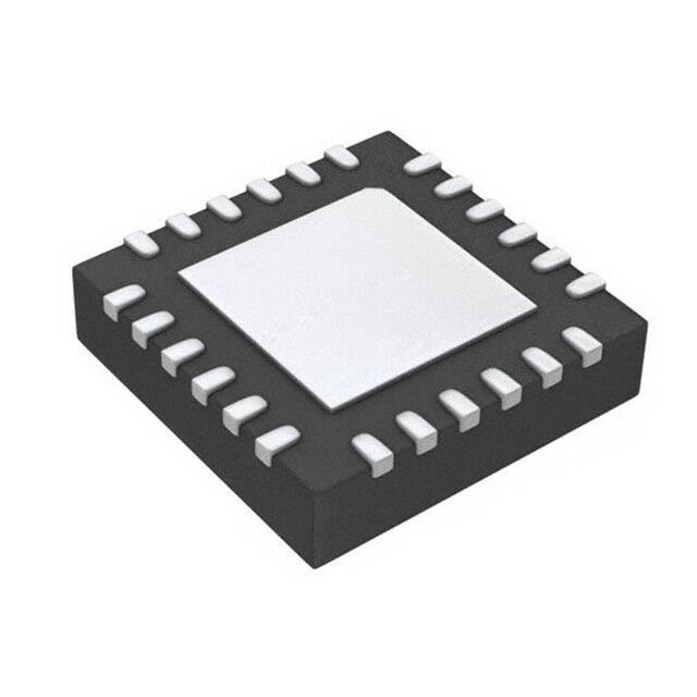


 工商网监
湘ICP备2023018690号
工商网监
湘ICP备2023018690号
