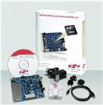
C8051T606-DK
C8051T606 D EVELOPMENT K IT U S E R ’ S G UIDE
es
ig
n
1. Kit Contents
The C8051T606 Development Kit contains the following items:
D
C8051T606 Main Board
C8051T606 MSOP Socket Daughter Board for programming MSOP devices
C8051T600 Emulation Daughter Board with C8051F300 installed
(5) C8051T606-GT Samples
C8051T606 Development Kit Quick-Start Guide
Silicon Laboratories IDE and Product Information CD-ROM. CD content includes the following:
Silicon
Laboratories Integrated Development Environment (IDE)
assembler, compiler and linker tools
Source code examples and register definition files
Documentation
Evaluation
AC to DC Universal Power Adapter
USB Cable
RS-232 Cable
fo
r
N
ew
Also available for purchase separately are socket daughter boards for the QFN-11 and QFN-10 packages.
m
en
de
d
2. About the Daughter Boards
om
The C8051T606 Development Kit includes two daughter boards: a C8051T600 Emulation Daughter Board and a
C8051T606 MSOP Socket Daughter Board. The emulation daughter board has a C8051F300 device installed,
which is a Flash-based device which can be used as a firmware development platform for the C8051T606. The
MSOP socket daughter board as well as the 10 and 11-pin QFN socket daughter boards (available separately) are
intended to allow programming of multiple C8051T606 devices and system-level debugging of these devices.
Once any byte location in aC8051T606 device has been programmed it cannot be erased, so it is advisable to use
the C8051F300 for the majority of code development. Refer to Application Note “AN280: Differences Between the
C8051F300 and the C8051T60x Device Family” for more details on how the C8051F300 can be used to develop
code for the C8051T606 and other members of the C8051T60x device family.
3. Hardware Setup
Refer to Figure 1 for a diagram of the hardware configuration.
ec
1. Attach the desired daughter board to the main board at connectors P1 and P2.
2. If using one of the socketed daughter boards, place the device to be programmed into the socket.
R
3. Connect the AC to DC power adapter to connector P3 on the main board.
4. Connect the main board to a PC running the Silicon Laboratories IDE using the USB cable.
N
ot
Notes:
Use the Reset icon in the IDE to reset the target when connected during a debug session.
Remove power from the main board and remove the USB cable before removing a daughter board from the
main board. Connecting or disconnecting a daughter board when the power adapter or USB cable are
connected can damage the main board, the daughter board, or the socketed device.
Likewise, remove power from the main board and remove the USB cable before removing a C8051T606 device
from the socket. Inserting or removing a device from the socket when the power adapter or USB cable are
connected can damage the main board, the daughter board, or the socketed device.
Rev. 0.1 3/09
Copyright © 2009 by Silicon Laboratories
C8051T606-DK
�C8051T606-DK
J9
D7
P3
J10
C8051T600 EDB
J8
AC Adapter
VPP
P1
C20
R18
R12
PWR
D4
F300
P2
USB Cable
N
ew
J1
es
ig
n
SILICON LABS
www.silabs.com
D
VDD
RESET
DEBUG
RX
TX
P0.3
P0.2
P0.5
P0.4
P0.3 SW
P0.2 LED
SW1
P0.2
D1
P0.3
fo
r
D2
J3
J2
Figure 1. Hardware Setup (Emulation Daughter Board Shown)
m
en
de
d
4. Software Setup
The included CD-ROM contains the Silicon Laboratories Integrated Development Environment (IDE), evaluation
8051 tools and additional documentation. Insert the CD-ROM into your PC’s CD-ROM drive. An installer will
automatically launch, allowing you to install the IDE software or read documentation by clicking buttons on the
Installation Panel. If the installer does not automatically start when you insert the CD-ROM, run autorun.exe found
in the root directory of the CD-ROM. Refer to the ReleaseNotes.txt file on the CD-ROM for the latest information
regarding the CD contents.
om
5. Silicon Laboratories Integrated Development Environment
ec
The Silicon Laboratories IDE integrates a source-code editor, source-level debugger and in-system programmer.
The use of third-party compilers, assemblers, and linkers is also supported. This development kit includes
evaluation versions of commercial ‘C’ compilers and assemblers which can be used from within the Silicon
Laboratories IDE.
5.1. System Requirements
Pentium-class host PC running Windows 2000 or later.
One available USB port.
N
ot
R
The Silicon Laboratories IDE requirements:
2
Rev. 0.1
�C8051T606-DK
5.2. Third-Party Toolsets
The Silicon Laboratories IDE has native support for many 8051 compilers. Natively-supported tools are as follows:
es
ig
n
Keil
IAR
Raisonance
Tasking
Hi-Tech
SDCC
Specific instructions for integrating each of the supported tools can be found in the application notes section of the
CD, or on the Silicon Labs web site (http://www.silabs.com).
D
5.3. Getting Started With the Silicon Labs IDE
N
ew
The following sections discuss how to create a new project with the IDE, build the source code, and download it to
the target device.
5.3.1. Creating a New Project
1. Select ProjectNew Project to open a new project and reset all configuration settings to default.
2. Select FileNew File to open an editor window. Create your source file(s) and save the file(s) with a recognized extension, such as .c, .h, or .asm, to enable color syntax highlighting.
fo
r
3. Right-click on “New Project” in the Project Window. Select Add files to project. Select files in the file
browser and click Open. Continue adding files until all project files have been added.
m
en
de
d
4. For each of the files in the Project Window that you want assembled, compiled and linked into the target
build, right-click on the file name and select Add file to build. Each file will be assembled or compiled as
appropriate (based on file extension) and linked into the build of the absolute object file.
Note: If a project contains a large number of files, the “Group” feature of the IDE can be used to organize.
Right-click on “New Project” in the Project Window. Select Add Groups to project. Add pre-defined
groups or add customized groups. Right-click on the group name and choose Add file to group. Select files
to be added. Continue adding files until all project files have been added.
5.3.2. Building and Downloading the Program for Debugging
1. Once all source files have been added to the target build, build the project by clicking on the Build/Make
Project button in the toolbar or selecting ProjectBuild/Make Project from the menu.
om
Note: After the project has been built the first time, the Build/Make Project command will only build the
files that have been changed since the previous build. To rebuild all files and project dependencies, click
on the Rebuild All button in the toolbar or select ProjectRebuild All from the menu.
R
ec
2. Before connecting to the target device, several connection options may need to be set. Open the
Connection Options window by selecting OptionsConnection Options... in the IDE menu. First, select
the “USB Debug Adapter” option. The USB Debug circuitry is integrated onto the C8051T606 main board.
Next, the correct “Debug Interface” must be selected. C8051T606 devices and the C8051F300 use Silicon
Labs “C2” 2-wire debug interface. Once all the selections are made, click the OK button to close the window.
N
ot
3. Click the Connect button in the toolbar or select DebugConnect from the menu to connect to the device.
4. Download the project to the target by clicking the Download Code button in the toolbar.
Note: To enable automatic downloading if the program build is successful select Enable automatic connect/download after build in the ProjectTarget Build Configuration dialog. If errors occur during the
build process, the IDE will not attempt the download.
Rev. 0.1
3
�C8051T606-DK
5. Save the project when finished with the debug session to preserve the current target build configuration,
editor settings and the location of all open debug views. To save the project, select ProjectSave Project
As... from the menu. Create a new name for the project and click on Save.
es
ig
n
6. Example Source Code
Example source code and register definition files are provided in the “SiLabs\MCU\Examples\C8051T60x”
directory during IDE installation. These files may be used as a template for code development. The comments in
each example file indicate which development tool chains were used when testing the.
6.1. Register Definition Files
D
Register definition files C8051T600.inc, C8051T600_defs.h and compiler_defs.h define all SFR registers and bitaddressable control/status bits. They are installed into the “SiLabs\MCU\Examples\C8051T60x” directory during
IDE installation. The register and bit names are identical to those used in the C8051T60x datasheet.
N
ew
7. Development Boards
fo
r
The C8051T606 Development Kit includes a main board which interfaces to various daughter boards. The
“C8051T600 Emulation Daughter Board” contains a C8051F300 device to be used for preliminary software
development. The socketed C8051T606 daughter boards allow programming and evaluation of the actual
C8051T606 devices. Numerous input/output (I/O) connections are provided on the main board to facilitate
prototyping. Refer to Figure 2 for the locations of the various connectors on the main board. Figure 3, Figure 4 and
Figure 5 show the available daughter boards that can be used with the C8051T606 main board.
P1, P2
Daughter board connection (Daughter boards are plugged into the P1 and P2 connectors for
evaluation and programming)
Power connector (accepts input from 7.5 to 15 VDC unregulated power adapter)
USB Debug connector
RS-232 connector
LED/Switch/RS-232 connection block
Direct device pin connection block
VPP supply connection (used when programming EPROM devices)
N
ot
R
ec
om
m
en
de
d
P3
J1
J2
J3
J8
J10
4
Rev. 0.1
�C8051T606-DK
J9
D7
VPP
P3
J10
P1
C20
R18
R12
D
J8
es
ig
n
SILICON LABS
www.silabs.com
VDD
RESET
PWR
N
ew
D4
J1
P2
DEBUG
D2
P0.5
P0.4
P0.3 SW
P0.2 LED
SW1
P0.2
D1
P0.3
m
en
de
d
RX
TX
P0.3
P0.2
fo
r
J3
J2
Figure 2. C8051T606 Main Board (Included in Kit)
F300
N
ot
R
ec
om
C8051T600 EDB
Figure 3. C8051T600 Evaluation Daughter Board (Included in Kit)
Rev. 0.1
5
�C8051T606-DK
U1
N
ew
D
PIN 1
es
ig
n
C8051T606 MSOP10 SKT DB
Figure 4. C8051T600 MSOP10 Socket Daughter Board (Included in Kit)
m
en
de
d
fo
r
C8051T600 QFN11 SKT DB
C8051T606 QFN10 SKT DB
N
ot
R
ec
om
Figure 5. C8051T600 3x3mm QFN11 Socket Daughter Board (Available Separately)
Figure 6. C8051T606 2x2mm QFN10 Socket Daughter Board (Available Separately)
6
Rev. 0.1
�C8051T606-DK
7.1. System Clock Sources
es
ig
n
The C8051T606 devices feature a calibrated internal oscillator which is enabled as the system clock source on
reset. After reset, the internal oscillator operates at a frequency of 24.5 MHz (±2%) by default, but may be
configured by software to operate at other frequencies. Therefore, in many applications an external oscillator is not
required. However, if you wish to operate the C8051T606 device at a frequency not available with the internal
oscillator, an external oscillator source may be used. Refer to the C8051T600/1/2/3/4/5/6 datasheet for more
information on configuring the system clock source.
D
The main board is designed to facilitate the use of external clock sources. To use an external CMOS clock source,
the clock can simply be applied to P0.3. To implement the RC mode option, placeholders for an 0805-packaged
capacitor (C20) and resistor (R18) are supplied on the board. The C (capacitor) clock option can be implemented
by using only the capacitor placeholder (C20). To reduce the amount of stray capacitance on the pin, which could
affect the frequency in either RC or C mode, resistor R12 can also be removed from the board when using C or RC
mode. Refer to the C8051T600/1/2/3/4/5/6 datasheet for more information on the use of external oscillators.
N
ew
7.2. Switches and LEDs
Two switches are provided on the main board. Switch RESET is connected to the RESET pin of the C8051T606.
Pressing RESET puts the device into its hardware-reset state. Switch P0.3 can be connected to the C8051T606’s
general purpose I/O (GPIO) pin P0.3 through header J3. Pressing Switch P0.3 generates a logic low signal on the
port pin. Remove the shorting block from the J3 header to disconnect Switch P0.3 from the port pin.
m
en
de
d
fo
r
Four LEDs are also provided on the target board. The red LED labeled PWR (D4) is used to indicate a power
connection to the target board. The red/green LED labeled D2 is the run/stop light for the debug circuitry. The red
LED labeled D7 indicates when the VPP programming voltage is being applied to the device (see Section 7.6 for
additional details). Finally, the green LED labeled P0.2 (D1) can be connected to the C8051T606’s GPIO pin P0.2
through header J3. Remove the shorting block from the header to disconnect the LED from the port pin. Note that
when this LED is connected, it will also light when programming EPROM devices.
See Table 1 for the port pins and headers corresponding to the switches, LEDs, and potentiometer.
Table 1. Target Board I/O Descriptions
I/O
Header
SW1
P0.3
J3[5–6]
SW2
RESET
none
Red LED
PWR
none
Green LED
P0.2
J3[7–8]
Red/Green LED
none
none
Red LED
VPP
J10
ec
om
Description
7.3. USB Debug Interface (DEBUG/J1)
N
ot
R
A Universal Serial Bus (USB) connector (J1) is included to provide the on-board debug and programming interface.
The debug/programming interface is powered through the USB connector, but requires power to the device via the
power connector P3 in order to initiate debug and programming operations.
Rev. 0.1
7
�C8051T606-DK
7.4. PORT I/O Connector (J8)
Each of the C8051T606’s I/O pins, as well as VPP, +3VD, GND, and /RST are routed to header J8. This header
can be used to easily connect to any signal on the device. Table 2 defines the pins for header J8.
Description
1
+3VD (+3.3 VDC)
2
VPP
3
no connection
4
P0.1
5
P0.2
6
P0.3
7
P0.4
8
P0.5
9
no connection
10
P0.7
11
GND
N
ew
fo
r
12
D
Pin #
es
ig
n
Table 2. J8 Pin Descriptions
/RST
m
en
de
d
7.5. Serial Interface (J2)
A RS232 transceiver circuit and DB-9 (J2) connector are provided on the main board to facilitate serial connections
to UART0 on the C8051T606. The TX and RX signals of UART0 may be connected to the RS-232 transceiver by
installing shorting blocks on header J3. The RTS and CTS lines do not have a direct connection available to the
C8051T606, due to limited pin resources on the device. However, these two signals have also been routed through
the transceiver, and are available for wiring on-board at test points near the DB-9 connector. The transceiver shifts
the UART signals to RS-232 levels, and connects to the appropriate pins on the DB-9 connector.
—Install shorting block to connect UART0 RX (P0.5) to transceiver.
—Install shorting block to connect UART0 TX (P0.4) to transceiver.
N
ot
R
ec
om
J3[1–2]
J3[3–4]
8
Rev. 0.1
�C8051T606-DK
7.6. VPP Connection (J10)
7.7. Using Alternate Supplies with the C8051T60x Development Kit
es
ig
n
The C8051T606 devices require a special 6.0 V programming voltage applied to the VPP pin during device
programming. The VPP pin on these devices is shared with P0.2. During programming, the VPP voltage is
automatically enabled when needed. Header J10 is provided to allow the user to disconnect the programming
circuitry from the VPP/P0.2 pin to avoid interfering with the normal application operation of P0.2. When
programming the device, J10 should be shorted with a shorting block. When running normal application code, J10
can be removed. Note that the C8051T600 emulation daughter board does not connect the main board’s VPP and
P0.2 signals, so removing the shorting block is not necessary when using the emulation daughter board.
N
ew
D
For most evaluation purposes, the on-board 3.3 V supply regulator is sufficient to be used as a VDD power supply.
However, in applications where a different supply voltage is desired (for example, 1.8 V), an external supply
voltage can be applied to the board at the analog connector (J6). Depending on the supply and the desired
functionality of the board, it may be necessary to cut the VDD supply voltage trace on the back of the board behind
header J9 (not populated). The following should be considered when supplying a different voltage to the device:
1. When programming a C8051T606 device: The on-board 3.3 V regulator should be used for VDD.
2. If a VDD supply voltage between 2.7 and 3.6 V is desired: The ac to dc power adapter should be
disconnected from P3, and the desired supply voltage can be applied directly to the GND and VDD terminals of
terminal block J6. No board modification is necessary.
fo
r
3. If a VDD supply voltage between 1.8 and 2.7 V is desired and RS-232 functionality is not required: The ac
to dc power adapter should be disconnected from P3, and the desired supply voltage can be applied directly to
the GND and VDD terminals of terminal block J6. No board modification is necessary.
N
ot
R
ec
om
m
en
de
d
4. If a VDD supply voltage between 1.8 and 2.7 V is desired and RS-232 functionality is required: The RS232 transceiver is not specified to operate below 2.7 V. In this case, the trace under header J9 should be cut.
Then, the desired VDD supply voltage can be applied directly to the GND and VDD terminals of terminal block
J6, and the ac to dc power adapter can be connected to P3, to provide 3.3 V to the RS-232 transceiver. In this
case, it may also be necessary to configure the TX pin on the device for open-drain mode, and add a pull-up
resistor to the supply of the transceiver.
Rev. 0.1
9
�N
ot
10
Rev. 0.1
m
en
de
d
fo
r
N
ew
Figure 7. C8051T600 Main Board Schematic (page 1/2)
om
ec
R
es
ig
n
D
C8051T606-DK
8. Schematics
�N
ot
Rev. 0.1
m
en
de
d
fo
r
N
ew
Figure 8. C8051T600 Main Board Schematic (page 2/2)
om
ec
R
es
ig
n
D
C8051T606-DK
11
�D
es
ig
n
C8051T606-DK
m
en
de
d
fo
r
N
ew
Figure 9. C8051T600 Emulation Daughter Board Schematic
ec
om
Figure 10. C8051T600 MSOP10 Socket Daughter Board Schematic
N
ot
R
Figure 11. C8051T600 QFN11 Socket Daughter Board Schematic
Figure 12. C8051T606 QFN10 Socket Daughter Board Schematic
12
Rev. 0.1
�es
ig
n
D
fo
r
N
ew
IoT Portfolio
www.silabs.com/IoT
om
One-click access to MCU and
wireless tools, documentation,
software, source code libraries &
more. Available for Windows,
Mac and Linux!
m
en
de
d
Simplicity Studio
SW/HW
Quality
Support and Community
www.silabs.com/simplicity
www.silabs.com/quality
community.silabs.com
N
ot
R
ec
Disclaimer
Silicon Laboratories intends to provide customers with the latest, accurate, and in-depth documentation of all peripherals and modules available for system and software implementers
using or intending to use the Silicon Laboratories products. Characterization data, available modules and peripherals, memory sizes and memory addresses refer to each specific
device, and "Typical" parameters provided can and do vary in different applications. Application examples described herein are for illustrative purposes only. Silicon Laboratories
reserves the right to make changes without further notice and limitation to product information, specifications, and descriptions herein, and does not give warranties as to the accuracy
or completeness of the included information. Silicon Laboratories shall have no liability for the consequences of use of the information supplied herein. This document does not imply
or express copyright licenses granted hereunder to design or fabricate any integrated circuits. The products must not be used within any Life Support System without the specific
written consent of Silicon Laboratories. A "Life Support System" is any product or system intended to support or sustain life and/or health, which, if it fails, can be reasonably expected
to result in significant personal injury or death. Silicon Laboratories products are generally not intended for military applications. Silicon Laboratories products shall under no
circumstances be used in weapons of mass destruction including (but not limited to) nuclear, biological or chemical weapons, or missiles capable of delivering such weapons.
Trademark Information
Silicon Laboratories Inc., Silicon Laboratories, Silicon Labs, SiLabs and the Silicon Labs logo, CMEMS®, EFM, EFM32, EFR, Energy Micro, Energy Micro logo and combinations
thereof, "the world’s most energy friendly microcontrollers", Ember®, EZLink®, EZMac®, EZRadio®, EZRadioPRO®, DSPLL®, ISOmodem ®, Precision32®, ProSLIC®, SiPHY®,
USBXpress® and others are trademarks or registered trademarks of Silicon Laboratories Inc. ARM, CORTEX, Cortex-M3 and THUMB are trademarks or registered trademarks of
ARM Holdings. Keil is a registered trademark of ARM Limited. All other products or brand names mentioned herein are trademarks of their respective holders.
Silicon Laboratories Inc.
400 West Cesar Chavez
Austin, TX 78701
USA
http://www.silabs.com
�


 工商网监
湘ICP备2023018690号
工商网监
湘ICP备2023018690号
