TouchXpress™ Family
CPT007B Data Sheet
The CPT007B device, part of the TouchXpress family, is designed
to quickly replace mechanical buttons with modern capacitive
touch buttons by eliminating firmware complexity and reducing development time.
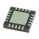
Supporting up to 7 capacitive sensor inputs in packages as small as a 3 mm x 3 mm
QFN, the CPT007B is a highly-integrated device that provides a simple solution for adding capacitive touch. The device also comes with advanced features like moisture immunity, wake-on proximity, and buzzer feedback for an enhanced user experience. No
firmware development is needed, and all the capacitive touch sense parameters can be
configured using a simple GUI-based configurator. By eliminating the need for complex
firmware development, the CPT007B device enables rapid user interface designs with
minimal development effort.
The CPT007B device is ideal for a wide range of capacitive touch applications, including
the following:
• Home appliances
• Instrument / Control panels
• White goods
Input
Features
KEY FEATURES
• No firmware development required
• Simple GUI-based configurator
• 7 Capacitive Sensor inputs with
programmable sensitivity
• 7 General purpose outputs (GPOs) to
communicate to the host processor or drive
LEDs
• Lowest power capacitive sense solution
• Active — 200 µA
• Sleep — 1 µA
• Wake on proximity
• Superior noise immunity: SNR up to 270:1
• Moisture immunity
• Mutually-exclusive touch qualifier
• Medical equipment
• Consumer electronics
• Lighting control
• Button touch time-out to avoid false
touches
• Buzzer output for audible touch feedback
Capacitive Touch Sensing
Features
Output
Features
Proximity Wake
Input
Touch
Qualification
MutuallyExclusive Touch
Qualifier
Configurable
Output Pin for
each Input
Input Engine
with
7 Inputs
Configuration
Profile for each
Input
Baselining
Optional Buzzer
Output
Low Power State
Machine
Touch Time-Out
Timer
Lowest power mode with feature operational:
Active
Optimized Active
Low Power Sleep
silabs.com | Smart. Connected. Energy-friendly.
This information applies to a product under development. Its characteristics and specifications are subject to change without notice.
Preliminary Rev. 0.2
�CPT007B Data Sheet
Feature List and Ordering Information
1. Feature List and Ordering Information
CP T 0 07 B – A 02 – G M R
Tape and Reel (Optional)
Package Type — QFN20 (M), QSOP24 (U)
Temperature Grade — –40 to +85 °C (G)
Firmware Revision
Hardware Revision
Capacitive Sense Features — Button (B)
Number of Capacitive Sense Inputs
Interface Type — GPO (0), I2C (1)
TouchXpress Family
Silicon Labs Xpress Product Line
Figure 1.1. CPT007B Part Numbering
The CPT007B has the following features:
• Capacitive sensing input engine with 7 inputs
• Post-sample touch qualification engine
• Configuration profile space in non-volatile memory
• Pin output with configurable polarity and drive strength
• Low power state machine to minimize current draw in all use cases
• Capacitive proximity sensing input
• Buzzer output
• Mutually exclusive touch qualifier
• Touch time-out timer
Package
QFN20
CPT007B-A02-GU
Yes
-40 to +85 °C
QSOP24
silabs.com | Smart. Connected. Energy-friendly.
(RoHS Compliant)
-40 to +85 °C
Pb-free
Yes
Part Number
CPT007B-A02-GM
Ordering
Temperature Range
Table 1.1. Product Selection Guide
Preliminary Rev. 0.2 | 1
�CPT007B Data Sheet
Typical Connection Diagrams
2. Typical Connection Diagrams
2.1 Signal, Analog, and Power Connections
Figure 2.1 Connection Diagram on page 2 shows a typical connection diagram for the power pins of CPT007B devices.
CPT007B
Device
1.8-3.6 V (in)
4.7 µF and 0.1 µF
bypass capacitors
required for the power
pins placed as close to
the pins as possible.
VDD
GND
Host
Processor
OUT00
OUT01
...
OUT06
CS00
Electrode
...
CS06
Electrode
1.8-3.6 V (in)
Config Data
Config Clk / RSTb
Figure 2.1. Connection Diagram
silabs.com | Smart. Connected. Energy-friendly.
Preliminary Rev. 0.2 | 2
�CPT007B Data Sheet
Typical Connection Diagrams
2.2 Configuration
The diagram below shows a typical connection diagram for the configuration connections pins. The ToolStick Base Adapter is available
on the evaluation board.
CPT007B Device
VDD
1k
Config Clk
Config Data
GND
ToolStick
Figure 2.2. Configuration Connection Diagram
silabs.com | Smart. Connected. Energy-friendly.
Preliminary Rev. 0.2 | 3
�CPT007B Data Sheet
Electrical Specifications
3. Electrical Specifications
3.1 Electrical Characteristics
All electrical parameters in all tables are specified under the conditions listed in Table 3.1 Recommended Operating Conditions on page
4, unless stated otherwise.
3.1.1 Recommended Operating Conditions
Table 3.1. Recommended Operating Conditions
Parameter
Symbol
Operating Supply Voltage on VDD
VDD
Minimum RAM Data Retention
Voltage on VDD1
VRAM
Operating Ambient Temperature
TA
Test Condition
Min
Typ
Max
Unit
1.8
2.4
3.6
V
Not in Sleep Mode
—
1.4
—
V
Sleep Mode
—
0.3
0.5
V
–40
—
85
°C
Note:
1. All voltages with respect to GND.
silabs.com | Smart. Connected. Energy-friendly.
Preliminary Rev. 0.2 | 4
�CPT007B Data Sheet
Electrical Specifications
3.1.2 Power Consumption
See 3.4 Typical Performance Curves for power consumption plots.
Table 3.2. Power Consumption
Parameter
Symbol
Active Mode Supply Current
Min
Typ
Max
Unit
IDD
—
3.1
—
mA
Optimized Active Mode Supply
Current
IDD
—
180
—
µA
Sleep Mode Current1, 2
IDD
3 sensors or fewer
—
0.78
—
µA
4 sensors
—
0.79
—
µA
5 sensors
—
0.81
—
µA
6 sensors
—
0.82
—
µA
7 sensors
—
0.84
—
µA
Scan period = 10 ms
—
154
—
µA
Scan period = 20 ms
—
77
—
µA
Scan period = 50 ms
—
31
—
µA
Scan period = 75 ms
—
21
—
µA
Scan period = 100 ms
—
16
—
µA
Scan period = 10 ms
—
47
—
µA
Scan period = 20 ms
—
23
—
µA
Scan period = 50 ms
—
9
—
µA
Scan period = 75 ms
—
6
—
µA
Scan period = 100 ms
—
5
—
µA
System Current with Varying Scan
Time — Base with One Sensor1
System Current with Varying Scan
Time — Each Additional Sensor1
IDD
IDD
Test Condition
Note:
1. Measured with Free Run Mode disabled and sensors set to 4x accumulation, 8x gain.
2. Measured with scan period set to 250 ms.
silabs.com | Smart. Connected. Energy-friendly.
Preliminary Rev. 0.2 | 5
�CPT007B Data Sheet
Electrical Specifications
3.1.3 Reset and Supply Monitor
Table 3.3. Reset and Supply Monitor
Parameter
Symbol
Test Condition
Min
Typ
Max
Unit
VDD Supply Monitor Threshold
VVDDM
Reset Trigger
1.7
1.75
1.8
V
VWARN
Early Warning
1.8
1.85
1.9
V
Power-On Reset (POR) Monitor
Threshold
VPOR
Rising Voltage on VDD
—
1.75
—
V
Falling Voltage on VDD
0.75
1.0
1.3
V
VDD Ramp Time
tRMP
—
—
3
ms
RST Low Time to Generate Reset
tRSTL
15
—
—
µs
Boot Time1
tboot
1 sensor
—
25
—
ms
2 sensors
—
40
—
ms
3 sensors
—
55
—
ms
4 sensors
—
70
—
ms
5 sensors
—
85
—
ms
6 sensors
—
100
—
ms
7 sensors
—
115
—
ms
Time to VDD ≥ 1.8 V
Note:
1. Boot time is defined as the time from a power-on reset or /RST pin release until the first capacitive sense scan begins.
3.1.4 Configuration Memory
Table 3.4. Configuration Memory
Parameter
Symbol
Endurance (Write/Erase Cycles)
NWE
Test Condition
Min
Typ
Max
Units
20 k
100 k
—
Cycles
Note:
1. Data Retention Information is published in the Quarterly Quality and Reliability Report.
silabs.com | Smart. Connected. Energy-friendly.
Preliminary Rev. 0.2 | 6
�CPT007B Data Sheet
Electrical Specifications
3.1.5 Capacitive Sense
Table 3.5. Capacitive Sense
Parameter
Symbol
Test Condition
Scan Time Per Sensor1
tSCAN
Signal to Noise Ratio1, 2
Conversion Time
Total Processing Time3
SNR
tCONV
tPROC
Maximum External Capacitive
Load
CEXTMAX
Maximum External Series Impedance
REXTMAX
silabs.com | Smart. Connected. Energy-friendly.
Min
Typ
Max
Unit
Accumulation = 1x
—
64
—
µs
Accumulation = 4x
—
256
—
µs
Accumulation = 8x
—
512
—
µs
Accumulation = 16x
—
1.024
—
ms
Accumulation = 32x
—
2.048
—
ms
Accumulation = 64x
—
4.096
—
ms
Accumulation = 1x
—
90:1
—
codes
Accumulation = 4x
—
180:1
—
codes
Accumulation = 8x
—
182:1
—
codes
Accumulation = 16x
—
210:1
—
codes
Accumulation = 32x
—
230:1
—
codes
Accumulation = 64x
—
270:1
—
codes
Gain = 1x
—
205
—
µs
Gain = 2x
—
123
—
µs
Gain = 3x
—
98
—
µs
Gain = 4x
—
85
—
µs
Gain = 5x
—
76
—
µs
Gain = 6x
—
72
—
µs
Gain = 7x
—
67
—
µs
Gain = 8x
—
64
—
µs
1 sensor
—
576
—
µs
2 sensors
—
796
—
µs
3 sensors
—
1.0
—
ms
4 sensors
—
1.2
—
ms
5 sensors
—
1.4
—
ms
6 sensors
—
1.7
—
ms
7 sensors
—
1.9
—
ms
Gain = 8x
—
45
—
pF
Gain = 1x
—
500
—
pF
Gain = 8x
—
50
—
kΩ
Preliminary Rev. 0.2 | 7
�CPT007B Data Sheet
Electrical Specifications
Parameter
Symbol
Test Condition
Min
Typ
Max
Unit
Note:
1. Measured with gain set to 8x.
2. Measured with an evaluation board with 1/16" overlay using Capacitive Sense Profiler.
3. Sensors configured to 8x gain, 1x accumulation with sensor sampling and system processing time included and mutually-exclusive buttons, buzzer, and touch time-outs disabled.
3.1.6 General Purpose and Buzzer Outputs
Table 3.6. General Purpose and Buzzer Outputs
Parameter
Symbol
Test Condition
Min
Typ
Max
Unit
Output High Voltage (High Drive)
VOH
IOH = –3 mA
VDD – 0.7
—
—
V
Output Low Voltage (High Drive)
VOL
IOL = 8.5 mA
—
—
0.6
V
Output High Voltage (Low Drive)
VOH
IOH = –1 mA
VDD – 0.7
—
—
V
Output Low Voltage (Low Drive)
VOL
IOL = 1.4 mA
—
—
0.6
V
Weak Pull-Up Current
IPU
VDD = 1.8 V
—
–4
—
µA
–35
–20
—
µA
Min
Typ
Max
Unit
VIN = 0 V
VDD = 3.6 V
VIN = 0 V
3.2 Thermal Conditions
Table 3.7. Thermal Conditions
Parameter
Symbol
Test Condition
Thermal Resistance*
θJA
QFN20 Packages
—
60
—
°C/W
QSOP24 Packages
—
65
—
°C/W
Note:
1. Thermal resistance assumes a multi-layer PCB with any exposed pad soldered to a PCB pad.
silabs.com | Smart. Connected. Energy-friendly.
Preliminary Rev. 0.2 | 8
�CPT007B Data Sheet
Electrical Specifications
3.3 Absolute Maximum Ratings
Stresses above those listed in Table 3.8 Absolute Maximum Ratings on page 9 may cause permanent damage to the device. This is
a stress rating only and functional operation of the devices at those or any other conditions above those indicated in the operation listings of this specification is not implied. Exposure to maximum rating conditions for extended periods may affect device reliability. For
more information on the available quality and reliability data, see the Quality and Reliability Monitor Report at http://www.silabs.com/
support/quality/pages/default.aspx.
Table 3.8. Absolute Maximum Ratings
Parameter
Symbol
Ambient Temperature Under Bias
Test Condition
Min
Max
Unit
TBIAS
–55
125
°C
Storage Temperature
TSTG
–65
150
°C
Voltage on VDD
VDD
GND–0.3
4.0
V
Voltage on I/O pins or RSTb
VIN
GND–0.3
VDD + 0.3
V
Total Current Sunk into Supply Pin
IVDD
—
400
mA
Total Current Sourced out of Ground
Pin
IGND
400
—
mA
Current Sourced or Sunk by Any I/O
Pin or RSTb
IIO
–100
100
mA
Maximum Total Current through all
Port Pins
IIOTOT
—
200
mA
Operating Junction Temperature
TJ
–40
105
°C
Exposure to maximum rating conditions for extended periods may affect device reliability.
silabs.com | Smart. Connected. Energy-friendly.
Preliminary Rev. 0.2 | 9
�CPT007B Data Sheet
Electrical Specifications
3.4 Typical Performance Curves
Figure 3.1. Active Mode Processing Time Per Sensor
Note: Active mode processing time per sensor measured with sensors configured to 1x accumulation, 8x gain. Sensor sampling and
system processing time is included with mutually-exclusive buttons, the buzzer, and touch time-outs disabled.
Figure 3.2. Current vs. Active Mode Scan Period — Base Current Consumption
silabs.com | Smart. Connected. Energy-friendly.
Preliminary Rev. 0.2 | 10
�CPT007B Data Sheet
Electrical Specifications
Figure 3.3. Current vs. Active Mode Scan Period — Current Consumption for Each Additional Sensor
Note: Active mode scan period current draw measured with free run mode disabled and all 7 sensors enabled at 4x accumulation, 8x
gain. In addition, the buzzer and mutually-exclusive button groups were disabled.
Figure 3.4. Typical VOH Curves
silabs.com | Smart. Connected. Energy-friendly.
Preliminary Rev. 0.2 | 11
�CPT007B Data Sheet
Electrical Specifications
Figure 3.5. Typical VOL Curves
silabs.com | Smart. Connected. Energy-friendly.
Preliminary Rev. 0.2 | 12
�CPT007B Data Sheet
Functional Description
4. Functional Description
4.1 Capacitive Sensing Input
4.1.1 Introduction
The capacitive to digital converter uses an iterative, charge-timing self-capacitance technique to measure capacitance on an input pin.
Sampling is configured and controlled by settings in the non-volatile configuration profile, which can be changed through the 2-pin configuration interface.
Capacitance
Active threshold
Inactive threshold
Touch delta
Baseline
Time
Figure 4.1. Capacitive Sense Data Types
4.1.2 Touch Qualification Criteria
The device detects a touch event when an inactive (untouched) input enabled by the input enable mask detects an sequence of measurements that cross the active threshold.
The device detects a touch release event when an active (touched) input enabled by the input enable mask detects an sequence of
measurements that cross the inactive threshold.
The debounce configuration profile parameter defines how many measurements in a row must cross a threshold before a touch or release is qualified. In electrically noisy environments more heavily filtered data is used for qualification.
4.1.3 Thresholds
Capacitive sensing inputs use input-specific thresholds for touch qualification. Each input uses two thresholds, one to detect inactive-toactive transitions on the input, and another to determine active-to-inactive transitions on the input. The inputs use two thresholds to add
hysteresis and prevent active/inactive ringing on inputs. Each threshold can be set through Simplicity Studio tools and all thresholds are
stored in non-volatile memory in the device's configuration profile.
Thresholds are defined as percentages of a capacitive sensing input's touch delta.
silabs.com | Smart. Connected. Energy-friendly.
Preliminary Rev. 0.2 | 13
�CPT007B Data Sheet
Functional Description
4.1.4 Debounce Counter
Each capacitive sensing input maintains its own debounce counter. For an inactive sensor, this counter tracks the number of successive samples which have crossed that input's active threshold. For an active sensor, this counter tracks the number of successive samples which have crossed the inactive threshold. When the counter reaches a terminal value defined in the the configuration profile, the
touch/release event is qualified.
4.1.5 Touch Deltas
Each capacitive sensing input uses a stored touch delta value that describes the expected difference between inactive and active capacitive sensing output codes. This value is stored in the configuration profile for the system and is used by the touch qualification engine, which defines inactive and active thresholds relative to the touch delta.
The touch deltas are stored in the configuration profile in a touch delta/16 format. For this reason, touch deltas must be configured as
multiples of 16.
4.1.6 Auto-Accumulation and Averaging
Capacitive sensing inputs have an auto-accumulate and average post-sample filter that can be used to improve signal strength if needed. Settings stored in the configuration profile can configure the engine to accumulate 1, 4, 8, 16, 32, or 64 samples. After the defined
number of samples have been accumulated, the result is divided by either 1, 4, 8, 16, 32, or 64, depending on the accumulation setting.
This auto-accumulated and averaged value is the sample output used for all touch qualification processing. Note that sample time per
sensor increases as the level of accumulation increases. To reduce current consumption, the engine should not be set to auto-accumulate unless it is required to achieve acceptable signal strength due to thick overlays or other system-level factors.
4.1.7 Drive strength
The drive strength of the current source used to charge the electrode being measured by the capacitive sensing input can be adjusted
in integer increments from 1x to 8x (8x is the default). High drive strength gives the best sensitivity and resolution for small capacitors,
such as those typically implemented as touch-sensitive PCB features. To measure larger capacitance values, the drive strength should
be lowered accordingly. The highest drive strength setting that yields capacitive sensing output which does not saturate the sensing
engine when the electrode is active (touched) should always be used to maximize input sensitivity.
4.1.8 Active Mode Scan Enable
Active mode scanning of capacitive sensing inputs is controlled by an enable setting for each capacitive sensing input. This setting is
stored in the configuration profile.
4.1.9 Active Mode Scan Period
The capacitive sensing input engine stays in active mode whenever one or more inputs have qualified as active. During this time, the
sensors scan at a periodicity defined by the active mode scan period, which is stored in the configuration profile. Every active mode
scan pushes new samples through the processing engine, which checks for new touch and release events on all enabled inputs.
If free run mode is enabled, the engine will repeatedly scan all enabled inputs during the active mode scan period. In this mode of
operation, the active mode scan period is used as a timer to determine how much time has passed since the last qualified active sensor
has been seen. When a defined amount of time without a qualified touch event has occurred, the engine switches to a low power mode
using the sleep mode scan period, and conserves current.
If free run mode is disabled, the engine will enter a low power state after completing one scan of all enabled inputs and processing the
resulting samples. The engine will remain in this low power state until it wakes, at a time defined by active mode scan period, to perform
another scan.
silabs.com | Smart. Connected. Energy-friendly.
Preliminary Rev. 0.2 | 14
�CPT007B Data Sheet
Functional Description
4.1.10 Active Mode Scan Type
The active mode scan type, which is stored in the configuration profile, controls whether the capacitive sensing engine in active mode
will scan only once during the active mode scan period before going to sleep, or whether the engine will continue scanning as quickly
as possible during the active mode scan period, never entering a low power state.
For optimal responsiveness, the engine should be configured to run with free run mode enabled. Setting the scan mode to 'free run'
causes touch qualification on a new touch to occur as quickly as the scanning engine can convert and process samples on all sensors.
In this mode, qualification time is not bounded by active mode scan period, and is only bounded by scanning configuration factors such
as the debounce setting, the number of enabled sensors, the accumulation setting on each sensor, and the timing constraints of any
enabled component.
For optimal current draw when in active mode, the engine should be configured to use the 'one scan per period' mode setting. In this
case, touch qualification is bound by the scan period and the debounce setting of the device.
Touch Event
(t = 0 ms)
Active
process
Optimized
Active
sample
10 ms
20 ms
additional
processing
30 ms
process
debounce
count = 1
additional
processing
sample
touch
qualified
sleep
Sleep
40 ms
sleep
Figure 4.2. Timing and Current — One Sample Per Period Mode
Touch Event
(t = 0 ms)
Active
process
Optimized
Active
sample
10 ms
additional
processing
20 ms
process
debounce
count = 1
30 ms
40 ms
additional
processing
sample
touch
qualified
Sleep
Figure 4.3. Timing and Current — Free Run Mode
4.1.11 Sleep Mode Scan Period
The sleep mode scan period defines the rate at which a scan of the inputs enabled as wake-up sources are sampled. Each enabled
sensor can also be enabled as a wake-up source. After the sleep mode scan completes, the scan is processed for a qualified candidate
touch. If a candidate touch is qualified, the system wakes form sleep mode and enters active mode scanning.
The sleep mode scan period is stored in the configuration profile and is defined in units of ms.
silabs.com | Smart. Connected. Energy-friendly.
Preliminary Rev. 0.2 | 15
�CPT007B Data Sheet
Functional Description
4.1.12 Active Mode and Sleep Mode Transitions
Capacitive sensing inputs will stay in active mode until no inputs detect qualified touches for a span of time defined by the counts until
sleep parameter stored in the configuration profile. The scan period of enabled inputs is defined by the active mode scan period, also
found in the configuration profile. If free run mode is enabled, the active mode sensing engine will remain awake and scanning the sensors as fast as possible. If free run mode is disabled, the engine will put itself into a low power state for the remainder of the active
mode scan period, after a scan has completed.
When in sleep mode, the sensing engine will wake at a period defined by sleep mode scan period to do a scan on sensors that have
been enabled as wakeup sources. If the engine finds a candidate touch in this state, the system reverts to active mode to continue
scanning.
Note that in systems where a proximity input is selected, the sleep mode scan engine uses conversions on the proximity input instead
of sensors enabled as wakeup sources.
Touch Delta
Devices configured to wake on a touch will attempt to qualify the candidate touch that initiated the sleep-to-active transition. If qualification completes successfully, the device will signal this qualification to the external system. Touch qualification of this candidate touch
uses the same active mode thresholds, debounce setting, and active mode scan period settings as any touch that occurs during active
mode scanning.
touch release
new touch
sleep scan sees
touch, wakes,
qualifies touch
qualified touch
release
no touch
counter = 0
no touch
counter = 1
Device Execution
t
no touch
counter = 2
...
no touch counter
= counts before
sleep
device enters
sleep
Figure 4.4. Active and Sleep Transitions
4.2 Pin Output
4.2.1 Introduction
Results of the capacitive sensing touch qualification engine are communicated through a set of digital output pins. The state of each pin
is bound to the touch qualification status of one capacitive sensing input pin. If a capacitive sensing input has qualified an active event,
the corresponding output pin will be set to its active state. If the input has qualified a release event is inactive, the corresponding output
pin will be set to its inactive state. Pin polarity and drive strength are configurable parameters.
silabs.com | Smart. Connected. Energy-friendly.
Preliminary Rev. 0.2 | 16
�CPT007B Data Sheet
Functional Description
4.2.2 Configuration
The configuration profile allows users to globally configure outputs as active high or active low. The configuration profile also allows
users to globally configure pins as open drain outputs or push-pull outputs.
4.3 Capacitive Proximity Sensing
4.3.1 Wake on Proximity
The wake on capacitive proximity detection engine monitors for the presence of a conductive object such as a hand to move within
detectable range of the sensor. When the engine detects an object, the device wakes from sleep and can begin qualifying touch events
on all sensors enabled for active mode sensing.
4.3.2 Proximity Sensing Output
Proximity sensing state is output using a designated Out pin on the CPT007B. By choosing this pin, the user is effectively disabling the
corresponding CS input pin. If the user is configuring proximity sensing to mode 2 operation, where a single capacitive sensing input pin
is used for proximity detection, it is recommended that this input pin be the pin that corresponds to the selected proximity Out pin.
4.3.3 Proximity Configuration
The proximity sensing feature uses a single sensor input for proximity qualification. The configuration profile stores the pin chosen by
the user. The sensor used for proximity qualification should also have a drive strength setting that is as high as possible without saturating the input when no conductive object is in proximity to the proximity sensor. The accumulation setting of the input is also configurable.
The proximity threshold controls the sensitivity of the input. A lower threshold setting increases sensitivity and increases the range of
the sensor.
A proximity sensing input cannot be used for touch qualification, and so the active and inactive thresholds are not used for proximity
sensors. Additionally, the proximity input has no effect on other components of the device such as mutually exclusive button groups,
buzzer output, touch time out timers, and sliders.
4.4 Touch Time-Out
The touch time-out feature can be enabled and disabled through the configuration profile. When enabled, the device will monitor touch
event duration on each input independently.
When a touch event exceeds a duration specified in the configuration profile, the device forces a release event, even if the user is still
actively touching the sensor.
The feature qualifies a touch release by adding the configured touch delta value for that sensor to the sensor's current baseline value.
By doing this, the raw data-to-baseline delta created by the touch will be removed, and the touch qualification engine will see this as a
touch release event.
When the user removes a finger from a sensor that had been qualified active but has been qualified released through touch timeout, the
resulting raw-to-baseline negative delta will be aggressively tracked downward by the baseline, resulting in a sensor that remains sensitive to successive touches.
The touch timeout duration is configured globally, so all inputs are monitored for the same touch duration.
If both the touch timeout feature and the mutually exclusive button group feature are enabled, the timeout timer will only run on the
touch that is externally reported as being active.
4.5 Buzzer Output
4.5.1 Introduction
The buzzer output engine produces a square wave of a configurable duration and frequency when a capacitive sensing input goes from
inactive to active. The feature can be enabled and disabled through the configuration profile. The configuration profile also includes the
settings for active duration and frequency.
silabs.com | Smart. Connected. Energy-friendly.
Preliminary Rev. 0.2 | 17
�CPT007B Data Sheet
Functional Description
Device Execution
Active
process
Optimized
Active
sample
additional
processing
process
additional
processing
sample
sleep
Sleep
sleep
No Touch, Buzzer Inactive
Figure 4.5. Effects of the Buzzer on Current Draw — Active Mode, No Touch, Buzzer Inactive
Device Execution
process
Active
sample
additional
processing
sleep
(stall)
process
sample
additional
processing
sleep
(stall)
Optimized
Active
Sleep
Touch Detected, Buzzer Active
Figure 4.6. Effects of the Buzzer on Current Draw — Active Mode, Touch Detected, Buzzer Active
4.5.2 Buzzer Configuration
If enabled, buzzer output will be routed to the Buzzer pin (pin 7) of the CPT007B. When activated, the buzzer will remain active for
either the duration specified in the configuration profile, or until the last active sensor has qualified a touch release.
The configuration profile supports configuration of output frequencies ranging from 1 kHz to 4 kHz.
The configuration profile can configure the buzzer output pin to either push pull mode or open drain mode.
4.6 Mutually Exclusive Buttons
When enabled through the configuration profile, this system allows one and only one capacitive sensing input to be qualified as active
at a time. The first sensor active will remain the only sensor active until released. The device will internally qualify multiple touch and
release events but will not report them.
silabs.com | Smart. Connected. Energy-friendly.
Preliminary Rev. 0.2 | 18
�CPT007B Data Sheet
Functional Description
If multiple sensors have been internally qualified as active, the first sensor's touch event will be reported. If a touch event occurs simultaneously on more than one sensor, the touch with the highest touch delta will be reported.
If two sensors are qualified as active and the sensor being reported as active qualifies a touch release, the device will report that release and then report a touch qualification on the still-active second sensor.
In the case where a device has simultaneously qualified more than two active sensors and the reported active sensor qualifies and
reports a release, the remaining qualified sensor with the highest sensor name will then be reported. For example, if sensors CS00,
CS01, and CS02 are active with CS00 externally reported as active, after CS00's release, CS02 would be externally reported as an
active sensor unless the device has already qualified a touch release on CS02.
If both the touch timeout feature and the mutually exclusive button group feature are enabled, the timeout timer will only run on the
touch that is externally reported as being active.
CS00
CS01
CS02
Device Execution
physical touch on pad
touch reported by CPT device
release reported by CPT device
Figure 4.7. Mutually-Exclusive Button Operation
4.7 Self Testing
4.7.1 Introduction
When the self-test feature is enabled through the configuration profile, the device performs a check on all enabled capacitive sensing
inputs upon startup to determine whether the sensing input pins are erroneously shorted to ground or supply. If a short or open is found
on a sensor, the self test feature will signal that an error has been found through a port pin. The feature will then disable that sensor
before beginning touch qualification scans on all sensors left enabled.
4.7.2 Test Failure Signaling
If the self test check reveals an error, the device will toggle the buzzer output pin at a frequency of 2 Hz. This toggling will persist for two
seconds if the device detects one or more self test errors.
silabs.com | Smart. Connected. Energy-friendly.
Preliminary Rev. 0.2 | 19
�CPT007B Data Sheet
Functional Description
4.8 Configuration Profile
The configuration interface is used by the device to configure default values and performance characteristics that effect capacitive
sensing. The configuration data can be programmed through the Configuration interface (Config Clk and Config Data pins) using [Configurator] in Simplicity Studio.
Several configuration profile templates are available in Simplicity Studio to provide a starting point for development.
silabs.com | Smart. Connected. Energy-friendly.
Preliminary Rev. 0.2 | 20
�CPT007B Data Sheet
Pin Definitions
5. Pin Definitions
RSTb /
Config Clk
5
Config Data
6
CS02
CS03
CS04
CS05
19
18
17
(Top View)
GND
10
4
16
CS06
15
OUT00
14
OUT01
13
OUT02
12
GND
11
OUT03
OUT04
VDD
20 pin QFN
9
3
OUT05
GND
8
2
OUT06
CS00
7
1
BUZZER
CS01
20
5.1 CPT007B QFN20 Pin Definitions
Figure 5.1. CPT007B QFN20 Pinout
Table 5.1. Pin Definitions for CPT007B QFN20
Pin
Pin Name
Description
CS01
Analog input
Number
1
Capactive sensing input 1
2
CS00
Analog input
Capacitive sensing input 0
3
GND
Ground
4
VDD
Supply power input
5
RSTb /
Active-low reset /
Config Clk
Configuration clock
Config Data
Configuration data
6
silabs.com | Smart. Connected. Energy-friendly.
Preliminary Rev. 0.2 | 21
�CPT007B Data Sheet
Pin Definitions
Pin
Pin Name
Description
Buzzer
Push-pull output
Number
7
Buzzer output
8
OUT06
Push-pull output
Sensing state of CS06
9
OUT05
Push-pull output
Sensing state of CS05
10
OUT04
Push-pull output
Sensing state of CS04
11
OUT03
Push-pull output
Sensing state of CS03
12
GND
Ground
13
OUT02
Push-pull output
Sensing state of CS02
14
OUT01
Push-pull output
Sensing state of CS01
15
OUT00
Push-pull output
Sensing state of CS00
16
CS06
Analog input
Capacitive sensing input 6
17
CS05
Analog input
Capacitive sensing input 5
18
CS04
Analog input
Capacitive sensing input 4
19
CS03
Analog input
Capacitive sensing input 3
20
CS02
Analog input
Capacitive sensing input 2
silabs.com | Smart. Connected. Energy-friendly.
Preliminary Rev. 0.2 | 22
�CPT007B Data Sheet
Pin Definitions
5.2 CPT007B QSOP24 Pin Definitions
CS02
1
24
CS03
CS01
2
23
CS04
CS00
3
22
CS05
N/C
4
21
CS06
GND
5
20
OUT00
VDD
6
19
OUT01
N/C
7
18
OUT02
N/C
8
17
OUT03
RSTb /
Config Clk
9
16
OUT04
Config Data
10
15
N/C
BUZZER
11
14
OUT05
OUT06
12
13
N/C
24 pin QSOP
(Top View)
Figure 5.2. CPT007B QSOP24 Pinout
Table 5.2. Pin Definitions for CPT007B QSOP24
Pin
Pin Name
Description
CS02
Analog input
Number
1
Capacitive sensing input 2
2
CS01
Analog input
Capactive sensing input 1
3
CS00
Analog input
Capacitive sensing input 0
4
N/C
No Connect (leave this pin floating)
5
GND
Ground
silabs.com | Smart. Connected. Energy-friendly.
Preliminary Rev. 0.2 | 23
�CPT007B Data Sheet
Pin Definitions
Pin
Pin Name
Description
6
VDD
Supply power input
7
N/C
No Connect (leave this pin floating)
8
N/C
No Connect (leave this pin floating)
9
RSTb /
Active-low reset /
Config Clk
Configuration clock
10
Config Data
Configuration data
11
Buzzer
Push-pull output
Number
Buzzer output
12
OUT06
Push-pull output
Sensing state of CS06
13
N/C
No Connect (leave this pin floating)
14
OUT05
Push-pull output
Sensing state of CS05
15
N/C
No Connect (leave this pin floating)
16
OUT04
Push-pull output
Sensing state of CS04
17
OUT03
Push-pull output
Sensing state of CS03
18
OUT02
Push-pull output
Sensing state of CS02
19
OUT01
Push-pull output
Sensing state of CS01
20
OUT00
Push-pull output
Sensing state of CS00
21
CS06
Analog input
Capacitive sensing input 6
22
CS05
Analog input
Capacitive sensing input 5
23
CS04
Analog input
Capacitive sensing input 4
24
CS03
Analog input
Capacitive sensing input 3
silabs.com | Smart. Connected. Energy-friendly.
Preliminary Rev. 0.2 | 24
�CPT007B Data Sheet
QFN20 Package Specifications
6. QFN20 Package Specifications
6.1 QFN20 Package Dimensions
Figure 6.1. QFN20 Package Drawing
Table 6.1. QFN20 Package Dimensions
Dimension
Min
Typ
Max
A
0.50
0.55
0.60
A1
0.00
—
0.05
b
0.20
0.25
0.30
b1
0.275
0.325
0.375
D
D2
3.00 BSC
1.6
1.70
e
0.50 BSC
e1
0.513 BSC
E
3.00 BSC
1.80
E2
1.60
1.70
1.80
L
0.35
0.40
0.45
silabs.com | Smart. Connected. Energy-friendly.
Preliminary Rev. 0.2 | 25
�CPT007B Data Sheet
QFN20 Package Specifications
Dimension
Min
Typ
Max
L1
0.00
—
0.10
aaa
—
0.10
—
bbb
—
0.10
—
ddd
—
0.05
—
eee
—
—
0.08
Note:
1. All dimensions shown are in millimeters (mm) unless otherwise noted.
2. Dimensioning and Tolerancing per ANSI Y14.5M-1994.
3. This drawing is based upon JEDEC Solid State Product Outline MO-248 but includes custom features which are toleranced per
supplier designation.
4. Recommended card reflow profile is per the JEDEC/IPC J-STD-020 specification for Small Body Components.
silabs.com | Smart. Connected. Energy-friendly.
Preliminary Rev. 0.2 | 26
�CPT007B Data Sheet
QFN20 Package Specifications
6.2 QFN20 PCB Land Pattern
Figure 6.2. QFN20 PCB Land Pattern Drawing
Table 6.2. QFN20 PCB Land Pattern Dimensions
Dimension
Min
Max
C1
2.70
C2
2.70
C3
2.53
C4
2.53
E
0.50 REF
X1
0.20
0.30
X2
0.24
.034
X3
1.70
1.80
Y1
0.50
0.60
Y2
0.24
0.34
Y3
1.70
1.80
silabs.com | Smart. Connected. Energy-friendly.
Preliminary Rev. 0.2 | 27
�CPT007B Data Sheet
QFN20 Package Specifications
Dimension
Min
Max
Note:
1. All dimensions shown are in millimeters (mm) unless otherwise noted.
2. Dimensioning and Tolerancing is per the ANSI Y14.5M-1994 specification.
3. This Land Pattern Design is based on the IPC-7351 guidelines.
4. All metal pads are to be non-solder mask defined (NSMD). Clearance between the solder mask and the metal pad is to be 60 µm
minimum, all the way around the pad.
5. A stainless steel, laser-cut and electro-polished stencil with trapezoidal walls should be used to assure good solder paste release.
6. The stencil thickness should be 0.125 mm (5 mils).
7. The ratio of stencil aperture to land pad size should be 1:1 for the perimeter pads.
8. A 2x2 array of 0.75 mm openings on a 0.95 mm pitch should be used for the center pad to assure proper paste volume.
9. A No-Clean, Type-3 solder paste is recommended.
10. The recommended card reflow profile is per the JEDEC/IPC J-STD-020 specification for Small Body Components.
6.3 QFN20 Package Marking
007B
TTTT
YWW+
Figure 6.3. QFN20 Package Marking
The package marking consists of:
• 007B – The part number designation.
• TTTT – A trace or manufacturing code. The first letter of this code is the hardware revision.
• Y – The last digit of the assembly year.
• WW – The 2-digit workweek when the device was assembled.
• + – Indicates the device is RoHS-compliant.
silabs.com | Smart. Connected. Energy-friendly.
Preliminary Rev. 0.2 | 28
�CPT007B Data Sheet
QSOP24 Package Specifications
7. QSOP24 Package Specifications
7.1 QSOP24 Package Dimensions
Figure 7.1. QSOP24 Package Drawing
Table 7.1. QSOP24 Package Dimensions
Dimension
Min
Typ
Max
A
—
—
1.75
A1
0.10
—
0.25
b
0.20
—
0.30
c
0.10
—
0.25
D
8.65 BSC
E
6.00 BSC
E1
3.90 BSC
e
0.635 BSC
L
theta
silabs.com | Smart. Connected. Energy-friendly.
0.40
—
1.27
0º
—
8º
Preliminary Rev. 0.2 | 29
�CPT007B Data Sheet
QSOP24 Package Specifications
Dimension
Min
Typ
aaa
0.20
bbb
0.18
ccc
0.10
ddd
0.10
Max
Note:
1. All dimensions shown are in millimeters (mm) unless otherwise noted.
2. Dimensioning and Tolerancing per ANSI Y14.5M-1994.
3. This drawing conforms to JEDEC outline MO-137, variation AE.
4. Recommended card reflow profile is per the JEDEC/IPC J-STD-020 specification for Small Body Components.
silabs.com | Smart. Connected. Energy-friendly.
Preliminary Rev. 0.2 | 30
�CPT007B Data Sheet
QSOP24 Package Specifications
7.2 QSOP24 PCB Land Pattern
Figure 7.2. QSOP24 PCB Land Pattern Drawing
Table 7.2. QSOP24 PCB Land Pattern Dimensions
Dimension
Min
Max
C
5.20
5.30
E
0.635 BSC
X
0.30
0.40
Y
1.50
1.60
Note:
1. All dimensions shown are in millimeters (mm) unless otherwise noted.
2. This land pattern design is based on the IPC-7351 guidelines.
3. All metal pads are to be non-solder mask defined (NSMD). Clearance between the solder mask and the metal pad is to be 60 µm
minimum, all the way around the pad.
4. A stainless steel, laser-cut and electro-polished stencil with trapezoidal walls should be used to assure good solder paste release.
5. The stencil thickness should be 0.125 mm (5 mils).
6. The ratio of stencil aperture to land pad size should be 1:1 for all perimeter pads.
7. A No-Clean, Type-3 solder paste is recommended.
8. The recommended card reflow profile is per the JEDEC/IPC J-STD-020 specification for Small Body Components.
silabs.com | Smart. Connected. Energy-friendly.
Preliminary Rev. 0.2 | 31
�CPT007B Data Sheet
QSOP24 Package Specifications
7.3 QSOP24 Package Marking
e3
CPT007B
YYWWTTTTTT
Figure 7.3. QSOP24 Package Marking
The package marking consists of:
• CPT007B – The part number designation.
• TTTTTT – A trace or manufacturing code. The first letter of this code is the hardware revision.
• YY – The last two digits of the assembly year.
• WW – The 2-digit workweek when the device was assembled.
• e3 – Indicates the device is RoHS-compliant.
silabs.com | Smart. Connected. Energy-friendly.
Preliminary Rev. 0.2 | 32
�CPT007B Data Sheet
Relevant Application Notes
8. Relevant Application Notes
The following Application Notes are applicable to the CPT007B devices:
• AN957: TouchXpress™ Configuration and Profiling Guide — This application note guides developers through the evaluation and
configuration process of TouchXpress devices using Simplicity Studio [Xpress Configurator] and [Capacitive Sense Profiler].
• AN447: Printed Circuit Design Notes for Capacitive Sensing Performance — This document describes hardware design guidelines
specifically for capacitive sensing applications, including button placement and other layout guidelines.
• AN949: TouchXpress™ Programming Guide — This application note discusses the production programming options available for
TouchXpress devices.
Application Notes can be accessed on the Silicon Labs website (www.silabs.com/interface-appnotes) or in Simplicity Studio using the
[Application Notes] tile.
silabs.com | Smart. Connected. Energy-friendly.
Preliminary Rev. 0.2 | 33
�CPT007B Data Sheet
Revision History
9. Revision History
9.1 Revision 0.2
August 12th, 2016
Added new revision devices (A02).
Added QSOP24 devices, including pinout information and package drawings.
Added a paragraph to 4.1.12 Active Mode and Sleep Mode Transitions describing the wake-on-touch behavior.
9.2 Revision 0.1
November 21st, 2015
Initial release.
silabs.com | Smart. Connected. Energy-friendly.
Preliminary Rev. 0.2 | 34
�Table of Contents
1. Feature List and Ordering Information . . . . . . . . . . . . . . . . . . . . . . 1
2. Typical Connection Diagrams . . . . . . . . . . . . . . . . . . . . . . . . . 2
2.1 Signal, Analog, and Power Connections .
.
.
.
.
.
.
.
.
.
.
.
.
.
.
.
.
.
.
.
. 2
2.2 Configuration .
.
.
.
.
.
.
.
.
.
.
.
.
.
.
.
.
.
.
.
. 3
.
.
.
.
.
.
.
.
.
3. Electrical Specifications . . . . . . . . . . . . . . . . . . . . . . . . . . . 4
3.1 Electrical Characteristics . . . . .
3.1.1 Recommended Operating Conditions
3.1.2 Power Consumption . . . . . .
3.1.3 Reset and Supply Monitor . . . .
3.1.4 Configuration Memory . . . . .
3.1.5 Capacitive Sense . . . . . . .
3.1.6 General Purpose and Buzzer Outputs
.
.
.
.
.
.
.
.
.
.
.
.
.
.
.
.
.
.
.
.
.
.
.
.
.
.
.
.
.
.
.
.
.
.
.
.
.
.
.
.
.
.
.
.
.
.
.
.
.
.
.
.
.
.
.
.
.
.
.
.
.
.
.
.
.
.
.
.
.
.
.
.
.
.
.
.
.
.
.
.
.
.
.
.
.
.
.
.
.
.
.
.
.
.
.
.
.
.
.
.
.
.
.
.
.
.
.
.
.
.
.
.
.
.
.
.
.
.
.
.
.
.
.
.
.
.
.
.
.
.
.
.
.
.
.
.
.
.
.
.
.
.
.
.
.
.
.
3.2 Thermal Conditions .
.
.
4
4
5
6
6
7
8
.
.
.
.
.
.
.
.
.
.
.
.
.
.
.
.
.
.
.
.
.
.
.
.
. 8
3.3 Absolute Maximum Ratings .
.
.
.
.
.
.
.
.
.
.
.
.
.
.
.
.
.
.
.
.
.
.
.
. 9
3.4 Typical Performance Curves .
.
.
.
.
.
.
.
.
.
.
.
.
.
.
.
.
.
.
.
.
.
.
.
.10
4. Functional Description. . . . . . . . . . . . . . . . . . . . . . . . . . .
13
4.1 Capacitive Sensing Input . . . . . . .
4.1.1 Introduction . . . . . . . . . . .
4.1.2 Touch Qualification Criteria . . . . . .
4.1.3 Thresholds . . . . . . . . . . .
4.1.4 Debounce Counter . . . . . . . .
4.1.5 Touch Deltas . . . . . . . . . .
4.1.6 Auto-Accumulation and Averaging . . .
4.1.7 Drive strength . . . . . . . . . .
4.1.8 Active Mode Scan Enable . . . . . .
4.1.9 Active Mode Scan Period . . . . . .
4.1.10 Active Mode Scan Type . . . . . .
4.1.11 Sleep Mode Scan Period . . . . . .
4.1.12 Active Mode and Sleep Mode Transitions
.
.
.
.
.
.
.
.
.
.
.
.
.
.
.
.
.
.
.
.
.
.
.
.
.
.
.
.
.
.
.
.
.
.
.
.
.
.
.
.
.
.
.
.
.
.
.
.
.
.
.
.
.
.
.
.
.
.
.
.
.
.
.
.
.
.
.
.
.
.
.
.
.
.
.
.
.
.
.
.
.
.
.
.
.
.
.
.
.
.
.
.
.
.
.
.
.
.
.
.
.
.
.
.
.
.
.
.
.
.
.
.
.
.
.
.
.
.
.
.
.
.
.
.
.
.
.
.
.
.
.
.
.
.
.
.
.
.
.
.
.
.
.
.
.
.
.
.
.
.
.
.
.
.
.
.
.
.
.
.
.
.
.
.
.
.
.
.
.
.
.
.
.
.
.
.
.
.
.
.
.
.
.
.
.
.
.
.
.
.
.
.
.
.
.
.
.
.
.
.
.
.
.
.
.
.
.
.
.
.
.
.
.
.
.
.
.
.
.
.
.
.
.
.
.
.
.
.
.
.
.
.
.
.
.13
.13
.13
.13
.14
.14
.14
.14
.14
.14
.15
.15
.16
4.2 Pin Output . .
4.2.1 Introduction .
4.2.2 Configuration
.
.
.
.
.
.
.
.
.
.
.
.
.
.
.
.
.
.
.
.
.
.
.
.
.
.
.
.
.
.
.
.
.
.
.
.
.
.
.
.
.
.
.
.
.
.
.
.
.
.
.
.
.
.
.
.
.
.
.
.
.
.
.
.
.
.
.
.
.
.
.
.
.
.
.
.
.
.
.16
.16
.17
4.3 Capacitive Proximity Sensing.
4.3.1 Wake on Proximity . . .
4.3.2 Proximity Sensing Output .
4.3.3 Proximity Configuration . .
.
.
.
.
.
.
.
.
.
.
.
.
.
.
.
.
.
.
.
.
.
.
.
.
.
.
.
.
.
.
.
.
.
.
.
.
.
.
.
.
.
.
.
.
.
.
.
.
.
.
.
.
.
.
.
.
.
.
.
.
.
.
.
.
.
.
.
.
.
.
.
.
.
.
.
.
.
.
.
.
.
.
.
.
.
.
.
.
.
.
.
.
.17
.17
.17
.17
4.4 Touch Time-Out .
.
.
.
.
.
.
.
.
.
.
.
.
.
.
.
.
.
.
.
.
.
.
.
.
.
.
.
.
.
.
.
.
.
.17
4.5 Buzzer Output . . . .
4.5.1 Introduction . . . .
4.5.2 Buzzer Configuration .
.
.
.
.
.
.
.
.
.
.
.
.
.
.
.
.
.
.
.
.
.
.
.
.
.
.
.
.
.
.
.
.
.
.
.
.
.
.
.
.
.
.
.
.
.
.
.
.
.
.
.
.
.
.
.
.
.
.
.
.
.
.
.
.
.
.
.
.
.
.
.
.
.
.
.
.17
.17
.18
4.6 Mutually Exclusive Buttons
.
.
.
.
.
.
.
.
.
.
.
.
.
.
.
.
.
.
.
.
.
.
.
.
.18
Table of Contents
35
�4.7 Self Testing . . . .
4.7.1 Introduction . . . .
4.7.2 Test Failure Signaling
.
.
.
.
.
.
.
.
.
.
.
.
.
.
.
.
.
.
.
.
.
.
.
.
.
.
.
.
.
.
.
.
.
.
.
.
.
.
.
.
.
.
.
.
.
.
.
.
.
.
.
.
.
.
.
.
.
.
.
.
.
.
.
.
.
.
.
.
.
.
.
.
.
.
.
.19
.19
.19
4.8 Configuration Profile.
.
.
.
.
.
.
.
.
.
.
.
.
.
.
.
.
.
.
.
.
.
.
.
.
.
.20
5. Pin Definitions . . . . . . . . . . . . . . . . . . . . . . . . . . . . . .
21
.
5.1 CPT007B QFN20 Pin Definitions
.
.
.
.
.
.
.
.
.
.
.
.
.
.
.
.
.
.
.
.
.
.
.21
5.2 CPT007B QSOP24 Pin Definitions .
.
.
.
.
.
.
.
.
.
.
.
.
.
.
.
.
.
.
.
.
.
.23
6. QFN20 Package Specifications. . . . . . . . . . . . . . . . . . . . . . . .
25
6.1 QFN20 Package Dimensions
.
.
.
.
.
.
.
.
.
.
.
.
.
.
.
.
.
.
.
.
.
.
.
.25
6.2 QFN20 PCB Land Pattern
.
.
.
.
.
.
.
.
.
.
.
.
.
.
.
.
.
.
.
.
.
.
.
.
.27
6.3 QFN20 Package Marking .
.
.
.
.
.
.
.
.
.
.
.
.
.
.
.
.
.
.
.
.
.
.
.
.
.28
7. QSOP24 Package Specifications . . . . . . . . . . . . . . . . . . . . . . .
29
7.1 QSOP24 Package Dimensions .
.
.
.
.
.
.
.
.
.
.
.
.
.
.
.
.
.
.
.
.
.
.
.29
7.2 QSOP24 PCB Land Pattern .
.
.
.
.
.
.
.
.
.
.
.
.
.
.
.
.
.
.
.
.
.
.
.
.31
7.3 QSOP24 Package Marking .
.
.
.
.
.
.
.
.
.
.
.
.
.
.
.
.
.
.
.
.
.
.
.
.32
8. Relevant Application Notes . . . . . . . . . . . . . . . . . . . . . . . . .
33
9. Revision History . . . . . . . . . . . . . . . . . . . . . . . . . . . . .
34
9.1 Revision 0.2
.
.
.
.
.
.
.
.
.
.
.
.
.
.
.
.
.
.
.
.
.
.
.
.
.
.
.
.
.
.34
9.2 Revision 0.1
.
.
.
.
.
.
.
.
.
.
.
.
.
.
.
.
.
.
.
.
.
.
.
.
.
.
.
.
.
.34
Table of Contents . . . . . . . . . . . . . . . . . . . . . . . . . . . . . .
35
Table of Contents
36
�Simplicity Studio
One-click access to MCU and
wireless tools, documentation,
software, source code libraries &
more. Available for Windows,
Mac and Linux!
IoT Portfolio
www.silabs.com/IoT
SW/HW
www.silabs.com/simplicity
Quality
www.silabs.com/quality
Support and Community
community.silabs.com
Disclaimer
Silicon Laboratories intends to provide customers with the latest, accurate, and in-depth documentation of all peripherals and modules available for system and software implementers using
or intending to use the Silicon Laboratories products. Characterization data, available modules and peripherals, memory sizes and memory addresses refer to each specific device, and
"Typical" parameters provided can and do vary in different applications. Application examples described herein are for illustrative purposes only. Silicon Laboratories reserves the right to
make changes without further notice and limitation to product information, specifications, and descriptions herein, and does not give warranties as to the accuracy or completeness of the
included information. Silicon Laboratories shall have no liability for the consequences of use of the information supplied herein. This document does not imply or express copyright licenses
granted hereunder to design or fabricate any integrated circuits. The products are not designed or authorized to be used within any Life Support System without the specific written consent
of Silicon Laboratories. A "Life Support System" is any product or system intended to support or sustain life and/or health, which, if it fails, can be reasonably expected to result in significant
personal injury or death. Silicon Laboratories products are not designed or authorized for military applications. Silicon Laboratories products shall under no circumstances be used in
weapons of mass destruction including (but not limited to) nuclear, biological or chemical weapons, or missiles capable of delivering such weapons.
Trademark Information
Silicon Laboratories Inc.® , Silicon Laboratories®, Silicon Labs®, SiLabs® and the Silicon Labs logo®, Bluegiga®, Bluegiga Logo®, Clockbuilder®, CMEMS®, DSPLL®, EFM®, EFM32®,
EFR, Ember®, Energy Micro, Energy Micro logo and combinations thereof, "the world’s most energy friendly microcontrollers", Ember®, EZLink®, EZRadio®, EZRadioPRO®, Gecko®,
ISOmodem®, Precision32®, ProSLIC®, Simplicity Studio®, SiPHY®, Telegesis, the Telegesis Logo®, USBXpress® and others are trademarks or registered trademarks of Silicon Laboratories Inc. ARM, CORTEX, Cortex-M3 and THUMB are trademarks or registered trademarks of ARM Holdings. Keil is a registered trademark of ARM Limited. All other products or brand
names mentioned herein are trademarks of their respective holders.
Silicon Laboratories Inc.
400 West Cesar Chavez
Austin, TX 78701
USA
http://www.silabs.com
�


 工商网监
湘ICP备2023018690号
工商网监
湘ICP备2023018690号
