W311
FTG for VIA™ Pro-266 DDR Chipset
Features
• Maximized EMI Suppression using Cypress’s Spread
Spectrum Technology
• System frequency synthesizer for VIA Pro-2000
• Programmable clock output frequency with less than 1
MHz increment
• Supports Intel® Celeron® and Pentium® III class
processor
• Three copies of CPU output
• Nine copies of PCI output
• One 48 MHz output for USB
• One 24 MHz or 48 MHz output for SIO
• Integrated fail-safe Watchdog Timer for system
recovery
• Two buffered reference outputs
• Automatically switch to HW selected or SW
programmed clock frequency when Watchdog Timer
time-out
• Supports frequencies up to 200MHz
• Capable of generate system RESET after a Watchdog
Timer time-out occurs or a change in output frequency
via SMBus interface
• Power management control inputs
• Support SMBus byte read/write and block read/ write
operations to simplify system BIOS development
• Three copies of APIC output
• SMBus Interface for programming
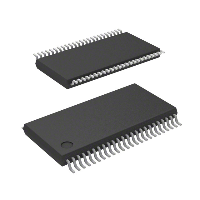
• Available in 48-pin SSOP
Key Specifications
CPU Cycle-to-cycle Jitter: .......................................... 250 ps
• Vendor ID and Revision ID support
CPU to CPU Output Skew........................................... 175 ps
• Programmable drive strength for CPU and PCI output
clocks
PCI Cycle-to-cycle Jitter: ............................................. 500 ps
• Programmable output skew between CPU, AGP and PCI
PCI to PCI Output Skew:............................................. 500 ps
Pin Configuration[1]
Block Diagram
Note:
1. Signals marked with * have internal pull-up resistors
......................... Document #: 38-07703 Rev. ** Page 1 of 18
400 West Cesar Chavez, Austin, TX 78701
1+(512) 416-8500
1+(512) 416-9669
www.silabs.com
�W311
Pin Definitions
Pin Name
Pin
Type
Pin No.
Pin Description
RST#
CPU1:3
32
39, 38, 35
O
(open
drain)
O
System Reset Output: Open-drain system reset output.
CPU Clock Output: Frequency is set by the FS0:4 input or through serial input
interface. The CPU1:3 outputs are gated by the CLK_STOP# input.
CPU_STOP#
34
I
CPU Output Control: 3.3V LVTTL-compatible input that stop CPU1:3.
PCI1:8
10, 11, 13,
14, 16, 17,
18, 20
O
PCI Clock Outputs 1 through 8: Frequency is set by FS0:4 inputs or through
serial input interface; see Table 5 for details. PCI1:8 outputs are gated by the
PCI_STOP# input.
PCI_STOP#
33
O
PCI_STOP# Input: 3.3V LVTTL-compatible input that stops PCI1:8.
PCI_F
9
O
Free-Running PCI Clock Output: Frequency is set by FS0:4 inputs or through
serial input interface; see Table 5 for details.
FS0:1
AGP0:2
21, 22
23, 26, 27
I
O
Frequency Selection Inputs: Selects CPU clock frequency as shown in Table 1.
AGP Clock Output: This pin serves as the select strap to determine device
operating frequency as described in Table 5.
APIC0:2
48MHz/FS3
45, 44, 42
6
O
I/O
APIC Clock Output: APIC clock outputs.
48 MHz Output/Frequency Select 3: 48 MHz is provided in normal operation.
In standard PC systems, this output can be used as the reference for the Universal
Serial Bus host controller. This pin also serves as a power-on strap option to
determine device operating frequency as described in Table 5.
24_48MHz/
FS2
REF1/FS4
7
47
I/O
I/O
24_48 MHz Output/Frequency Select 2: In standard PC systems, this output
can be used as the clock input for a Super I/O chip. The output frequency is
controlled by Configuration Byte 3 bit[6]. The default output frequency is 24 MHz.
This pin also serves as a power-on strap option to determine device operating
frequency as described in Table 5.
Reference Clock Output 1/Frequency Select 4: 3.3V 14.318 MHz output clock.
This pin also serves as a power-on strap option to determine device operating
frequency as described in Table 5.
REF0
48
O
Reference Clock Output 0: 3.3V 14.318 MHz output clock.
SCLK
28
I
Clock pin for SMBus circuitry.
SDATA
29
I/O
Data pin for SMBus circuitry.
X1
3
I
Crystal Connection or External Reference Frequency Input: This pin has dual
functions. It can be used as an external 14.318 MHz crystal connection or as an
external reference frequency input.
X2
41
I
Crystal Connection: An input connection for an external 14.318 MHz crystal. If
using an external reference, this pin must be left unconnected.
VDD_REF,
VDD_48MHz,
VDD_PCI,
VDD_AGP,
VDD_CORE
1, 5,15, 24,
31
P
VDD_CPU,
VDD_APIC
41, 46, 37
P
Power Connection: Power supply for core logic, PLL circuitry, PCI outputs,
reference outputs, 48 MHz output, and 24-48 MHz output, connect to 3.3V supply.
Power Connection: Power supply for APIC and CPU output buffers, connect to
2.5V.
.........................Document #: 38-07703 Rev. ** Page 2 of 18
�W311
Serial Data Interface
The W311 features a two-pin, serial data interface that can be
used to configure internal register settings that control
particular device functions.
Data Protocol
The clock driver serial protocol supports byte/word write,
byte/word read, block write and block read operations from the
controller. For block write/read operation, the bytes must be
accessed in sequential order from lowest to highest byte with
the ability to stop after any complete byte has been transferred. For byte/word write and byte read operations, system
controller can access individual indexed byte. The offset of the
indexed byte is encoded in the command code.
The definition for the command code is defined in Table 2.
Table 1.
Bit
Descriptions
7
0 = Block read or block write operation
1 = Byte/Word read or byte/word write operation
6:0
Byte offset for byte/word read or write operation. For block read or write operations, these bits
need to be set at ‘0000000’.
Table 2. Block Read and Block Write Protocol
Block Write Protocol
Bit
1
2:8
Description
Start
Slave address – 7 bits
Block Read Protocol
Bit
1
2:8
Description
Start
Slave address – 7 bits
9
Write
9
Write
10
Acknowledge from slave
10
Acknowledge from slave
11:18
19
20:27
28
29:36
37
38:45
Command Code – 8 bits
‘00000000’ stands for block operation
Acknowledge from slave
Byte Count – 8 bits
Acknowledge from slave
11:18
19
20
21:27
Command Code – 8 bits
‘00000000’ stands for block operation
Acknowledge from slave
Repeat start
Slave address – 7 bits
Data byte 0 – 8 bits
28
Read
Acknowledge from slave
29
Acknowledge from slave
Data byte 1 – 8 bits
46
Acknowledge from slave
...
Data Byte N/Slave Acknowledge...
...
Data Byte N – 8 bits
...
Acknowledge from slave
...
Stop
.........................Document #: 38-07703 Rev. ** Page 3 of 18
30:37
38
39:46
47
48:55
Byte count from slave – 8 bits
Acknowledge
Data byte from slave – 8 bits
Acknowledge
Data byte from slave – 8 bits
56
Acknowledge
...
Data bytes from slave/Acknowledge
...
Data byte N from slave – 8 bits
...
Not Acknowledge
...
Stop
�W311
Table 3. Word Read and Word Write Protocol
Word Write Protocol
Bit
1
2:8
9
10
11:18
19
20:27
Description
Start
Word Read Protocol
Bit
1
Slave address – 7 bits
Write
Acknowledge from slave
Command Code – 8 bits
‘1xxxxxxx’ stands for byte or word operation
bit[6:0] of the command code represents the
offset of the byte to be accessed
2:8
Description
Start
Slave address – 7 bits
9
Write
10
Acknowledge from slave
11:18
Command Code – 8 bits
‘1xxxxxxx’ stands for byte or word operation
bit[6:0] of the command code represents the
offset of the byte to be accessed
Acknowledge from slave
19
Acknowledge from slave
Data byte low – 8 bits
20
Repeat start
28
Acknowledge from slave
21:27
29:36
Data byte high –- 8 bits
28
Read
29
Acknowledge from slave
37
Acknowledge from slave
38
Stop
30:37
38
39:46
Slave address – 7 bits
Data byte low from slave – 8 bits
Acknowledge
Data byte high from slave – 8 bits
47
NOT acknowledge
48
Stop
Table 4. Byte Read and Byte Write Protocol
Byte Write Protocol
Bit
1
2:8
9
10
11:18
19
20:27
Description
Start
Slave address – 7 bits
Write
Acknowledge from slave
Command Code – 8 bits
‘1xxxxxxx’ stands for byte operation
bit[6:0] of the command code represents the
offset of the byte to be accessed
Byte Read Protocol
Bit
1
2:8
Description
Start
Slave address – 7 bits
9
Write
10
Acknowledge from slave
11:18
Command Code – 8 bits
‘1xxxxxxx’ stands for byte operation
bit[6:0] of the command code represents the
offset of the byte to be accessed
Acknowledge from slave
19
Acknowledge from slave
Data byte – 8 bits
20
Repeat start
28
Acknowledge from slave
29
Stop
21:27
28
29
30:37
.........................Document #: 38-07703 Rev. ** Page 4 of 18
Slave address – 7 bits
Read
Acknowledge from slave
Data byte from slave – 8 bits
38
Not Acknowledge
39
Stop
�W311
W311 Serial Configuration Map
2. All unused register bits (reserved and N/A) should be
written to a “0” level.
1. The serial bits will be read by the clock driver in the following
order:
3. All register bits labeled “Initialize to 0" must be written to
zero during initialization.
Byte 0 - Bits 7, 6, 5, 4, 3, 2, 1, 0
Byte 1 - Bits 7, 6, 5, 4, 3, 2, 1, 0
Byte N - Bits 7, 6, 5, 4, 3, 2, 1, 0
Byte 0: Control Register 0
Bit
Pin#
Bit 7
Name
Default
Description
–
Reserved
0
Reserved
Bit 6
–
SEL2
0
See Table 5
Bit 5
–
SEL1
0
See Table 5
Bit 4
–
SEL0
0
See Table 5
Bit 3
–
FS_Override
0
0 = Select operating frequency by FS[4:0] input pins
1 = Select operating frequency by SEL[4:0] settings
Bit 2
–
SEL4
1
See Table 5
Bit 1
–
SEL3
0
See Table 5
Bit 0
–
Reserved
0
Reserved
Byte 1: Control Register 1
Bit
Pin#
Name
Default
Description
Bit 7
-
Reserved
0
Reserved
Bit 6
-
Spread Select2
0
Bit 5
-
Spread Select1
0
Bit 4
-
Spread Select0
0
‘000’ = Normal (spread off)
‘001’ = Test Mode
‘010’ = Reserved
‘011’ = Three-Stated
‘100’ = –0.5%
‘101’ = ± 0.5%
‘110’ = ± 0.25%
‘111’ = ± 0.38%
Bit 3
35
CPU3
1
(Active/Inactive)
Bit 2
38
CPU2
1
(Active/Inactive)
Bit 1
39
CPU1
1
(Active/Inactive)
Bit 0
42
APIC2
1
(Active/Inactive)
Byte 2: Control Register 2
Bit
Pin#
Name
Default
Description
Bit 7
20
PC8
1
(Active/Inactive)
Bit 6
18
PCI7
1
(Active/Inactive)
Bit 5
17
PCI6
1
(Active/Inactive)
Bit 4
16
PCI5
1
(Active/Inactive)
Bit 3
14
PCI4
1
(Active/Inactive)
Bit 2
13
PCI3
1
(Active/Inactive)
Bit 1
11
PCI2
1
(Active/Inactive)
Bit 0
10
PCI1
1
(Active/Inactive)
.........................Document #: 38-07703 Rev. ** Page 5 of 18
�W311
Byte 3: Control Register
Bit
Pin#
Name
Default
Description
Bit 7
--
Reserved
0
Reserved
Bit 6
7
SEL_48MHz
0
0 = Select 24 MHz as output
1 = Select 48 MHz as output (default).
Bit 5
6
48MHz
1
(Active/Inactive)
Bit 4
7
24_48MHz
1
(Active/Inactive)
Bit 3
9
PCI_F
1
(Active/Inactive)
Bit 2
27
AGP2
1
(Active/Inactive)
Bit 1
26
AGP1
1
(Active/Inactive)
Bit 0
23
AGP0
1
(Active/Inactive)
Byte 4: Watchdog Timer Register
Bit
Pin#
Name
Default
Description
Bit 7
-
PCI_Skew1
0
PCI skew control
00 = Normal
01 = –500 ps
10 = Reserved
11 = +500 ps
Bit 6
-
PCI_Skew0
0
Bit 4
-
WD_TIMER4
1
Bit 3
-
WD_TIMER3
1
Bit 2
-
WD_TIMER2
1
Bit 1
-
WD_TIMER1
1
These bits store the time-out value of the Watchdog
Timer. The scale of the timer is determine by the pre
scaler.
The timer can support a value of 150 ms to 4.8 sec
when the pre-scalar is set to 150 ms. If the pre-scaler
is set to 2.5 sec, it can support a value from 2.5 sec
to 80 sec.
When the Watchdog Timer reaches to “0”, it will set
the WD_To_STATUS bit and generate Reset if
RST_EN_WD is enabled
Bit 0
-
WD_TIMER0
1
Bit 5
0 = 150 ms
1 = 2.5 sec
Byte 5: Control Register 5
Bit
Pin#
Name
Default
Description
Bit 7
6
48Mhz_DRV
1
0 = Norm, 1 = High Drive
Bit 6
7
24_48MHz_DRV
1
0 = Norm, 1 = High Drive
Bit 5
44
APIC1
1
(Active/Inactive)
Bit 4
45
APIC0
1
(Active/Inactive)
Bit 3
-
Reserved
0
Reserved
Bit 2
-
Reserved
0
Reserved
Bit 1
47
REF1
1
(Active/Inactive)
Bit 0
48
REF0
1
(Active/Inactive)
.........................Document #: 38-07703 Rev. ** Page 6 of 18
�W311
Byte 6: Reserved Register
Bit
Name
Default
Pin Description
Bit 7
Reserved
1
Reserved
Bit 6
Reserved
1
Reserved
Bit 5
Reserved
1
Reserved
Bit 4
Reserved
1
Reserved
Bit 3
Reserved
1
Reserved
Bit 2
Reserved
1
Reserved
Bit 1
Reserved
1
Reserved
Bit 0
Reserved
1
Reserved
Byte 7: Reserved Register
Bit
Name
Default
Pin Description
Bit 7
Reserved
1
Reserved
Bit 6
Reserved
1
Reserved
Bit 5
Reserved
1
Reserved
Bit 4
Reserved
1
Reserved
Bit 3
Reserved
1
Reserved
Bit 2
Reserved
1
Reserved
Bit 1
Reserved
1
Reserved
Bit 0
Reserved
1
Reserved
Byte 8: Vendor ID and Revision ID Register (Read Only)
Bit
Name
Default
Pin Description
Bit 7
Revision_ID3
0
Revision ID bit[3]
Bit 6
Revision_ID2
0
Revision ID bit[2]
Bit 5
Revision_ID1
0
Revision ID bit[1]
Bit 4
Revision_ID0
0
Revision ID bit[0]
Bit 3
Vendor_ID3
1
Bit[3] of Cypress Semiconductor’s Vendor ID. This bit is read only.
Bit 2
Vendor_ID2
0
Bit[2] of Cypress Semiconductor’s Vendor ID. This bit is read only.
Bit 1
Vendor _ID1
0
Bit[1] of Cypress Semiconductor’s Vendor ID. This bit is read only.
Bit 0
Vendor _ID0
0
Bit[0] of Cypress Semiconductor’s Vendor ID. This bit is read only.
.........................Document #: 38-07703 Rev. ** Page 7 of 18
�W311
Byte 9: System Reset and Watchdog Timer Register
Bit
Name
Default
Pin Description
Bit 7
Reserved
0
Reserved
Bit 6
PCI_DRV
0
PCI clock output drive strength
0 = Normal
1 = High Drive
Bit 5
Reserved
0
Reserved
Bit 4
RST_EN_WD
0
This bit will enable the generation of a Reset pulse when a watchdog timer
time-out occurs.
0 = Disabled
1 = Enabled
Bit 3
RST_EN_FC
0
This bit will enable the generation of a Reset pulse after a frequency change
occurs.
0 = Disabled
1 = Enabled
Bit 2
WD_TO_STATU
S
0
Watchdog Timer Time-out Status bit
0 = No time-out occurs (READ); Ignore (WRITE)
1 = time-out occurred (READ); Clear WD_TO_STATUS (WRITE)
Bit 1
WD_EN
0
0 = Stop and re-load Watchdog Timer
1 = Enable Watchdog Timer. It will start counting down after a frequency
change occurs.
Note: W311 will generate system reset, reload a recovery frequency, and lock
itself into a recovery frequency mode after a watchdog timer time-out occurs.
Under recovery frequency mode, W311 will not respond to any attempt to
change output frequency via the SMBus control bytes. System software can
unlock W311 from its recovery frequency mode by clearing the WD_EN bit.
Bit 0
Reserved
0
Reserved
Byte 10: Skew Control Register
Bit
Name
Default
Description
Bit 7
CPU_Skew2
0
Bit 6
CPU_Skew1
0
Bit 5
CPU_Skew0
0
Bit 4
Reserved
0
Reserved
Bit 3
Reserved
0
Reserved
Bit 2
Reserved
0
Reserved
AGP skew control
00 = Normal
01 = –150 ps
10 = +150 ps
11 = +300 ps
Bit 1
AGP_Skew1
0
Bit 0
AGP_Skew0
0
CPU skew control
000 = Normal
001 = –150 ps
010 = –300 ps
011 = –450 ps
100 = +150 ps
101 = +300 ps
110 = +450 ps
111 = +600 ps
.........................Document #: 38-07703 Rev. ** Page 8 of 18
�W311
Byte 11: Recovery Frequency N - Value Register
Bit
Name
Default
Description
If ROCV_FREQ_SEL is set, W311 will use the values programmed in ROCV_FREQ_N[7:0] and ROCV_FREQ_M[6:0] to determine the recovery CPU output
frequency.when a Watchdog Timer time-out occurs.
The setting of FS_Override bit determines the frequency ratio for CPU, SDRAM,
AGP and SDRAM. When it is cleared, W311 will use the same frequency ratio
stated in the Latched FS[4:0] register. When it is set, W311 will use the
frequency ratio stated in the SEL[4:0] register.
W312 supports programmable CPU frequency ranging from 50 MHz to 248
MHz.
W311 will change the output frequency whenever there is an update to either
ROCV_FREQ_N[7:0] and ROCV_FREQ_M[6:0]. Therefore, it is recommended
to use Word or Block write to update both registers within the same SMBus bus
operation.
Bit 7
ROCV_FREQ_N7
0
Bit 6
ROCV_FREQ_N6
0
Bit 5
ROCV_FREQ_N5
0
Bit 4
ROCV_FREQ_N4
0
Bit 3
ROCV_FREQ_N3
0
Bit 2
ROCV_FREQ_N2
0
Bit 1
ROCV_FREQ_N1
0
Bit 0
ROCV_FREQ_N0
0
Byte 12: Recovery Frequency M- Value Register
Bit
Name
Default
Pin Description
Bit 7
ROCV_FREQ_SEL
0
ROCV_FREQ_SEL determines the source of the recover frequency when a
Watchdog Timer time-out occurs. The clock generator will automatically
switch to the recovery CPU frequency based on the selection on ROCV_FREQ_SEL.
0 = From latched FS[4:0]
1 = From the settings of ROCV_FREQ_N[7:0] & ROCV_FREQ_M[6:0]
Bit 6
ROCV_FREQ_M6
0
Bit 5
ROCV_FREQ_M5
0
Bit 4
ROCV_FREQ_M4
0
Bit 3
ROCV_FREQ_M3
0
Bit 2
ROCV_FREQ_M2
0
Bit 1
ROCV_FREQ_M1
0
If ROCV_FREQ_SEL is set, W311 will use the values programmed in ROCV_FREQ_N[7:0] and ROCV_FREQ_M[6:0] to determine the recovery CPU
output frequency.when a Watchdog Timer time-out occurs.The setting of
FS_Override bit determines the frequency ratio for CPU, SDRAM, AGP and
SDRAM. When it is cleared, W311 will use the same frequency ratio stated in
the Latched FS[4:0] register. When it is set, W311 will use the frequency ratio
stated in the SEL[4:0] register. W311 supports programmable CPU frequency
ranging from 50 MHz to 248 MHz.
Bit 0
ROCV_FREQ_M0
0
Byte 13: Programmable Frequency Select N-Value Register
Default
Pin Description
Bit 7
Bit
CPU_FSEL_N7
Name
0
Bit 6
CPU_FSEL_N6
0
Bit 5
CPU_FSEL_N5
0
Bit 4
CPU_FSEL_N4
0
Bit 3
CPU_FSEL_N3
0
Bit 2
CPU_FSEL_N2
0
If Prog_Freq_EN is set, W311 will use the values programmed in CPU_FSEL_N[7:0] and CPU_FSEL_M[6:0] to determine the CPU output frequency.
The new frequency will start to load whenever CPU_FSELM[6:0] is updated.
The setting of FS_Override bit determines the frequency ratio for CPU,
SDRAM, AGP and SDRAM. When it is cleared, W311 will use the same
frequency ratio stated in the Latched FS[4:0] register. When it is set, W311
will use the frequency ratio stated in the SEL[4:0] register. W311 supports
programmable CPU frequency ranging from 50 MHz to 248 MHz.
Bit 1
CPU_FSEL_N1
0
Bit 0
CPU_FSEL_N0
0
.........................Document #: 38-07703 Rev. ** Page 9 of 18
�W311
Byte 14: Programmable Frequency Select N-Value Register
Bit
Name
Default
Description
Bit 7
Pro_Freq_EN
0
Programmable output frequencies enabled
0 = disabled
1 = enabled
Bit 6
CPU_FSEL_M6
0
Bit 5
CPU_FSEL_M5
0
Bit 4
CPU_FSEL_M4
0
Bit 3
CPU_FSEL_M3
0
Bit 2
CPU_FSEL_M2
0
If Prog_Freq_EN is set, W311 will use the values programmed in CPU_FSEL_N[7:0] and CPU_FSEL_M[6:0] to determine the CPU output frequency.
The new frequency will start to load whenever CPU_FSELM[6:0] is updated.
The setting of FS_Override bit determines the frequency ratio for CPU,
SDRAM, AGP and SDRAM. When it is cleared, W311 will use the same
frequency ratio stated in the Latched FS[4:0] register. When it is set, W311
will use the frequency ratio stated in the SEL[4:0] register.
Bit 1
CPU_FSEL_M1
0
Bit 0
CPU_FSEL_M0
0
Byte 15: Reserved Register
Bit
Pin#
Name
Default
Description
Bit 7
47
Latched FS4 input
X
Bit 6
6
Latched FS3 input
X
Bit 5
7
Latched FS2 input
X
Bit 4
21
Latched FS1 input
X
Bit 3
22
Latched FS0 input
X
Bit 2
-
Vendor test mode
0
Reserved. Write with ‘0’
Bit 1
-
Vendor test mode
1
Reserved. Write with ‘1’
Bit 0
-
Vendor test mode
1
Reserved. Write with ‘1’
Latched FS[4:0] inputs. These bits are read only.
Byte 16: Reserved Register
Pin#
Name
Default
Bit 7
Bit
-
Vendor test mode
0
Reserved. Write with ‘0’.
Description
Bit 6
-
Vendor test mode
0
Reserved. Write with ‘0’.
Bit 5
-
Vendor test mode
0
Reserved. Write with ‘0’.
Bit 4
-
Vendor test mode
0
Reserved. Write with ‘0’.
Bit 3
-
Vendor test mode
0
Reserved. Write with ‘0’.
Bit 2
-
Vendor test mode
0
Reserved. Write with ‘0’.
Bit 1
-
Vendor test mode
0
Reserved. Write with ‘0’.
Bit 0
-
Vendor test mode
0
Reserved. Write with ‘0’.
Byte 17: Reserved Register
Pin#
Name
Default
Bit 7
Bit
-
Vendor test mode
0
Reserved. Write with ‘0’.
Bit 6
-
Vendor test mode
0
Reserved. Write with ‘0’.
Bit 5
-
Vendor test mode
0
Reserved. Write with ‘0’.
Bit 4
-
Vendor test mode
0
Reserved. Write with ‘0’.
Bit 3
-
Vendor test mode
0
Reserved. Write with ‘0’.
Bit 2
-
Vendor test mode
0
Reserved. Write with ‘0’.
Bit 1
-
Vendor test mode
0
Reserved. Write with ‘0’.
Bit 0
-
Vendor test mode
0
Reserved. Write with ‘0’.
.......................Document #: 38-07703 Rev. ** Page 10 of 18
Description
�W311
Table 5. Additional Frequency Selections through Serial Data Interface Data Bytes
Input Conditions
Output Frequency
FS4
FS3
FS2
FS1
FS0
SEL4
SEL3
SEL2
SEL1
SEL0
CPU
3V66
PCI
PLL Gear
Constants
(G)
0
0
0
0
0
200.0
66.6
33.3
48.00741
0
0
0
0
1
190.0
76.0
38.0
48.00741
0
0
0
1
0
180.0
72.0
36.0
48.00741
0
0
0
1
1
170.0
68.0
34.0
48.00741
0
0
1
0
0
166.0
66.4
33.2
48.00741
0
0
1
0
1
160.0
64.0
32.0
48.00741
0
0
1
1
0
150.0
75.0
37.5
48.00741
0
0
1
1
1
145.0
72.5
36.3
48.00741
0
1
0
0
0
140.0
70.0
35.0
48.00741
0
1
0
0
1
136.0
68.0
34.0
48.00741
0
1
0
1
0
130.0
65.0
32.5
48.00741
0
1
0
1
1
124.0
62.0
31.0
48.00741
0
1
1
0
0
66.6
66.6
33.3
48.00741
0
1
1
0
1
100.0
66.6
33.3
48.00741
0
1
1
1
0
118.0
78.7
39.3
48.00741
0
1
1
1
1
133.3
66.6
33.3
48.00741
1
0
0
0
0
66.8
66.8
33.4
48.00741
1
0
0
0
1
100.2
66.8
33.4
48.00741
1
0
0
1
0
115.0
76.7
38.3
48.00741
1
0
0
1
1
133.6
66.8
33.4
48.00741
1
0
1
0
0
66.8
66.8
33.4
48.00741
1
0
1
0
1
100.2
66.8
33.4
48.00741
1
0
1
1
0
110.0
73.3
36.7
48.00741
1
0
1
1
1
133.6
66.8
33.4
48.00741
1
1
0
0
0
105.0
70.0
35.0
48.00741
1
1
0
0
1
90.0
60.0
30.0
48.00741
1
1
0
1
0
85.0
56.7
28.3
48.00741
1
1
0
1
1
78.0
78.0
39.0
48.00741
1
1
1
0
0
66.6
66.6
33.3
48.00741
1
1
1
0
1
100.0
66.6
33.3
48.00741
1
1
1
1
0
75.0
75.0
37.5
48.00741
1
1
1
1
1
133.3
66.6
33.3
48.00741
Programmable Output Frequency, Watchdog Timer and
Recovery Output Frequency Functional Description
The Programmable Output Frequency feature allows users to
generate any CPU output frequency from the range of 50 MHz
to 248 MHz. Cypress offers the most dynamic and the simplest
programming interface for system developers to utilize this
feature in their platforms.
The Watchdog Timer and Recovery Output Frequency
features allow users to implement a recovery mechanism
when the system hangs or getting unstable. System BIOS or
other control software can enable the Watchdog timer before
they attempt to make a frequency change. If the system hangs
and a Watchdog timer time-out occurs, a system reset will be
generated and a recovery frequency will be activated.
All of the related registers are summarized inTable 7.
....................... Document #: 38-07703 Rev. ** Page 11 of 18
�W311
Table 6. Register Summary
Name
Description
Pro_Freq_EN
Programmable output frequencies enabled
0 = Disabled (default)
1 = Enabled
When it is disabled, the operating output frequency will be determined by either the latched value of
FS[4:0] inputs or the programmed value of SEL[4:0]. If FS_Override bit is clear, latched FS[4:0] inputs
will be used. If FS_Override bit is set, programmed value of SEL[4:0] will be used.
When it is enabled, the CPU output frequency will be determined by the programmed value of
CPUFSEL_N, CPUFSEL_M and the PLL Gear Constant. The program value of FS_Override, SEL[4:0]
or the latched value of FS[4:0] will determine the PLL Gear Constant and the frequency ratio between
CPU and other frequency outputs.
FS_Override
When Pro_Freq_EN is cleared or disabled,
0 = Select operating frequency by FS input pins (default)
1 = Select operating frequency by SEL bits in SMBus control bytes
When Pro_Freq_EN is set or enabled,
0 = Frequency output ratio between CPU and other frequency groups and the PLL Gear Constant are
based on the latched value of FS input pins (default)
1 = Frequency output ratio between CPU and other frequency groups and the PLL Gear Constant are
based on the programmed value of SEL bits in SMBus control bytes
CPU_FSEL_N,
CPU_FSEL_M
ROCV_FREQ_SEL
When Prog_Freq_EN is set or enabled, the values programmed in CPU_FSEL_N[7:0] and CPU_FSEL_M[6:0] determines the CPU output frequency. The new frequency will start to load whenever there
is an update to either CPU_FSEL_N[7:0] or CPU_FSEL_M[6:0]. Therefore, it is recommended to use
Word or Block write to update both registers within the same SMBus bus operation.
The setting of FS_Override bit determines the frequency ratio for CPU, AGP and PCI. When
FS_Override is cleared or disabled, the frequency ratio follows the latched value of the FS input pins.
When FS_Override is set or enabled, the frequency ratio follows the programmed value of SEL bits in
SMBus control bytes.
ROCV_FREQ_SEL determines the source of the recover frequency when a Watchdog Timer timeout
occurs. The clock generator will automatically switch to the recovery CPU frequency based on the
selection on ROCV_FREQ_SEL.
0 = From latched FS[4:0]
1 = From the settings of ROCV_FREQ_N[7:0] & ROCV_FREQ_M[6:0]
ROCV_FREQ_N[7:0],
ROCV_FREQ_M[6:0]
When ROCV_FREQ_SEL is set, the values programmed in ROCV_FREQ_N[7:0] and ROCV_FREQ_M[6:0] will be used to determine the recovery CPU output frequency when a Watchdog Timer
time-out occurs
The setting of FS_Override bit determines the frequency ratio for CPU, AGP and PCI. When it is cleared,
the same frequency ratio stated in the Latched FS[4:0] register will be used.
When it is set, the frequency ratio stated in the SEL[4:0] register will be used.
The new frequency will start to load whenever there is an update to either ROCV_FREQ_N[7:0] and
ROCV_FREQ_M[6:0]. Therefore, it is recommended to use word or block write to update both registers
within the same SMBus bus operation.
WD_EN
0 = Stop and reload Watchdog Timer
1 = Enable Watchdog Timer. It will start counting down after a frequency change occurs.
Pro_Freq_EN
Programmable output frequencies enabled
0 = Disabled (default)
1 = Enabled
When it is disabled, the operating output frequency will be determined by either the latched value of
FS[4:0] inputs or the programmed value of SEL[4:0]. If FS_Override bit is clear, latched FS[4:0] inputs
will be used. If FS_Override bit is set, programmed value of SEL[4:0] will be used.
When it is enabled, the CPU output frequency will be determined by the programmed value of
CPUFSEL_N, CPUFSEL_M and the PLL Gear Constant. The program value of FS_Override, SEL[4:0]
or the latched value of FS[4:0] will determine the PLL Gear Constant and the frequency ratio between
CPU and other frequency outputs.
.......................Document #: 38-07703 Rev. ** Page 12 of 18
�W311
Table 6. Register Summary (continued)
Name
Description
FS_Override
When Pro_Freq_EN is cleared or disabled,
0 = Select operating frequency by FS input pins (default)
1 = Select operating frequency by SEL bits in SMBus control bytes
When Pro_Freq_EN is set or enabled,
0 = Frequency output ratio between CPU and other frequency groups and the PLL Gear Constant are
based on the latched value of FS input pins (default)
1 = Frequency output ratio between CPU and other frequency groups and the PLL Gear Constant are
based on the programmed value of SEL bits in SMBus control bytes
CPU_FSEL_N,
CPU_FSEL_M
ROCV_FREQ_SEL
When Prog_Freq_EN is set or enabled, the values programmed in CPU_FSEL_N[7:0] and CPU_FSEL_M[6:0] determines the CPU output frequency. The new frequency will start to load whenever there
is an update to either CPU_FSEL_N[7:0] or CPU_FSEL_M[6:0]. Therefore, it is recommended to use
Word or Block write to update both registers within the same SMBus bus operation.
The setting of FS_Override bit determines the frequency ratio for CPU, AGP and PCI. When
FS_Override is cleared or disabled, the frequency ratio follows the latched value of the FS input pins.
When FS_Override is set or enabled, the frequency ratio follows the programmed value of SEL bits in
SMBus control bytes.
ROCV_FREQ_SEL determines the source of the recover frequency when a Watchdog Timer timeout
occurs. The clock generator will automatically switch to the recovery CPU frequency based on the
selection on ROCV_FREQ_SEL.
0 = From latched FS[4:0]
1 = From the settings of ROCV_FREQ_N[7:0] & ROCV_FREQ_M[6:0]
WD_PRE_SCALER
0 = 150 ms
1 = 2.5 sec
RST_EN_WD
This bit will enable the generation of a Reset pulse when a Watchdog timer time-out occurs.
0 = Disabled
1 = Enabled
RST_EN_FC
This bit will enable the generation of a Reset pulse after a frequency change occurs.
0 = Disabled
1 = Enabled
How to Program CPU Output Frequency
When the programmable output frequency feature is enabled
(Pro_Freq_EN bit is set), the CPU output frequency is determined by the following equation:
Fcpu = G * (N+3)/(M+3)
“N” and “M” are the values programmed in Programmable
Frequency Select N-Value Register and M-Value Register,
respectively.
“G” stands for the PLL Gear Constant, which is determined by
the programmed value of FS[4:0] or SEL[4:0]. The value is
listed in Table 5. The ratio of (N+3) and (M+3) need to be
greater than “1” [(N+3)/(M+3) > 1].
Table 7 lists set of N and M values for different frequency
output ranges.This example use a fixed value for the M-Value
Register and select the CPU output frequency by changing the
value of the N-Value Register.
Table 7. Examples of N and M Value for Different CPU Frequency Range
Frequency Ranges
Gear Constants
Fixed Value for
M-Value Register
Range of N-Value Register
for Different CPU Frequency
50 MHz–129 MHz
48.00741
93
97–255
130 MHz–248 MHz
48.00741
45
127–245
.......................Document #: 38-07703 Rev. ** Page 13 of 18
�W311
Absolute Maximum Ratings[2]
tions above those specified in the operating sections of this
specification is not implied. Maximum conditions for extended
periods may affect reliability.
Stresses greater than those listed in this table may cause
permanent damage to the device. These represent a stress
rating only. Operation of the device at these or any other condi.
Rating
Unit
VDD, VIN
Parameter
Voltage on any pin with respect to GND
Description
–0.5 to +7.0
V
TSTG
Storage Temperature
–65 to +150
°C
TB
Ambient Temperature under Bias
–55 to +125
°C
TA
Operating Temperature
0 to +70
°C
ESDPROT
Input ESD Protection
2 (min.)
kV
DC Electrical Characteristics: TA = 0°C to +70°C, VDD = 3.3V±5% and 2.5V±5%
Parameter
Description
Test Condition
Min.
Typ.
Max.
Unit
–
260
–
mA
–
25
–
mA
Supply Current
IDD
3.3V Supply Current
IDD
2.5V Supply Current
CPU [1:3]=133 MHz[3]
Logic Inputs
VIL
Input Low Voltage
GND – 0.3
–
0.8
V
VIH
Input High Voltage
2.0
–
VDD + 0.3
V
IIL
Input Low
Current[4]
–
–
–25
µA
IIH
Input High Current[4]
–
–
10
µA
–
–
50
mV
IOH = –1 mA
3.1
–
–
V
IOH = –1 mA
2.2
–
–
V
Clock Outputs
VOL
Output Low Voltage
VOH
Output High Voltage
VOH
Output Low Voltage
IOL
Output Low Current
IOH
Output High Current
IOL = 1 mA
CPUT[1:3]
APIC[0:2]
CPU1:3
VOL = 1.25V
27
57
97
mA
PCI_F, PCI1:8
VOL = 1.5V
20.5
53
139
mA
AGP0:2
VOL = 1.25V
40
85
140
mA
APIC0:2
VOL = 1.25V
40
85
140
mA
REF0:1
VOL = 1.5V
25
37
76
mA
48-MHz
VOL = 1.5V
25
37
76
mA
24-MHz
VOL = 1.5V
25
37
76
mA
CPU1:3
VOH = 1.25V
25
55
97
mA
PCI_F, PCI1:8
VOH = 1.5V
31
55
139
mA
AGP0:2
VOL = 1.25V
40
85
140
mA
APIC0:1
VOH = 1.5V
27
44
94
mA
48-MHz
VOH = 1.5V
27
44
94
mA
24-MHz
VOH = 1.5V
25
37
76
mA
Notes:
2. Multiple Supplies: The voltage on any input or I/O pin cannot exceed the power pin during power-up. Power supply sequencing is NOT required.
3. All clock outputs loaded with 6" 60 transmission lines with 22-pF capacitors.
4. Inputs have internal pull-up resistors
.......................Document #: 38-07703 Rev. ** Page 14 of 18
�W311
DC Electrical Characteristics: TA = 0°C to +70°C, VDD = 3.3V±5% and 2.5V±5% (continued)
Parameter
Description
Test Condition
Min.
Typ.
Max.
Unit
–
1.65
–
V
–
18
–
pF
Pin X2 unconnected
–
28
–
pF
Except X1 and X2
–
–
5
pF
Crystal Oscillator
VTH
X1 Input Threshold Voltage[5]
CLOAD
Load Capacitance, Imposed on
External Crystal[6]
CIN,X1
X1 Input Capacitance[7]
VDD = 3.3V
Pin Capacitance/Inductance
CIN
Input Pin Capacitance
COUT
Output Pin Capacitance
–
–
6
pF
LIN
Input Pin Inductance
–
–
7
nH
AC Electrical Characteristics
TA = 0°C to +70°C, VDD = 3.3V±5%, VDD = 2.5V±5%fXTL = 14.31818 MHz
AC clock parameters are tested and guaranteed over stated operating conditions using the stated lump capacitive load at the
clock output; Spread Spectrum is disabled.
CPU Clock Outputs (Lump Capacitance Test Load = 20 pF)
Parameter
Description
Test Condition
/Comments
CPU = 66.6 MHz
CPU = 100 MHz
CPU = 133 MHz
Min. Typ. Max. Min. Typ. Max. Min. Typ. Max. Unit
tP
Period
Measured on rising edge at
1.25
15
–
15.5
10
–
10.5
7.5
–
8.0
ns
tH
High Time
Duration of clock cycle
above 2.0V
5.2
–
–
3.0
–
–
1.87
–
–
ns
tL
Low Time
Duration of clock cycle
below 0.4V
5.0
–
–
2.8
–
–
1.67
–
–
ns
tR
Output Rise Edge
Rate
Measured from 0.4V to
2.0V
1
–
4
1
–
4
1
–
4
V/ns
tF
Output Fall Edge
Rate
Measured from 2.0V to
0.4V
1
–
4
1
–
4
1
–
4
V/ns
tD
Duty Cycle
Measured on rising and
falling edge at 1.25V
45
–
55
45
–
55
45
–
55
%
tJC
Jitter,
Cycle-to-Cycle
Measured on rising edge at
1.25V. Maximum
difference of cycle time
between two adjacent
cycles.
–
–
250
–
–
250
–
–
250
ps
tSK
Output Skew
Measured on rising edge at
1.25V
–
–
175
–
–
175
–
–
175
ps
fST
Frequency
Assumes full supply
Stabilization from
voltage reached within
Power-up (cold start) 1 ms from power-up. Short
cycles exist prior to
frequency stabilization.
–
–
3
–
–
3
–
–
3
ms
Zo
AC Output
Impedance
–
20
–
–
20
–
–
20
–
Average value during
switching transition. Used
for determining series
termination value.
Notes:
5. X1 input threshold voltage (typical) is 3.3V/2
6. The W311 contains an internal crystal load capacitor between pin X1 and ground and another between pin X2 and ground. Total load placed on crystal is 18 pF;
this includes typical stray capacitance of short PCB traces to crystal.
7. X1 input capacitance is applicable when driving X1 with an external clock source (X2 is left unconnected).
.......................Document #: 38-07703 Rev. ** Page 15 of 18
�W311
PCI Clock Outputs (Lump Capacitance Test Load = 30 pF)
Parameter
Description
Test Condition/Comments
Min.
Typ.
Max.
Unit
tP
Period
Measured on rising edge at 1.5V
30
–
–
ns
tH
High Time
Duration of clock cycle above 2.4V
12
–
–
ns
tL
Low Time
Duration of clock cycle below 0.4V
12
–
–
ns
tR
Output Rise Edge Rate
Measured from 0.4V to 2.4V
1
–
4
V/ns
tF
Output Fall Edge Rate
Measured from 2.4V to 0.4V
1
–
4
V/ns
tD
Duty Cycle
Measured on rising and falling edge at 1.5V
45
–
55
%
tJC
Jitter, Cycle-to-Cycle
Measured on rising edge at 1.5V. Maximum
difference of cycle time between two adjacent cycles.
–
–
500
ps
tSK
Output Skew
Measured on rising edge at 1.5V
–
–
500
ps
tO
CPU to PCI Clock Skew
Covers all CPU/PCI outputs. Measured on rising
edge at 1.5V. CPU leads PCI output.
1.5
–
4
ns
fST
Frequency Stabilization
from Power-up (cold
start)
Assumes full supply voltage reached within 1 ms
from power-up. Short cycles exist prior to frequency
stabilization.
–
–
3
ms
Zo
AC Output Impedance
Average value during switching transition. Used for
determining series termination value.
–
30
–
Min.
Typ.
Max.
Unit
15
–
–
ns
AGP Clock Outputs (Lump Capacitance Test Load = 30 pF)
Parameter
Description
Test Condition/Comments
tP
Period
Measured on rising edge at 1.5V
tH
High Time
Duration of clock cycle above 2.4V
5.25
–
–
ns
tL
Low Time
Duration of clock cycle below 0.4V
5.05
–
–
ns
tR
Output Rise Edge Rate
Measured from 0.4V to 2.4V
1
–
4
V/ns
tF
Output Fall Edge Rate
Measured from 2.4V to 0.4V
1
–
4
V/ns
tD
Duty Cycle
Measured on rising and falling edge at 1.5V
45
–
55
%
tJC
Jitter, Cycle-to-Cycle
Measured on rising edge at 1.5V. Maximum
difference of cycle time between two adjacent
cycles.
–
–
500
ps
tSK
Output Skew
Measured on rising edge at 1.5V
–
–
250
ps
fST
Frequency Stabilization from
Power-up (cold start)
Assumes full supply voltage reached within
1 ms from power-up. Short cycles exist prior to
frequency stabilization.
–
–
3
ms
Zo
AC Output Impedance
Average value during switching transition. Used
for determining series termination value.
–
30
–
Min.
Typ.
Max.
Unit
APIC Clock Output (Lump Capacitance Test Load = 20 pF)
Parameter
Description
Test Condition/Comments
f
Frequency, Actual
Frequency generated from PCI divided by 2
tR
Output Rise Edge Rate
Measured from 0.4V to 2.4V
0.5
2
V/ns
tF
Output Fall Edge Rate
Measured from 2.4V to 0.4V
0.5
2
V/ns
tD
Duty Cycle
Measured on rising and falling edge at 1.5V
45
55
%
fST
Frequency Stabilization
from Power-up (cold start)
Assumes full supply voltage reached within 1 ms
from power-up. Short cycles exist prior to
frequency stabilization.
3
ms
Zo
AC Output Impedance
Average value during switching transition. Used
for determining series termination value.
.......................Document #: 38-07703 Rev. ** Page 16 of 18
PCI/2
40
MHz
�W311
REF Clock Output (Lump Capacitance Test Load = 20 pF)
Parameter
Description
Test Condition/Comments
Min.
Typ.
Max.
14.318
Unit
f
Frequency, Actual
Frequency generated by crystal oscillator
tR
Output Rise Edge Rate
Measured from 0.4V to 2.4V
0.5
–
2
MHz
V/ns
tF
Output Fall Edge Rate
Measured from 2.4V to 0.4V
0.5
–
2
V/ns
tD
Duty Cycle
Measured on rising and falling edge at 1.5V
45
–
55
%
fST
Frequency Stabilization
from Power-up (cold start)
Assumes full supply voltage reached within 1 ms
from power-up. Short cycles exist prior to
frequency stabilization.
–
–
3
ms
Zo
AC Output Impedance
Average value during switching transition. Used
for determining series termination value.
–
40
–
Min.
Typ.
Max.
Unit
48-MHz Clock Output (Lump Capacitance Test Load = 20 pF)
Parameter
Description
Test Condition/Comments
f
Frequency, Actual
Determined by PLL divider ratio (see m/n below)
48.008
MHz
fD
Deviation from 48 MHz
(48.008 – 48)/48
+167
ppm
m/n
PLL Ratio
(14.31818 MHz x 57/17 = 48.008 MHz)
tR
Output Rise Edge Rate
Measured from 0.4V to 2.4V
0.5
–
2
V/ns
tF
Output Fall Edge Rate
Measured from 2.4V to 0.4V
0.5
–
2
V/ns
tD
Duty Cycle
Measured on rising and falling edge at 1.5V
45
–
55
%
fST
Frequency Stabilization
from Power-up (cold start)
Assumes full supply voltage reached within 1 ms
from power-up. Short cycles exist prior to
frequency stabilization.
–
–
3
ms
Zo
AC Output Impedance
Average value during switching transition. Used
for determining series termination value.
–
40
–
Min.
Typ.
Max.
Unit
57/17
24-MHz Clock Output (Lump Capacitance Test Load = 20 pF)
Parameter
f
Description
Test Condition/Comments
Frequency, Actual
Determined by PLL divider ratio (see m/n below)
24.004
MHz
fD
Deviation from 24 MHz
m/n
PLL Ratio
(24.004 – 24)/24
+167
ppm
(14.31818 MHz x 57/34 = 24.004 MHz)
57/34
tR
Output Rise Edge Rate
Measured from 0.4V to 2.4V
0.5
–
2
V/ns
tF
Output Fall Edge Rate
Measured from 2.4V to 0.4V
0.5
–
2
V/ns
tD
Duty Cycle
Measured on rising and falling edge at 1.5V
45
–
55
%
fST
Frequency Stabilization
from Power-up (cold start)
Assumes full supply voltage reached within 1 ms
from power-up. Short cycles exist prior to
frequency stabilization.
–
–
3
ms
Zo
AC Output Impedance
Average value during switching transition. Used
for determining series termination value.
–
40
–a
.......................Document #: 38-07703 Rev. ** Page 17 of 18
�W311
Ordering Information
Ordering Code
Package Type
Product Flow
W311H
48-pin SSOP
Commercial, 0°C to 70°C
W311HT
48-pin SSOP - Tape and Reel
Commercial, 0°C to 70°C
CYW311OXC
48-pin SSOP
Commercial, 0°C to 70°C
CYW311OXCT
48-pin SSOP - Tape and Reel
Commercial, 0°C to 70°C
Lead-free
Package Drawing and Dimension
48-Lead Shrunk Small Outline Package O48
.......................Document #: 38-07703 Rev. ** Page 18 of 18
�ClockBuilder Pro
One-click access to Timing tools,
documentation, software, source
code libraries & more. Available for
Windows and iOS (CBGo only).
www.silabs.com/CBPro
Timing Portfolio
www.silabs.com/timing
SW/HW
www.silabs.com/CBPro
Quality
www.silabs.com/quality
Support and Community
community.silabs.com
Disclaimer
Silicon Laboratories intends to provide customers with the latest, accurate, and in-depth documentation of all peripherals and modules available for system and software implementers using
or intending to use the Silicon Laboratories products. Characterization data, available modules and peripherals, memory sizes and memory addresses refer to each specific device, and
"Typical" parameters provided can and do vary in different applications. Application examples described herein are for illustrative purposes only. Silicon Laboratories reserves the right to
make changes without further notice and limitation to product information, specifications, and descriptions herein, and does not give warranties as to the accuracy or completeness of the
included information. Silicon Laboratories shall have no liability for the consequences of use of the information supplied herein. This document does not imply or express copyright licenses
granted hereunder to design or fabricate any integrated circuits. The products are not designed or authorized to be used within any Life Support System without the specific written consent
of Silicon Laboratories. A "Life Support System" is any product or system intended to support or sustain life and/or health, which, if it fails, can be reasonably expected to result in significant
personal injury or death. Silicon Laboratories products are not designed or authorized for military applications. Silicon Laboratories products shall under no circumstances be used in
weapons of mass destruction including (but not limited to) nuclear, biological or chemical weapons, or missiles capable of delivering such weapons.
Trademark Information
Silicon Laboratories Inc.® , Silicon Laboratories®, Silicon Labs®, SiLabs® and the Silicon Labs logo®, Bluegiga®, Bluegiga Logo®, Clockbuilder®, CMEMS®, DSPLL®, EFM®, EFM32®,
EFR, Ember®, Energy Micro, Energy Micro logo and combinations thereof, "the world’s most energy friendly microcontrollers", Ember®, EZLink®, EZRadio®, EZRadioPRO®, Gecko®,
ISOmodem®, Precision32®, ProSLIC®, Simplicity Studio®, SiPHY®, Telegesis, the Telegesis Logo®, USBXpress® and others are trademarks or registered trademarks of Silicon Laboratories Inc. ARM, CORTEX, Cortex-M3 and THUMB are trademarks or registered trademarks of ARM Holdings. Keil is a registered trademark of ARM Limited. All other products or brand
names mentioned herein are trademarks of their respective holders.
Silicon Laboratories Inc.
400 West Cesar Chavez
Austin, TX 78701
USA
http://www.silabs.com
�