BLE112 DEVELOPMENT KIT 2.0
DATASHEET
Monday, 24 February 2014
Version 1.2
�Copyright © 2000-2014 Bluegiga Technologies
All rights reserved.
Bluegiga Technologies assumes no responsibility for any errors which may appear in this manual.
Furthermore, Bluegiga Technologies reserves the right to alter the hardware, software, and/or specifications
detailed here at any time without notice and does not make any commitment to update the information
contained here. Bluegiga’s products are not authorized for use as critical components in life support devices
or systems.
The WRAP is a registered trademark of Bluegiga Technologies
The Bluetooth trademark is owned by the Bluetooth SIG Inc., USA and is licensed to Bluegiga Technologies.
All other trademarks listed herein are owned by their respective owners.
Bluegiga Technologies Oy
�VERSION HISTORY
Version
Comment
1.2
Figure 2 added
1.1
Chapter 2.9: Using the Analog Comparator of BLE112 added
1.0
Release
Bluegiga Technologies Oy
�TABLE OF CONTENTS
1
Design Overview ...........................................................................................................................................5
1.1
2
Sensors, display and USB to UART converter .....................................................................................6
Interfaces .......................................................................................................................................................7
2.1
Powering the Development Board ........................................................................................................7
2.2
On-Board Debugger .............................................................................................................................7
2.2.1
Using the On-Board Debugger to Update the FW of the Embedded BLE112 Module ....................7
2.2.2
Using the On-Board Debugger to Update External Devices ............................................................7
2.3
Indicator LED ........................................................................................................................................8
2.4
USB .......................................................................................................................................................8
2.5
UART ....................................................................................................................................................8
2.6
Display and Accelerometer ...................................................................................................................8
2.7
Pin Header and Buttons ........................................................................................................................9
2.8
Using the Analog Comparator of BLE112 ............................................................................................9
3
Measuring Current Consumption ............................................................................................................... 10
4
Schematics And Assembly Drawing........................................................................................................... 11
5
WEEE Compliance ..................................................................................................................................... 18
6
Contact Information .................................................................................................................................... 19
Bluegiga Technologies Oy
�1 Design Overview
BLE112 Development Kit is targeted for engineers evaluating BLE112 Bluetooth 4.0 single mode modules and
developing or prototyping Bluetooth 4.0 systems utilizing BLE112 module(s). BLE112 Development Kit
features:
Evaluation board for BLE112 module containing
o
On-Board debugger
o
Switchable powering either from a coin cell battery or USB
o
Switchable USB or UART interface through USB to UART converter
o
programming interface for upgrading the firmware and parameters
o
Display connected to SPI
o
Accelerometer connected to SPI
o
Potentiometer for ADC input
o
Push buttons for 4 PIOs and reset
o
All the PIOs available at a pin header
o
Current measurement points for measuring peak currents of the module, DC current of the
module and DC current of the whole board.
Battery
DC/DC
Power USB/BAT
USB
LDO
Select USB/UART
interface
Current test point
R
OFF
USB to UART
Converter
Buttons
ON
Display
EXT
ON
ON
OFF
ON
OFF
OFF
MOD
BLE112
Accelerometer
DEBUGGER
Rpot
Figure 1: Block diagram of BLE112 evaluation board
Bluegiga Technologies Oy
Page 5 of 19
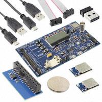
�Please, refer to the latest BLE112 data sheet for information about BLE112 Bluetooth 4.0 single mode
module. The physical outlook, schematics, assembly and the PIN configurations of the interfaces of BLE112
Development Kit are described in this document.
Figure 2: BLE112 Development Kit
1.1 Sensors, display and USB to UART converter
USB to UART converter (U3)
o Manufacturer: Prolific
o Manufacturer part number: PL2303HX rev.D
o Datasheet: http://www.prolific.com.tw/US/ShowProduct.aspx?p_id=156&pcid=41
Display
o Manufacturer: Newhaven Display Intl
o Manufacturer part number: NHD-C0216CZ-FSW-FBW-3V3
o Datasheet: http://www.newhavendisplay.com/specs/NHD-C0216CZ-FSW-FBW-3V3.pdf
Altimeter (U6)
o Manufacturer: Analog Devices
o Manufacturer part number: ADXL350BCEZ-RL
o Datasheet:http://www.analog.com/en/mems-sensors/mems-inertialsensors/adxl350/products/product.html
Bluegiga Technologies Oy
Page 6 of 19
�2 Interfaces
2.1 Powering the Development Board
The board can be powered either from USB or from a coin cell battery. Absolute maximum battery voltage is
3.6V. USB or battery can be chosen with SW1. When using battery, the current measurement should also be
switched off to avoid excessive leakage current to the instrumentation amplifier U2. To minimize the leakage
currents the display, accelerometer and the potentiometer can be turned off and disconnected from the
module by SW2, SW5 and SW6.
2.2 On-Board Debugger
The debugger can be used for SW updates and debugging of the embedded BLE112 module. Using SW14
the debugger output can be routed to the pin header J11 to debug external CC2540 or CC2541 based
devices.
2.2.1 Using the On-Board Debugger to Update the FW of the Embedded BLE112
Module
To update the FW for the embedded BLE112 module, connect USB cable from PC to the USB connector
named “DEBUGGER”. Set the switches as shown in the figure 3. When pressing “RESET DEBUGGER”
button the debugger LED should turn green. Launch BLE Update Tool and follow the instruction in the Profile
Toolkit Developer Guide available in http://www.bluegiga.com/support.
Green = Debugger ready
Red = Debugger not ready
Debugger -> Module
Power -> USB
Figure 3: Using the debugger for the embedded BLE112
2.2.2 Using the On-Board Debugger to Update External Devices
To update the FW for the embedded BLE112 module connect USB cable from PC to the USB connector
named “DEBUGGER”. Set the switches as shown in the figure 4. When pressing “RESET DEBUGGER”
button the debugger LED should turn green.
Bluegiga Technologies Oy
Page 7 of 19
�CC2540 or
CC2541
Based
Device
Green = Debugger ready
Red = Debugger not ready
Debugger -> Output
Power -> USB
Figure 4: Using the debugger for external devices
2.3 Indicator LED
There is a LED connected to the pin P1_0. The LED is powered directly from the battery so the brightness of it
does not depend on if the DCDC is in use or not. However, if the module is not powered but the battery is in
place, i.e. when USB not connected and the power switch is in USB position, there will be leakage through the
LED and the LED is weakly lit. To prevent the LED draining the battery one should make sure either that the
power switch is in BAT position and the module is in deep sleep, or that the battery is not connected when the
power switch is in USB position.
2.4 USB
DKBLE112 operates as USB bus powered device. UART and USB interface share the same USB connector.
To use the USB interface, turn SW13 to USB position.
2.5 UART
UART and USB interface share the same USB connector. To use the USB interface, turn SW13 to UART
position. USB to UART converter creates a virtual COM port for accessing UART interface of the module.
USB to UART converter is Prolific PL2303HX rev.D. Windows driver can be downloaded from Prolific web
site:
(http://www.prolific.com.tw/US/ShowProduct.aspx?p_id=156&pcid=41).
Note: Because the board is using the regulator of the Prolific chip, it will be recognized by the USB as a virtual
COM port even if the power switch is in BAT position. Switching the power switch to BAT position, or
disconnecting the USB converter using SW3, does not turn off the USB top UART converter.
2.6 Display and Accelerometer
The display shares the same SPI interface with the accelerometer. P1_2 is used as the slave select for both.
When P1_2 is low the SPI is used to control the display. Charge pump is generating 3.3V supply for the
display.
Bluegiga Technologies Oy
Page 8 of 19
�2.7 Pin Header and Buttons
All the PIOs are available and permanently connected in the pin header J2. In order to use certain PIOs
through the pin header, that particular PIO must be disconnected from the device to which it is connected so
that it is not actively driven by two devices. Following table shows the PIO connections in the evaluation
board.
PIO Number
Connection In the Development Board
P0_0
P0_1
P0_2
P0_3
P0_4
P0_5
P0_6
PO_7
P1_0
P1_1
P1_2
P1_3
P1_4
P1_5
P1_6
P1_7
P2_0
P2_1
P2_2
Button 1
Button 2
UART CTS
UART RTS
UART TX
UART RX
Trimmer
Accelerometer interrupt
USB pull-up
Display register select
SPI slave select (high=accelerometer, low=display)
SPI CLK
SPI MISO
SPI MOSI
Button 3
DCDC
Button 4
Debugger DD
Debugger DC
Table 1: PIO connections in the development board
2.8 Using the Analog Comparator of BLE112
The analog comparator of BLE112 is fixed to the pins P0_4 (-) and P0_5 (+). The pins overlap with the UART
TX and RX signals in DKBLE112. Thus to use the analog comparator the USB to UART converter must be
turned off. Refer to Bluetooth Smart Software API Reference for details about the analog comparator
configurations.
Bluegiga Technologies Oy
Page 9 of 19
�3 Measuring Current Consumption
The DC current consumption of the whole board can be measured from the headers J3 and J9. The DC
current consumption of the module alone can be measured from the header J5. The peak current
consumption of the module can only be measured when powering the module from USB. When powering from
a battery, the current measurement amplifier should be disconnected with SW12. The peak current
consumption of BLE112 is measured over 3 ohm resistor using an instrumentation amplifier with a gain of 10.
The instrumentation amplifier is powered from USB 5V line and the DC bias is from the 3V3 LDO. Because
the amplifier is powered from the USB VBUS, it can’t be used unless USB is connected. If USB is not
connected then the instrumentation amplifier must be disconnected by SW12 to avoid excessive leakage
current into the input of the amplifier.
+
A=10
3R
-
Ref
3V3
Figure 5: TX current measurement amplifier
To measure the peak TX current consumption of the module, connect a coaxial cable to the BNC connector in
the board and to an oscilloscope. Set the oscilloscope
Coupling: DC
Vertical scale 500 mV/DIV
Horizontal scale: 200 µs/DIV
Level: 2.5 V
Offset: -2.0 V
Trigger: Normal, falling edge
The instrumentation amplifier inverts the signal. The current consumption is calculated by
I
3.3V Vo
30
Bluegiga Technologies Oy
Page 10 of 19
�6
5
4
3
2
1
REVISION RECORD
LTRDATE:
ECO NO:
APPROVED:
4 Schematics And Assembly Drawing
VBAT_REGIN
D
D
R4
2
1
VBAT
NP
Module Current Measurement
L1
U5
HSM G-C1 9 0
R21
SW1
1
AK
4
5
C5
5
2
3
4
5
2
R2
1
C8
J1
BNC_0DEG_PTH
X3
SHORTING_LINK
2V...3V3_MO D
J 5-1
NP
C 32
J 5-2
15pF/50V/C 0G
2
GN D
VOUT
1
NP
C 31
VIN
SW_SLIDE_LSSAM22-V
C
7
AD8228
3
NP
3
U2
1
2
P1
+
0.1uF/10V/X5R
6
Optional LDO
VBUS
3
4
1
2
R1
1
5
3R , 50V, 0.063W, 1%
C 12
4
10uF/6.3V/X5R
C7
10uF/6.3V/X5R
SW12
1
2
0.1uF/10V/X5R
C9
A
D1
HSMG-C1 9 0
1
R 30
2
K
3V3_USB
510R , 50V, 0.063W
C
C3
R 39
VBUS
1uF/16V/X5R
3V3_USB_SW
C6
2
3
8
1
SW_SLIDE_LSSAM22-V
15pF/50V/C 0G
2
0R0, 50V, 2.0A, 0.2W
NP
1
D4
0R 0, 50V, 2.0A, 0.2W
R33
2
510R, 50V, 0.063W
6
+VS
1
2V...3V3_SW
R EF
STAT
6
6
ON/BYP
TPS62730
GN D
5
P1_7/DCDC
2
C 11
SW
VOUT
4
C 10
2.2uF/10V/X5R
2.2µH±20%, 130mA, 0.43ohm
VIN
2.2uF/10V/X5R
3
J 9-2
BATTER YH O LD ER _SMD _C R 2032
1
U4
2
C 14
100uF/16V/10%/TAN
J 12-1
J 12-2
J 9-1
-VS
X1
SHORTING_LINK
Battery curr. meas.
B
B
FID1
1
FIDUCIAL1
FID2
1
FIDUCIAL1
FID3
1
FIDUCIAL1
Figure 6: BLE112 Evaluation Board Schematic (1/6)
COMPANY:
A
Bluegiga Technologies Oy
A
TITLE:
BLE112 Evaluation Board
DRAWN:DATED:
PRA
CHECKED:
2012-09-11
DATED:
-
CODE:
-
QUALITY CONTROL:DATED:
RELEASED:
-C
SIZE:
DRAWING NO:
REV:
-
2.0
DATED:
SCALE:
SHEET:
16
OF
Bluegiga Technologies Oy
Page 11 of 19
�6
5
4
3
2
1
REVISION RECORD
LTRDATE:
ECO NO:
APPROVED:
Push Buttons
D
D
B1
2 B2
3
Header
C1
0.47uF/6.3V/X5R
C2
MOD1
R13
1
P2_2/PROG_DC
P2_1/PROG_DD
P2_0/BUTTON4
P1_7/DCDC
P1_6/BUTTON3
2
27R, 50V, 0.063W, 1%
R14
2
P1_5/SPI_MOSI
GND
AVDD
AVDD
P2_2
P2_1
P2_0
P1_7
P1_6
DVDD_USB
GND
USB+
USBP1_5
J 2-1
P0_1/BUTTON2
J 2-4
J 2-3
P0_2/UART_CTS
J 2-6
J 2-5
P0_3/UART_RTS
J 2-8
J 2-7
P0_4/UART_TX
J 2-10
J 2-9
P0_5/UART_RX
J 2-12
J 2-11
P0_6/TRIMMER
J 2-14
J 2-13
P0_7/ACC_INT1
J 2-16
J 2-15
P1_0/USB_PULL-UP
J 2-18
J 2-17
GND
RESET
P0_0
P0_1
P0_2
P0_3
P0_4
P0_5
P0_6
30
29
28
27
26
25
24
23
22
RESET
P0_0/BUTTON1
P0_1/BUTTON2
P0_2/UART_CTS
P0_3/UART_RTS
P0_4/UART_TX
P0_5/UART_RX
P0_6/TRIMMER
P1_1/LCD_RS
J 2-20
J 2-19
P1_2/CS_LCD/CS_ACC
J 2-22
J 2-21
P1_3/SPI_CLK
J 2-24
J 2-23
P1_4/SPI_MISO
J 2-26
J 2-25
P1_5/SPI_MOSI
J 2-28
J 2-27
P1_6/BUTTON3
J 2-30
J 2-29
P1_7/DCDC
J 2-32
J 2-31
14
15
16
17
18
19
20
21
2V...3V3_SW
C
2V...3V3_MOD
VBAT_REGIN
R 11
200R , 50V, 0.063W
2
R24
D2
100K, 50V, 0.063W
1
2
100K, 50V, 0.063W
P2_1/PROG_DD
P2_2/PROG_DC
2
1
4
3
6
5
HEADER_6PIN_SMD_DUAL
2
3
K
RESET
B
J6
P2_0/BUTTON4
A
R23
1
HSMC-C1 9 0
P1_4/SPI_MISO
P1_3/SPI_C LK
P1_2/C S_LC D /C S_AC C
2
R 34
1
10K, 50V, 0.063W
2
R3
1
1.5K, 50V, 0.063W, +/-5%
27R, 50V, 0.063W, 1%
2V...3V3_MOD
J 2-2
BLE112-A
P1_4
P1_3
P1_2
P1_1
P1_0
P0:7
D VD D
GN D
1
USB-
1
2
3
4
5
6
7
8
9
10
11
12
13
P0_7/AC C _IN T1
USB+
B
P0_0/BUTTON1
2V...3V3_MOD
P2_0/BU TTO N 4
P1_6/BU TTO N 3
R 20
A1
A2 1
510R , 50V, 0.063W 4
SW11
R 10
A1
A2 1
510R , 50V, 0.063W 4
R 27
A1
A2 1
510R , 50V, 0.063W 4
SW10
0.47uF/6.3V/X5R
SW8
P0_1/BU TTO N 2
C
P0_0/BU TTO N 1
R 26
A1
A2 1
510R , 50V, 0.063W
4
SW9
B1
2 B2
3
B1
2 B2
3
B1
2 B2
3
2V...3V3_SW
P1_1/LC D _R S
P1_0/U SB_PU LL-U P
1
4
SW4
Figure 7: BLE112 Evaluation Board Schematic (2/6)
A
COMPANY:
Bluegiga Technologies Oy
A
TITLE:
BLE112 Evaluation Board
DRAWN:DATED:
PRA
CHECKED:
2012-09-11
DATED:
-
CODE:
-
QUALITY CONTROL:DATED:
RELEASED:
SIZE:
DRAWING NO:
REV:
-C-
2.0
DATED:
SCALE:
SHEET:
26
OF
Bluegiga Technologies Oy
Page 12 of 19
�6
5
4
3
2
1
REVISION RECORD
Disconnet USB To UART Converter
LTRDATE:
ECO NO:
APPROVED:
2V...3V3_SW
2
P0_4/UART_TX
D
6
P0_4/UART_TX_PL
3
P0_3/UART_RTS_PL
6
P0_5/UART_RX
3
P0_2/UART_CTS
1
5
P0_3/UART_RTS
D
48
7
U16
74AUP2G126
2V...3V3_SW
SW3
4
5
6
2V...3V3_SW
1
2
3
SW_SLIDE_LSSAM22-V
2
P0_5/UART_RX_PL
1
5
P0_2/UART_CTS_PL
48
7
U17
74AUP2G126
C
C
USB To UART Converter
1
USB curr. meas.
J 3-1
C 41
VBUS
L4
J 3-2
C 20
FB 1k ohm
X2
SHORTING_LINK
20VDD_5
LDO 3v 3
J4
6
2
5
3
4
5
1
6
USB-
U32
USBLC6-2
2
33R, 50V, 0.063W, +/-5%
1
1
3
USB+
2
RTS
CTS
3
11
DTR
DSR
RI
DCD
2
9
6
10
P0_2/UART_CTS_PL
P0_3/UART_RTS_PL
EE_CLK 13
EE_DATA 14
33R, 50V, 0.063W, +/-5%
SW_SLIDE_LSSAM22-V
SHTD
26
P0_5/UART_RX_PL
P0_4/UART_TX_PL
B
22
23 GP0
GP1
R16
2
4
PLL_TEST
25
GN D _A
27
OSC1
28 OSC2
NC
NC
NC
U3
12
8
19
24
R25
1
2
5.1K, 50V, 0.063W
GN D
21
GN D
7
GN D
18
G I D D +D -5 V
1
R17
3V3_USB_SW
17
TXD 1
RXD 5
15D+
16 D-
SW13
4
VO_33
VDD_325
USB to UART
B
C4
D3
0.1 u F/ 1 0 V/ X5 R
R 22
2
R15
2.2 u F/ 1 0 V/ X5 R
0R0, 50V, 2.0A, 0.2W
2
1
2.2 u F/ 1 0 V/ X5 R
3V3_USB
1 . 5 K, 5 0 V, 0 .0 6 3 W
D6
VBUS_DEBUG
PL2303HX
Figure 8: BLE112 Development Board Schematic (3/6)
A
COMPANY:
Bluegiga Technologies Oy
A
TITLE:
BLE112 Evaluation Board
DRAWN:DATED:
PRA
CHECKED:
2012-09-11
DATED:
-
CODE:
-
QUALITY CONTROL:DATED:
Bluegiga Technologies Oy
RELEASED:
SIZE:
DRAWING NO:
REV:
-C-2.0
DATED:
SCALE:
SHEET:
36
OF
Page 13 of 19
�6
5
4
3
2
1
REVI SI ON RECORD
LTRDATE:
ECO NO:
APPROVED:
VDD_ DI SPLAY
C 22
C 21
0.47uF/6.3V/X5R
D
0.47uF/6.3V/X5R
C 28
2
R 28
2 V. . . 3 V3 _SW
Display
VDD_DISPL AY
3
1
10R , 50V, 0.063W
VDD_ DISPL AY
If VDD_DISPLAY floats in voltage range
that is not spec ified for U15, there will be
exc es s ive c urrent leakage in U15.
T o avoid excess ive leakage while shutting
down the dis play U15 is us ed to pull
pull VDD_DISPLAY to known state (GND)
0.47uF/6.3V/X5R
D
D
2
1
R 12
2
S
3 V3_ USB_ SW
U1 0
DISPL AY-NHD-C021 6 CZ-FSW-FBW-3 V3
U1 5
7 4 AVC4 T24 5
C
NP
C 17
1
NP
R 19
SW7
R ST
RS
C SB
SC L
SI
VSS
VD D
VO U T
C 1+
C 1LED +
LED -
VCCB
1 OE
2 OE
1 B1
1 B2
2 B1
2 B2
GND
2
3
VCCA
1DI R
2DI R
1A1
1A2
2A1
2A2
GND
1
2
3
4
5
6
7
8
9
10
11
12
P1 _ 1/LCD_ RS
P1_3 / SPI _ CL K
P1 _ 5 / SPI_M OSI
P1 _ 2 / CS_ L CD/ CS_ ACC
16
15
14
13
12
11
10
9
1
4
1
2
3
4
5
6
7
8
2
G
10K, 50V, 0.063W
U1 3
1
C
C 29
1uF/16V/X5R
C30
2 .2 u F/ 1 0V/X5 R
NP
2
1
R1 8
2
2
L5
NP
1
R8
1
R7
SW_ SLIDE_ L SSAM 2 2-V
Disconnect And Shut Down Display
C2 -
C 25
10
6
8
1uF/16V/X5R
C2+
C 27
C1 +
5
1uF/16V/X5R
LBO
2 GN D
1R, 1 2 5 mW, 5 %
3
OUT
L BI
3
C1 9
SNOOZE
2
1
4
IN
0R 0, 50V, 2.0A, 0.2W
1
5
6
1uF/16V/X5R
NP
4
1
C 26
R5
2
1
R6
0R 0, 50V, 2.0A, 0.2W
C 39
10uF/6.3V/X5R
SW5
B
1uF/16V/X5R
C 23
C 16
2 V...3 V3 _ SW
10uF/6.3V/X5R
2
U8
TPS6 021 3 DGS
7
B
Charge pump to generate 3V3 supply
for the display
Figure 9: BLE112 Development Board Schematic (4/6)
COMPANY:
A
Bluegiga Technologies Oy
A
TI TL E:
BLE112 Evaluation Board
DRAWN: DATED:
PRA
CHECKED:
2012- 09- 11
DATED:
-
CODE:
-
QUALITY CONTROL : DATED:
RELEASED:
SIZE:
DRAWING NO:
REV:
-C-2.0
DATED:
SCAL E:
SHEET:
56
OF
Bluegiga Technologies Oy
Page 14 of 19
�6
5
4
3
2
1
REVISION RECORD
LTRDATE:
Accelerometer
ECO NO:
APPROVED:
2V...3V3_SW
48
SW_ACC_EN
U7
74AUP2G126
P1_2/CS_LCD/CS_ACC
C 34
2
U12
74AUP1G04GW
0.1uF/10V/X5R /10%
4
7
35
5
C 33
P1_3/SPI_CLK
1
0.1uF/10V/X5R /10%
2
3
C 15
6
D
2V...3V3_SW
0.1uF/10V/X5R /10%
2V...3V3_SW
D
2V...3V3_SW
Connect / Disconnect
SW2
4
5
2V...3V3_SW
6
1
2
SW_ACC_EN
3
SW_SLIDE_LSSAM22-V
2
6
P0_7/ACC_INT1
6
SD I
7
SD O
8
CS
1
VDD
2
NC
3 NC
4
5 SCLK
NC
C
16
GND
15
NC
14
VD D
3
7
J 10-1
5
U9
74AUP2G126
48
C 13
0.1uF/10V/X5R /10%
1
13
GND
12
GND
INT1 11
10
NC 9
INT2
C
2V...3V3_SW
U6
ADXL350
2
6
P1_4/SPI_MISO
1
2V...3V3_SW
5
P1_5/SPI_MOSI
3
48
7
5
U11
74AUP2G126
U14
VCC
A 1
4 Y
2
B
GND
3
NC7SZ32
B
B
Connect / Disconnect
3
2V...3V3_SW
3
+
4 -
U1
OPAMP_ISL28194
1
5
2
4
5
6
COMPANY:
Bluegiga Technologies Oy
1
2
2
R9
6
SW6
1
PO TEN TIOMETER _1MOH M
C 19
A
0.47uF/6.3V/X5R
Potentiometer
A
P0_6/TRIMMER
3
TITLE:
SW_SLIDE_LSSAM22-V
BLE112 Evaluation Board
DRAWN:DATED:
PRA
CHECKED:
2012-09-11
DATED:
CODE:
-QUALITY CONTROL:DATED:
Figure 10: BLE112 Development Board Schematic (5/6)
RELEASED:
-
SIZE:
DRAWING NO:
REV:
C-
2.0
DATED:
SCALE:
SHEET:
46
OF
Bluegiga Technologies Oy
Page 15 of 19
�6
5
4
3
2
1
REVISI ON RECORD
3V3_USB_SW
5
1
DEBUG_SW
4
U24
2V...3V3_SW
2
D
74 AHC1G0 8
2
1
DEBUG_SW
2V. .. 3V3_ SW
4
2
3V3 _USB_ SW
6
3
VD D
U 29-B
SW1 4
5
1
VDD_TARGET
3
3
NO 6
5
D
U3 1
1
NC 4
LED_ RED
G
3 V3_USB_SW
SW19
SW_TS5A4624
2
1
16
15
14
13
12
11
10
9
NO 6
P2_1 /PROG_DD
NC 4
EXT_ DD
5
C 37
1uF/6.3V/X5R
2V...3V3_SW
VD D
3 V3 _USB_ SW
2
3 V3_USB_SW
2
1
GN D
3
1
B
2
1
NO 6
RESET
NC 4
EXT_ RESET
C2 4
3 3 pF/50V/C0G
5
D
U2 8
DBG_ RESET
1
G
S
2
27R, 5 0 V, 0. 0 6 3W
3
R36
EXT_DC
SW1 6
SW_TS5A4 624
GN D
2
27R, 5 0 V, 0. 0 6 3W
NC 4
3
R37
1
R 40
13
CC2511
P2_2/PROG_ DC
2V. . .3V3_ SW
Y1
XTAL_ 4 8MHZ_ 5X3.2MM
U2 2
C C 2511_D D
C C 2511_D C
LED _R ED
LED _G R EEN
2
1
R 38
B
2
2
4
U36
USBLC6 -2
R3 2
1
56K, 5 0V, 0 . 0 63W
10
11
12
13
14
15
16
17
18
G
3
27
26
25
24
23
22
21
20
19
4
5
RBI AS
AVDD
AVDD
RF_ N
RF_ P
AVDD
XOSC_ Q1
XOSC_ Q2
AVDD
2
6
2
1.5K, 50V, 0.063W
ID D +
DBG_RESET
1
P1 _2
DVDD2
P1 _1
P1 _0
P0 _0
P0 _1
P0 _2
P0 _3
P0 _4
C 18
33pF/50V/C 0G
D - 5V
J8
DBG_DC
4.7K, 50V, 0.063W
1
2
3
4
5
6
7
8
9
DBG_ DC_DI R
NO 6
5
DP
DM
D VD D
P0_5
P2_0
P2_1
P2_2
P2_3
P2_4
VBUS_DEBUG
40
GN D
39
GN D
G N D 38
37
GN D
36
P1_3
35
P1_4 34
P1_5
33
P1_6
32
P1_7
31
R ESET
30
D C O U PL
29
AVD D _D R EG 28
G U AR D
1
VD D
D BG _D D _D IR
D BG _D D
C C 2511_R ESET
A1
A2 1
4
SW17
C
SW15
SW_TS5A4624
3
B1
2 B2
3
VCCB
1OE
2OE
1B1
1B2
2B1
2B2
GND
GN D
DBG_ DC
VCCA
1 DI R
2 DI R
1 A1
1 A2
2 A1
2 A2
GND
VD D
2
4.7K, 50V, 0.063W
R 29
R 31
1
2
R 41
1
1
2
3
4
5
6
7
8
DBG_DD_DIR
DBG_DC_DIR
DBG_ DD
CC2 511_ RESET
C
2V. .. 3V3_ SW
U23
74AVC4T24 5
4.7K, 50V, 0.063W
2
1
3V3 _USB_ SW
4.7K, 50V, 0.063W
3
2
S
2
S
GN D
U3 0
1
G
APPROVED:
3
1
R 43
2
150R , 50V, 0.063W
MOD DEBUG / EXT DEBUG
SW_SL I DE_LSSAM22-V
D
LED_GREEN
ECO NO:
2V... 3 V3_SW
LED _LTST-C 155G EKT
2
R 42
1
U 29-A
D
LED _LTST-C 155G EKT 150R , 50V, 0.063W
LTRDATE:
SW1 8
SW_TS5 A462 4
3V3 _ USB_ SW
VDD_TARGET
J7
CC2 511_ DC
A
CC2 5 11_RESET
1
R44
2
1 0 0R, 5 0 V, 0. 0 6 3W
R47
2
1
1 0 0R, 5 0 V, 0. 0 6 3W
J 11
1
2
3
4
5
6
1
R4 6
2
CC2511 _ DD
EXT_DC
1 00R, 50V, 0 . 0 63W
78
HEADER_2 X5_SMD_2 . 54MM
2
3
4
5
6
COMPANY:
Bluegiga Technologies Oy
EXT_DD
78
EXT_RESET
910
1
9 10
2 V...3V3_SW
HEADER_ 2X5_ SMD_1.27MM
CC2511 PROGRAMMING INTERFACEPROGRAMMING INTERFACE
A
TI TLE:
BLE112 Evaluation Board
DRAWN:DATED:
PRA
CHECKED:
2012-09-11
DATED:
-
CODE:
-
QUALITY CONTROL:DATED:
DRAWI NG NO:
REV:
-C-2.0
Figure 11: BLE112 Development Board Schematic (6/6)
RELEASED:
SIZE:
DATED:
SCALE:
SHEET:
66
OF
Bluegiga Technologies Oy
Page 16 of 19
�Figure 12: BLE112 Development Board Assembly Drawing
Bluegiga Technologies Oy
Page 17 of 19
�5 WEEE Compliance
The crossed-out wheeled bin means that within the European Union the product
must be taken to separate collection at the product end-of-life. Do not dispose of
these products as unsorted municipal waste.
Bluegiga Technologies Oy
Page 18 of 19
�6 Contact Information
Sales:
sales@bluegiga.com
Technical support:
support@bluegiga.com
http://techforum.bluegiga.com
Orders:
orders@bluegiga.com
WWW:
www.bluegiga.com
www.bluegiga.hk
Head Office / Finland:
Phone: +358-9-4355 060
Fax: +358-9-4355 0660
Sinikalliontie 5A
02630 ESPOO
FINLAND
Postal address / Finland:
P.O. BOX 120
02631 ESPOO
FINLAND
Sales Office / USA:
Phone: +1 770 291 2181
Fax: +1 770 291 2183
Bluegiga Technologies, Inc.
3235 Satellite Boulevard, Building 400, Suite 300
Duluth, GA, 30096, USA
Sales Office / Hong-Kong:
Phone: +852 3972 2186
Bluegiga Technologies Ltd.
Unit 10-18
32/F, Tower 1, Millennium City 1
388 Kwun Tong Road
Kwun Tong, Kowloon
Hong Kong
Bluegiga Technologies Oy
Page 19 of 19
�