EZR32WG Wireless MCUs
EZR32WG330 Data Sheet
EZR32WG330 Wireless MCU family with ARM Cortex-M4 CPU,
USB, and sub-GHz Radio
The EZR32WG Wireless MCUs are the latest in Silicon Labs family of wireless MCUs
delivering a high-performance, low-energy wireless solution integrated into a small form
factor package. By combining a high-performance sub-GHz RF transceiver with an energy efficient 32-bit MCU, the EZR32WG family provides designers the ultimate in flexibility with a family of pin-compatible devices that scale with 64/128/256 kB of flash and support Silicon Labs EZRadio or EZRadioPRO transceivers. The ultra-low power operating
modes and fast wake-up times of the Silicon Labs energy friendly 32-bit MCUs, combined with the low transmit and receive power consumption of the sub-GHz radio, result
in a solution optimized for battery powered applications.
32-Bit ARM Cortex wireless MCUs applications include the following:
• Energy, gas, water, and smart metering
• Health and fitness applications
• Consumer electronics
• Alarm and security systems
• Building and home automation
KEY FEATURES
• Silicon Labs’ first 32-bit Wireless MCUs
• Based on ARM Cortex M3 (LG) and M4
(WG) CPU cores with 256 kB of flash and
32 kB RAM
• Best-in-class RF performance with EZradio
and EZRadioPro transceivers
• Ultra-low power wireless MCU
• Low transmit and receive currents
• Ultra-low power standby and sleep
modes
• Fast wake-up time
• Low energy sensor interface (LESENSE)
• Rich set of peripherals including 12-bit
ADC and DAC, multiple communication
interfaces (USB, UART, SPI, I2C), multiple
GPIO and timers
• AES accelerator with 128/256-bit keys
silabs.com | Building a more connected world.
Rev. 2.0
�EZR32WG330 Data Sheet
Feature List
1. Feature List
The WG highlighted features are listed below.
MCU Features
• ARM Cortex-M4 CPU platform
• Up to 48 MHz
• 64/128/256 kB Flash with 32 kB RAM
• Hardware AES with 128/256-bit keys
• Flexible Energy Management System
• 20 nA @ 3 V Shutoff Mode
• 0.65 µA @ 3 V Stop Mode
• 225 µA/MHz @ 3 V Run Mode
• Timers/Counters
• 4× Timer/Counter
• 4×3 Compare/Capture/PWM channels
• Low Energy Timer
• Real-Time Counter
• 16/8-bit Pulse Counter
• Watchdog Timer
• Communication interfaces
• 2× USART (UART/SPI)
• 2× UART
• 2× Low Energy UART
• 2× I2C Interface with SMBus support
• Universal Serial Bus (USB)
• Ultra low power precision analog peripherals
• 12-bit 1 Msamples/s ADC
• On-chip temperature sensor
• 12-bit 500 ksamples/s DAC
• 2× Analog Comparator
• 2x Operational Amplifier
• Low Energy Sensor Interface (LESENSE)
• Up to 38 General Purpose I/O pins
silabs.com | Building a more connected world.
RF Features
• Frequency Range
• 142-1050 MHz
• Modulation
• (G)FSK, 4(G)FSK, (G)MSK, OOK
• Receive sensitivity up to -133 dBm
• Up to +20 dBm max output power
• Low active power consumption
• 10/13 mA RX
• 18 mA TX at +10 dBm
• 6 mA @ 1.2 kbps (Preamble Sense)
• Data rate = 100 bps to 1 Mbps
• Excellent selectivity performance
• 69 dB adjacent channel
• 79 dB blocking at 1 MHz
• Antenna diversity and T/R switch control
• Highly configurable packet handler
• TX and RX 64 byte FIFOs
• Automatic frequency control (AFC)
• Automatic gain control (AGC)
• IEEE 802.15.4g compliant
System Features
•
•
•
•
•
Power-on Reset and Brown-Out Detector
Debug Interface
Temperature range -40 to 85 °C
Single power supply 1.98 to 3.8 V
QFN64 package
Rev. 2.0 | 2
�EZR32WG330 Data Sheet
Ordering Information
2. Ordering Information
The table below shows the available EZR32WG330 devices.
Table 2.1. Ordering Information
Radio
Flash (kB)
RAM (kB)
Power Amplifier
(dBm)
Max Sensitivity (dBm)
Supply
Voltage (V)
Package
EZR32WG330FxxxR55G-C0
EZRadio
64-256
32
+13
-116
1.98 - 3.8
QFN64
EZR32WG330FxxxR60G-C0
EZRadioPro
64-256
32
+13
-129
1.98 - 3.8
QFN64
EZR32WG330FxxxR61G-C0
EZRadioPro
64-256
32
+16
-129
1.98 - 3.8
QFN64
EZR32WG330FxxxR63G-C0
EZRadioPro
64-256
32
+20
-129
1.98 - 3.8
QFN64
EZR32WG330FxxxR67G-C0
EZRadioPro
64-256
32
+13
-133
1.98 - 3.8
QFN64
EZR32WG330FxxxR68G-C0
EZRadioPro
64-256
32
+20
-133
1.98 - 3.8
QFN64
EZR32WG330FxxxR69G-C0
EZRadioPro
64-256
32
+13 & 20
-133
1.98 - 3.8
QFN64
Ordering
Table 2.2. Flash Sizes
Example Part Number
Flash Size
EZR32WG330F64R55G-C0
64 kB
EZR32WG330F128R55G-C0
128 kB
EZR32WG330F256R55G-C0
256 kB
Note: Add an "(R)" at the end of the device part number to denote tape and reel option.
Visit www.silabs.com for information on global distributors and representatives.
silabs.com | Building a more connected world.
Rev. 2.0 | 3
�Table of Contents
1. Feature List . . . . . . . . . . . . . . . . . . . . . . . . . . . . . . . . 2
2. Ordering Information . . . . . . . . . . . . . . . . . . . . . . . . . . . . 3
3. System Overview . . . . . . . . . . . . . . . . . . . . . . . . . . . . . . 7
3.1 Introduction . . . . . . . . . . . . . . . . . . . . . .
3.1.1 ARM Cortex-M4 Core . . . . . . . . . . . . . . . . .
3.1.2 Debugging . . . . . . . . . . . . . . . . . . . . .
3.1.3 Memory System Controller (MSC) . . . . . . . . . . . . .
3.1.4 Direct Memory Access Controller (DMA) . . . . . . . . . . .
3.1.5 Reset Management Unit (RMU) . . . . . . . . . . . . . .
3.1.6 Energy Management Unit (EMU) . . . . . . . . . . . . .
3.1.7 Clock Management Unit (CMU) . . . . . . . . . . . . . .
3.1.8 Watchdog (WDOG) . . . . . . . . . . . . . . . . . .
3.1.9 Peripheral Reflex System (PRS) . . . . . . . . . . . . .
3.1.10 Universal Serial Bus Controller (USB) . . . . . . . . . . .
3.1.11 Inter-Integrated Circuit Interface (I2C) . . . . . . . . . . .
3.1.12 Universal Synchronous/Asynchronous Receiver/Transmitter (USART)
3.1.13 Pre-Programmed UART Bootloader . . . . . . . . . . . .
3.1.14 Universal Asynchronous Receiver/Transmitter (UART) . . . . .
3.1.15 Low Energy Universal Asynchronous Receiver/Transmitter (LEUART)
3.1.16 Timer/Counter (TIMER) . . . . . . . . . . . . . . . .
3.1.17 Real Time Counter (RTC) . . . . . . . . . . . . . . .
3.1.18 Backup Real Time Counter (BURTC) . . . . . . . . . . .
3.1.19 Low Energy Timer (LETIMER) . . . . . . . . . . . . . .
3.1.20 Pulse Counter (PCNT) . . . . . . . . . . . . . . . .
3.1.21 Analog Comparator (ACMP) . . . . . . . . . . . . . .
3.1.22 Voltage Comparator (VCMP) . . . . . . . . . . . . . .
3.1.23 Analog to Digital Converter (ADC) . . . . . . . . . . . .
3.1.24 Digital to Analog Converter (DAC) . . . . . . . . . . . .
3.1.25 Operational Amplifier (OPAMP) . . . . . . . . . . . . .
3.1.26 Low Energy Sensor Interface (LESENSE) . . . . . . . . . .
3.1.27 Backup Power Domain . . . . . . . . . . . . . . . .
3.1.28 Advanced Encryption Standard Accelerator (AES) . . . . . . .
3.1.29 General Purpose Input/Output (GPIO) . . . . . . . . . . .
3.1.30 EZRadio® and EZRadioPro® Transceivers. . . . . . . . . .
.
.
.
.
.
.
.
.
.
.
.
.
.
.
.
.
.
.
.
.
.
.
.
.
.
.
.
.
.
.
.
.
.
.
.
.
.
.
.
.
.
.
.
.
.
.
.
.
.
.
.
.
.
.
.
.
.
.
.
.
.
.
.
.
.
.
.
.
.
.
.
.
.
.
.
.
.
.
.
.
.
.
.
.
.
.
.
.
.
.
.
.
.
.
.
.
.
.
.
.
.
.
.
.
.
.
.
.
.
.
.
.
.
.
.
.
.
.
.
.
.
.
.
.
.
.
.
.
.
.
.
.
.
.
.
.
.
.
.
.
.
.
.
.
.
.
.
.
.
.
.
.
.
.
.
.
.
.
.
.
.
.
.
.
.
.
.
.
.
.
.
.
.
.
.
.
.
.
.
.
.
.
.
.
.
.
.
.
.
.
.
.
.
.
.
.
.
.
.
.
.
.
.
.
.
.
.
.
.
.
.
.
.
.
.
.
.
.
.
.
.
.
.
.
.
.
.
.
.
.
.
.
.
.
.
.
.
.
.
.
.
.
.
.
.
.
.
.
. 7
. 7
. 7
. 7
. 8
. 8
. 8
. 8
. 8
. 8
. 8
. 8
. 8
. 8
. 9
. 9
. 9
. 9
. 9
. 9
. 9
. 9
. 9
. 9
.10
.10
.10
.10
.10
.10
.11
3.2 Configuration Summary .
.
.
.
.
.
.
.
.
.
.
.
.
.
.
.
.
.
.
.
.
.
.
.
.
.
.13
3.3 Memory Map
.
.
.
.
.
.
.
.
.
.
.
.
.
.
.
.
.
.
.
.
.
.
.
.
.
.14
.
.
.
.
4. Electrical Specifications
. . . . . . . . . . . . . . . . . . . . . . . . . . 15
4.1 Test Conditions . . . . . . . .
4.1.1 Typical Values . . . . . .
4.1.2 Minimum and Maximum Values .
.
.
.
.
.
.
.
.
.
.
.
.
.
.
.
.
.
.
.
.
.
.
.
.
.
.
.
.
.
.
.
.
.
.
.
.
.
.
.
.
.
.
.
.
.
.
.
.
.
.
.
.
.
.
.
.
.
.
.
.
.
.
.
.15
.15
.15
4.2 Absolute Maximum Ratings.
.
.
.
.
.
.
.
.
.
.
.
.
.
.
.
.
.
.
.
.
.
.
.
.
.15
4.3 Thermal Characteristics .
.
.
.
.
.
.
.
.
.
.
.
.
.
.
.
.
.
.
.
.
.
.
.
.
.16
silabs.com | Building a more connected world.
.
Rev. 2.0 | 4
�4.4 General Operating Conditions .
.
.
.
.
.
.
.
.
.
.
.
.
.
.
.
.
.
.
.
.
.
.
.
.16
4.5 Current Consumption .
.
.
.
.
.
.
.
.
.
.
.
.
.
.
.
.
.
.
.
.
.
.
.
.17
4.6 Transitions between Energy Modes .
.
.
.
.
.
.
.
.
.
.
.
.
.
.
.
.
.
.
.
.
.
.19
4.7 Power Management .
.
.
.
.
.
.
.
.
.
.
.
.
.
.
.
.
.
.
.
.
.
.
.
.
.
.
.19
4.8 Flash .
.
.
.
.
.
.
.
.
.
.
.
.
.
.
.
.
.
.
.
.
.
.
.
.
.
.
.20
4.9 General Purpose Input Output .
.
.
.
.
.
.
.
.
.
.
.
.
.
.
.
.
.
.
.
.
.
.
.
.21
4.10 Oscillators . .
4.10.1 LFXO . .
4.10.2 HFXO . .
4.10.3 LFRCO .
4.10.4 HFRCO .
4.10.5 AUXHFRCO
4.10.6 ULFRCO .
.
.
.
.
.
.
.
.
.
.
.
.
.
.
.
.
.
.
.
.
.
.
.
.
.
.
.
.
.
.
.
.
.
.
.
.
.
.
.
.
.
.
.
.
.
.
.
.
.
.
.
.
.
.
.
.
.
.
.
.
.
.
.
.
.
.
.
.
.
.
.
.
.
.
.
.
.
.
.
.
.
.
.
.
.
.
.
.
.
.
.
.
.
.
.
.
.
.
.
.
.
.
.
.
.
.
.
.
.
.
.
.
.
.
.
.
.
.
.
.
.
.
.
.
.
.
.
.
.
.
.
.
.
.
.
.
.
.
.
.
.
.
.
.
.
.
.
.
.
.
.
.
.
.
.
.
.
.
.
.
.
.29
.29
.30
.31
.32
.36
.36
4.11 Analog Digital Converter (ADC) .
4.11.1 Typical Performance . . .
.
.
.
.
.
.
.
.
.
.
.
.
.
.
.
.
.
.
.
.
.
.
.
.
.
.
.
.
.
.
.
.
.
.
.
.
.
.
.
.
.
.
.
.
.37
.44
4.12 Digital Analog Converter (DAC) .
.
.
.
.
.
.
.
.
.
.
.
.
.
.
.
.
.
.
.
.
.
.
.50
4.13 Operational Amplifier (OPAMP) .
.
.
.
.
.
.
.
.
.
.
.
.
.
.
.
.
.
.
.
.
.
.
.52
4.14 Analog Comparator (ACMP) .
.
.
.
.
.
.
.
.
.
.
.
.
.
.
.
.
.
.
.
.
.
.
.
.56
4.15 Voltage Comparator (VCMP) .
.
.
.
.
.
.
.
.
.
.
.
.
.
.
.
.
.
.
.
.
.
.
.
.58
4.16 I2C
.
.
.
.
.
.
.
.
.
.
.
.
.
.
.
.
.
.
.
.
.
.
.
.59
4.17 Radio. . . . . . . . . . . . . . . . . . . . .
4.17.1 EZRadioPRO (R6x) DC Electrical Characteristics . . . .
4.17.2 EZRadioPRO (R6x) Synthesizer AC Electrical Characteristics
4.17.3 EZRadioPRO (R6x) Receiver AC Electrical Characteristics .
4.17.4 EZRadioPRO (R6x) Transmitter AC Electrical Characteristics
4.17.5 EZRadioPRO (R6x) Radio Auxillary Block Specifications . .
4.17.6 EZRadio (R55) DC Electrical Characteristics . . . . . .
4.17.7 EZRadio (R55) Synthesizer AC Electrical Characteristics . .
4.17.8 EZRadio (R55) Receiver AC Electrical Characteristics . . .
4.17.9 EZRadio (R55) Transmitter AC Electrical Characteristics . .
4.17.10 EZRadio (R55) Radio Auxiliary Block Specifications . . .
4.17.11 Radio Digital I/O Specification . . . . . . . . . .
.
.
.
.
.
.
.
.
.
.
.
.
.
.
.
.
.
.
.
.
.
.
.
.
.
.
.
.
.
.
.
.
.
.
.
.
.
.
.
.
.
.
.
.
.
.
.
.
.
.
.
.
.
.
.
.
.
.
.
.
.
.
.
.
.
.
.
.
.
.
.
.
.
.
.
.
.
.
.
.
.
.
.
.
.
.
.
.
.
.
.
.
.
.
.
.
.
.
.
.
.
.
.
.
.
.
.
.
.
.
.
.
.
.
.
.
.
.
.
.
.
.
.
.
.
.
.
.
.
.
.
.
.60
.61
.62
.63
.66
.67
.68
.68
.69
.70
.71
.72
4.18 Digital Peripherals .
.
.
.
.
.
.
.
.
.
.
.
.73
.
.
.
.
.
.
.
.
.
.
.
.
.
.
.
.
.
.
.
.
.
.
.
.
.
.
.
.
.
.
.
.
.
.
.
.
.
.
.
.
.
.
.
.
.
.
.
.
.
.
.
.
.
.
.
.
.
.
.
.
.
.
.
.
.
.
.
5. Pinout and Package . . . . . . . . . . . . . . . . . . . . . . . . . . . . 74
5.1 Pinout .
.
.
.
.
.
.
.
.
.
.
.
.
.
.
.
.
.
.
.
.
.
.
.
.
.
.
.
.
.
.
.
.74
5.2 Pin Descriptions
.
.
.
.
.
.
.
.
.
.
.
.
.
.
.
.
.
.
.
.
.
.
.
.
.
.
.
.
.75
5.3 Alternate Functionality Pinout .
.
.
.
.
.
.
.
.
.
.
.
.
.
.
.
.
.
.
.
.
.
.
.
.78
5.4 GPIO Pinout Overview .
.
.
.
.
.
.
.
.
.
.
.
.
.
.
.
.
.
.
.
.
.
.
.
.
.
.82
5.5 Opamp Pinout Overview .
.
.
.
.
.
.
.
.
.
.
.
.
.
.
.
.
.
.
.
.
.
.
.
.
.
.82
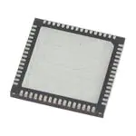
5.6 QFN64 Package .
.
.
.
.
.
.
.
.
.
.
.
.
.
.
.
.
.
.
.
.
.
.
.
.
.
.83
.
.
6. PCB Layout and Soldering
silabs.com | Building a more connected world.
. . . . . . . . . . . . . . . . . . . . . . . . . 84
Rev. 2.0 | 5
�6.1 Recommended PCB Layout
.
.
.
.
.
.
.
.
.
.
.
.
.
.
.
.
.
.
.
.
.
.
.
.
.84
6.2 Soldering Information .
.
.
.
.
.
.
.
.
.
.
.
.
.
.
.
.
.
.
.
.
.
.
.
.
.85
7. Top Marking . . . . . . . . . . . . . . . . . . . . . . . . . . . . . . .
86
8. Revision History
8.1 Revision History
.
.
. . . . . . . . . . . . . . . . . . . . . . . . . . . . . 87
.
.
.
silabs.com | Building a more connected world.
.
.
.
.
.
.
.
.
.
.
.
.
.
.
.
.
.
.
.
.
.
.
.
.
.
.87
Rev. 2.0 | 6
�EZR32WG330 Data Sheet
System Overview
3. System Overview
3.1 Introduction
The EZR32WG330 Wireless MCUs are the latest in the Silicon Labs family of wireless MCUs delivering a high-performance, low-energy wireless solution integrated into a small form factor package. By combining a high performance sub-GHz RF transceiver with an
energy efficient 32-bit ARM Cortex-M4, the EZR32WG family provides designers with the ultimate in flexibility with a family of pin-compatible parts that scale from 64 to 256 kB of flash and support Silicon Labs EZRadio or EZRadioPRO transceivers. The ultra-low power
operating modes and fast wake-up times combined with the low transmit and receive power consumption of the sub-GHz radio result in
a solution optimized for low power and battery powered applications. For a complete feature set and in-depth information on the modules, refer to the EZR32WG Reference Manual.
The EZR32WG330 block diagram is shown below.
Figure 3.1. Block Diagram
3.1.1 ARM Cortex-M4 Core
The ARM Cortex-M4 includes a 32-bit RISC processor which can achieve as much as 1.25 Dhrystone MIPS/MHz. A Memory Protection
Unit with support for up to 8 memory segments is included, as well as a Wake-up Interrupt Controller handling interrupts triggered while
the CPU is asleep. The EZR32 implementation of the Cortex-M4 is described in detail in the EZR32 Cortex-M4 Reference Manual.
3.1.2 Debugging
These devices include hardware debug support through a 2-pin serial-wire debug interface and an Embedded Trace Module (ETM) for
data/instruction tracing. In addition there is also a 1-wire Serial Wire Viewer pin which can be used to output profiling information, data
trace and software-generated messages.
3.1.3 Memory System Controller (MSC)
The Memory System Controller (MSC) is the program memory unit of the EZR32WG microcontroller. The flash memory is readable and
writable from both the Cortex-M4 and DMA. The flash memory is divided into two blocks: the main block and the information block.
Program code is normally written to the main block. Additionally, the information block is available for special user data and flash lock
bits. There is also a read-only page in the information block containing system and device calibration data. Read and write operations
are supported in the energy modes EM0 and EM1.
silabs.com | Building a more connected world.
Rev. 2.0 | 7
�EZR32WG330 Data Sheet
System Overview
3.1.4 Direct Memory Access Controller (DMA)
The Direct Memory Access (DMA) controller performs memory operations independently of the CPU. This has the benefit of reducing
the energy consumption and the workload of the CPU, and enables the system to stay in low energy modes when moving, for instance,
data from the USART to RAM or from the External Bus Interface to a PWM-generating timer. The DMA controller uses the PL230
µDMA controller licensed from ARM.
3.1.5 Reset Management Unit (RMU)
The Reset Management Unit (RMU) is responsible for handling the reset functionality of the EZR32WG.
3.1.6 Energy Management Unit (EMU)
The Energy Management Unit (EMU) manages all the low energy modes (EM) in EZR32WG microcontrollers. Each energy mode manages if the CPU and the various peripherals are available. The EMU can also be used to turn off the power to unused SRAM blocks.
3.1.7 Clock Management Unit (CMU)
The Clock Management Unit (CMU) is responsible for controlling the oscillators and clocks on-board the EZR32WG. The CMU provides
the capability to turn on and off the clock on an individual basis to all peripheral modules in addition to enable/disable and configure the
available oscillators. The high degree of flexibility enables software to minimize energy consumption in any specific application by not
wasting power on peripherals and oscillators that are inactive.
3.1.8 Watchdog (WDOG)
The purpose of the watchdog timer is to generate a reset in case of a system failure, to increase application reliability. The failure may,
for example, be caused by an external event, such as an ESD pulse, or by a software failure.
3.1.9 Peripheral Reflex System (PRS)
The Peripheral Reflex System (PRS) system is a network which lets the different peripheral module communicate directly with each
other without involving the CPU. Peripheral modules which send out Reflex signals are called producers. The PRS routes these reflex
signals to consumer peripherals which apply actions depending on the data received. The format for the Reflex signals is not given, but
edge triggers and other functionality can be applied by the PRS.
3.1.10 Universal Serial Bus Controller (USB)
The USB is a full-speed USB 2.0 compliant OTG host/device controller. The USB can be used in Device, On-the-go (OTG) Dual Role
Device or Host-only configuration. In OTG mode the USB supports both Host Negotiation Protocol (HNP) and Session Request Protocol (SRP). The device supports both fullspeed (12 MBit/s) and low speed (1.5 MBit/s) operation. The USB device includes an internal
dedicated Descriptor-Based Scatter/Garther DMA and supports up to 6 OUT endpoints and 6 IN endpoints, in addition to endpoint 0.
The on-chip PHY includes all OTG features, except for the voltage booster for supplying 5 V to VBUS when operating as host.
3.1.11 Inter-Integrated Circuit Interface (I2C)
The I2C module provides an interface between the MCU and a serial I2C-bus. It is capable of acting as both a master and a slave, and
supports multi-master buses. Both standard-mode, fast-mode and fast-mode plus speeds are supported, allowing transmission rates all
the way from 10 kbit/s up to 1 Mbit/s. Slave arbitration and timeouts are also provided to allow implementation of an SMBus compliant
system. The interface provided to software by the I2C module allows both fine-grained control of the transmission process and close to
automatic transfers. Automatic recognition of slave addresses is provided in all energy modes.
3.1.12 Universal Synchronous/Asynchronous Receiver/Transmitter (USART)
The Universal Synchronous Asynchronous serial Receiver and Transmitter (USART) is a very flexible serial I/O module. It supports full
duplex asynchronous UART communication as well as RS-485, SPI, MicroWire and 3-wire. It can also interface with ISO7816 SmartCards, and I2S devices.
3.1.13 Pre-Programmed UART Bootloader
The bootloader presented in application note, AN0003: UART Bootloader, is pre-programmed in the device at the factory. Autobaud
and destructive write are supported. The autobaud feature, interface, and commands are described further in the application note.
silabs.com | Building a more connected world.
Rev. 2.0 | 8
�EZR32WG330 Data Sheet
System Overview
3.1.14 Universal Asynchronous Receiver/Transmitter (UART)
The Universal Asynchronous serial Receiver and Transmitter (UART) is a very flexible serial I/O module. It supports full- and half-duplex asynchronous UART communication.
3.1.15 Low Energy Universal Asynchronous Receiver/Transmitter (LEUART)
The unique Low Energy Universal Asynchronous Receiver/Transmitter (LEUART™), the Low Energy UART, is a UART that allows twoway UART communication on a strict power budget. Only a 32.768 kHz clock is needed to allow UART communication up to 9600
baud/s. The LEUART includes all necessary hardware support to make asynchronous serial communication possible with minimum of
software intervention and energy consumption.
3.1.16 Timer/Counter (TIMER)
The 16-bit general purpose Timer has 3 compare/capture channels for input capture and compare/Pulse-Width Modulation (PWM) output. TIMER0 also includes a Dead-Time Insertion module suitable for motor control applications.
3.1.17 Real Time Counter (RTC)
The Real Time Counter (RTC) contains a 24-bit counter and is clocked either by a 32.768 kHz crystal oscillator, or a 32.768 kHz RC
oscillator. In addition to energy modes EM0 and EM1, the RTC is also available in EM2. This makes it ideal for keeping track of time
since the RTC is enabled in EM2 where most of the device is powered down.
3.1.18 Backup Real Time Counter (BURTC)
The Backup Real Time Counter (BURTC) contains a 32-bit counter and is clocked either by a 32.768 kHz tcrystal oscillator, a 32.768
kHz RC oscillator or a 1 kHz ULFRCO. The BURTC is available in all Energy Modes and it can also run in backup mode, making it
operational even if the main power should drain out.
3.1.19 Low Energy Timer (LETIMER)
The unique LETIMER™, the Low Energy Timer, is a 16-bit timer that is available in energy mode EM2 in addition to EM1 and EM0.
Because of this, it can be used for timing and output generation when most of the device is powered down, allowing simple tasks to be
performed while the power consumption of the system is kept at an absolute minimum. The LETIMER can be used to output a variety of
waveforms with minimal software intervention. It is also connected to the Real Time Counter (RTC), and can be configured to start
counting on compare matches from the RTC.
3.1.20 Pulse Counter (PCNT)
The Pulse Counter (PCNT) can be used for counting pulses on a single input or to decode quadrature encoded inputs. It runs off either
the internal LFACLK or the PCNTn_S0IN pin as external clock source. The module may operate in energy mode EM0 - EM3.
3.1.21 Analog Comparator (ACMP)
The Analog Comparator is used to compare the voltage of two analog inputs, with a digital output indicating which input voltage is higher. Inputs can either be one of the selectable internal references or from external pins. Response time and thereby also the current
consumption can be configured by altering the current supply to the comparator.
3.1.22 Voltage Comparator (VCMP)
The Voltage Supply Comparator (VCMP) is used to monitor the supply voltage from software. An interrupt can be generated when the
supply falls below or rises above a programmable threshold. Response time and thereby also the current consumption can be configured by altering the current supply to the comparator.
3.1.23 Analog to Digital Converter (ADC)
The Analog to Digital Converter (ADC) is a Successive Approximation Register (SAR) architecture, with a resolution of up to 12 bits at
up to one million samples per second. The integrated input mux can select inputs from 8 external pins and 6 internal signals.
silabs.com | Building a more connected world.
Rev. 2.0 | 9
�EZR32WG330 Data Sheet
System Overview
3.1.24 Digital to Analog Converter (DAC)
The Digital to Analog Converter (DAC) can convert a digital value to an analog output voltage. The DAC is fully differential rail-to-rail,
with 12-bit resolution. It has two single-ended output buffers which can be combined into one differential output. The DAC may be used
for a number of different applications such as sensor interfaces or sound output.
3.1.25 Operational Amplifier (OPAMP)
The EZR32WG330 features two Operational Amplifiers. The Operational Amplifier is a versatile general purpose amplifier with rail-torail differential input and rail-to-rail single-ended output. The input can be set to pin, DAC or OPAMP, whereas the output can be pin,
OPAMP or ADC. The current is programmable and the OPAMP has various internal configurations such as unity gain, programmable
gain using internal resistors, etc.
3.1.26 Low Energy Sensor Interface (LESENSE)
The Low Energy Sensor Interface (LESENSE™), is a highly configurable sensor interface with support for up to 16 individually configurable sensors. By controlling the analog comparators and DAC, LESENSE is capable of supporting a wide range of sensors and measurement schemes, and can for instance measure LC sensors, resistive sensors and capacitive sensors. LESENSE also includes a programmable FSM which enables simple processing of measurement results without CPU intervention. LESENSE is available in energy
mode EM2, in addition to EM0 and EM1, making it ideal for sensor monitoring in applications with a strict energy budget.
3.1.27 Backup Power Domain
The backup power domain is a separate power domain containing a Backup Real Time Counter, BURTC, and a set of retention registers, available in all energy modes. This power domain can be configured to automatically change power source to a backup battery
when the main power drains out. The backup power domain enables the EZR32WG330 to keep track of time and retain data, even if
the main power source should drain out.
3.1.28 Advanced Encryption Standard Accelerator (AES)
The Advanced Encryption Standard Accelerator (AES) performs AES encryption and decryption with 128-bit or 256-bit keys. Encrypting
or decrypting one 128-bit data block takes 52 HFCORECLK cycles with 128-bit keys and 75 HFCORECLK cycles with 256-bit keys.
The AES module is an AHB slave which enables efficient access to the data and key registers. All write accesses to the AES module
must be 32-bit operations (i.e., 8- or 16-bit operations are not supported).
3.1.29 General Purpose Input/Output (GPIO)
In the EZR32WG330, there are 38 General Purpose Input/Output (GPIO) pins, which are divided into ports with up to 16 pins each.
These pins can individually be configured as either an output or input. More advanced configurations like open-drain, filtering and drive
strength can also be configured individually for the pins. The GPIO pins can also be overridden by peripheral pin connections, like Timer PWM outputs or USART communication, which can be routed to several locations on the device. The GPIO supports up to 16 asynchronous external pin interrupts, which enables interrupts from any pin on the device. Also, the input value of a pin can be routed
through the Peripheral Reflex System to other peripherals.
silabs.com | Building a more connected world.
Rev. 2.0 | 10
�EZR32WG330 Data Sheet
System Overview
3.1.30 EZRadio® and EZRadioPro® Transceivers
The EZR32WG family of devices is built using high-performance, low-current EZRadio and EZRadioPro RF transceivers covering the
sub-GHz frequency bands from 142 to 1050 MHz. These devices offer outstanding sensitivity of up to –133 dBm (using EZRadioPro)
while achieving extremely low active and standby current consumption. The EZR32WG devices using the EZRadioPro transceiver offer
frequency coverage in all major bands and include optimal phase noise, blocking, and selectivity performance for narrow band and licensed band applications, such as FCC Part 90 and 169 MHz wireless Mbus. The 69 dB adjacent channel selectivity with 12.5 kHz
channel spacing ensures robust receive operation in harsh RF conditions, which is particularly important for narrow band operation. The
active mode TX current consumption of 18 mA at +10 dBm and RX current of 10 mA coupled with extremely low standby current and
fast wake times is optimized for extended battery life in the most demanding applications. The EZR32WG devices can achieve up to
+27 dBm output power with built-in ramping control of a low-cost external FET. The devices can meet worldwide regulatory standards:
FCC, ETSI, and ARIB. All devices using the EZRadioPRO tranceiver are designed to be compliant with 802.15.4g and WMbus smart
metering standards. The devices are highly flexible and can be programmed and configured via Simplicity Studio, available at www.silabs.com.
Communications between the radio and MCU are done over USART, PRS and IRQ, which requires the pins to be configured in the
following way:
Table 3.1. Radio MCU Communication Configuration
EZR32WG Pin
Radio Assignment
EZR32WG Function Assignment
PE8
SDN
GPIO Output
PE9
nSEL
Bit-Banged SPI.CS (GPIO Output)
PE10
SDI
US0_TX #0
PE11
SDO
US0_RX #0
PE12
SCLK
US0_CLK #0
PE13
nIRQ
GPIO_EM4WU5 (GPIO Input with IRQ enabled)
PE14
GPIO1
PRS Input
PA15
GPIO0
PRS Input
silabs.com | Building a more connected world.
Rev. 2.0 | 11
�EZR32WG330 Data Sheet
System Overview
3.1.30.1 EZRadio® and EZRadioPRO® Transceivers GPIO Configuration
The EZRadio and EZRadioPRO Transceivers have four General Purpose Digital I/O pins. These GPIOs may be configured to perform
various radio-specific functions, including Clock Output, FIFO Status, POR, Wake-up Timer, TRSW, AntDiversity control, etc.
Two of the radio GPIO pins are directly connected to pins on the package (GPIO2 and GPIO3). However, the remaining two radio GPIO
pins (GPIO0 and GPIO1) connect internally on the EZR32WG to the pins shown in 3.1.30 EZRadio® and EZRadioPro® Transceivers.
These radio GPIOs may be routed to external package pins using the EZR32WG’s peripheral reflex system (PRS). Note that the maximum frequency of the GPIO pins routed through PRS pins may be limited to ~10 MHz.
Below is some example code illustrating how to configure the EZR32WG PRS system to output the radio GPIO0/GPIO1 functions to
EZR32WG pins PA0 / PA1, respectively. Note that the radio GPIO0/GPIO1 functions could also be connected to EZR32WG pins PF3/
PF4.
/* PRS routing radio GPIO0 and GPIO1 to external pin PA0&PA1 */
/ * Note that this code example uses the emlib library functions for CMU, GPIO, and PRS */
/* Enable PRS clock */
CMU_ClockEnable(cmuClock_PRS, true);
/* Setup input pins */
GPIO_PinModeSet(gpioPortA, 15, gpioModeInput, 0);
GPIO_PinModeSet(gpioPortE, 14, gpioModeInput, 0);
/* Setup output pins */
GPIO_PinModeSet(gpioPortA, 0, gpioModePushPull, 0);
GPIO_PinModeSet(gpioPortA, 1, gpioModePushPull, 0);
/* Configure INT/PRS channels */
GPIO_IntConfig(gpioPortA, 15, false, false, false);
GPIO_IntConfig(gpioPortE, 14, false, false, false);
/* Setup PRS */
PRS_SourceAsyncSignalSet(0, PRS_CH_CTRL_SOURCESEL_GPIOH, PRS_CH_CTRL_SIGSEL_GPIOPIN15);
PRS_SourceAsyncSignalSet(1, PRS_CH_CTRL_SOURCESEL_GPIOH, PRS_CH_CTRL_SIGSEL_GPIOPIN14);
PRS->ROUTE = (PRS_ROUTE_CH0PEN | PRS_ROUTE_CH1PEN);
/* Make sure PRS sensing is enabled (should be by default) */
GPIO_InputSenseSet(GPIO_INSENSE_PRS, GPIO_INSENSE_PRS);
silabs.com | Building a more connected world.
Rev. 2.0 | 12
�EZR32WG330 Data Sheet
System Overview
3.2 Configuration Summary
The features of the EZR32WG330 are a subset of the feature set described in the EZR32WG Reference Manual. The table below describes device specific implementation of the features.
Table 3.2. Configuration Summary
Module
Configuration
Pin Connections
Cortex-M4
Full configuration
NA
DBG
Full configuration
DBG_SWCLK, DBG_SWDIO, DBG_SWO
MSC
Full configuration
NA
DMA
Full configuration
NA
RMU
Full configuration
NA
EMU
Full configuration
NA
CMU
Full configuration
CMU_OUT0, CMU_OUT1
WDOG
Full configuration
NA
PRS
Full configuration
NA
USB
Full configuration
USB_VBUS, USB_VBUSEN, USB_VREGI,
USB_VREGO, USB_DM, USB_DMPU,
USB_DP, USB_ID
I2C0
Full configuration
I2C0_SDA, I2C0_SCL
I2C1
Full configuration
I2C1_SDA, I2C1_SCL
USARTRF0
Full configuration with IrDA
US0_TX, US0_RX, US0_CLK, US0_CS
USART1
Full configuration with I2S
US1_TX, US1_RX, US1_CLK, US1_CS
USART2
Full configuration with I2S
US2_TX, US2_RX, US2_CLK, US2_CS
UART0
Full configuration
U0_TX, U0_RX
UART1
Full configuration
U1_TX, U1_RX
LEUART0
Full configuration
LEU0_TX, LEU0_RX
LEUART1
Full configuration
LEU1_TX, LEU1_RX
TIMER0
Full configuration with DTI
TIM0_CC[2:0], TIM0_CDTI[2:0]
TIMER1
Full configuration
TIM1_CC[2:0]
TIMER2
Full configuration
TIM2_CC[2:0]
TIMER3
Full configuration
TIM3_CC[2:0]
RTC
Full configuration
NA
BURTC
Full configuration
NA
LETIMER0
Full configuration
LET0_O[1:0]
PCNT0
Full configuration, 16-bit count register
PCNT0_S[1:0]
PCNT1
Full configuration, 8-bit count register
PCNT1_S[1:0]
PCNT2
Full configuration, 8-bit count register
PCNT2_S[1:0]
ACMP0
Full configuration
ACMP0_CH[7:0], ACMP0_O
ACMP1
Full configuration
ACMP1_CH[7:0], ACMP1_O
silabs.com | Building a more connected world.
Rev. 2.0 | 13
�EZR32WG330 Data Sheet
System Overview
Module
Configuration
Pin Connections
VCMP
Full configuration
NA
ADC0
Full configuration
ADC0_CH[7:0]
DAC0
Full configuration
DAC0_OUT[1:0]
OPAMP
Full configuration
Outputs: OPAMP_OUTx, OPAMP_OUTxALT, Inputs: OPAMP_Px, OPAMP_Nx
AES
Full configuration
NA
GPIO
38 pins
Available pins are shown in 5.4 GPIO Pinout Overview
3.3 Memory Map
The EZR32WG330 memory map is shown below with RAM and flash sizes for the largest memory configuration.
Figure 3.2. EZR32WG330 Memory Map with Largest RAM and Flash Sizes
silabs.com | Building a more connected world.
Rev. 2.0 | 14
�EZR32WG330 Data Sheet
Electrical Specifications
4. Electrical Specifications
4.1 Test Conditions
4.1.1 Typical Values
The typical data are based on TAMB = 25°C and VDD = 3.0 V, as defined in Table 4.3 General Operating Conditions on page 16, by
simulation and/or technology characterisation unless otherwise specified.
4.1.2 Minimum and Maximum Values
The minimum and maximum values represent the worst conditions of ambient temperature, supply voltage and frequencies, as defined
in Table 4.3 General Operating Conditions on page 16, by simulation and/or technology characterisation unless otherwise specified.
4.2 Absolute Maximum Ratings
The absolute maximum ratings are stress ratings, and functional operation under such conditions are not guaranteed. Stress beyond
the limits specified in the table below may affect the device reliability or cause permanent damage to the device. Functional operating
conditions are given in Table 4.3 General Operating Conditions on page 16.
Table 4.1. Absolute Maximum Ratings
Parameter
Symbol
Min
Typ
Max
Unit
-55
─
1501
°C
─
─
260
°C
VDDMAX
0
─
3.8
V
VIOPIN
-0.3
─
VDD+0.3
V
Storage temperature
range
TSTG
Maximum soldering
temperature
TS
External main supply
voltage
Voltage on any I/O pin
Test Condition
Latest IPC/JEDEC JSTD-020 Standard
Note:
1. Based on programmed devices tested for 10000 hours at 150 ºC. Storage temperature affects retention of preprogrammed calibration values stored in flash. Refer to the Flash section in the Electrical Characteristics for information on flash data retention for
different temperatures.
silabs.com | Building a more connected world.
Rev. 2.0 | 15
�EZR32WG330 Data Sheet
Electrical Specifications
4.3 Thermal Characteristics
Table 4.2. Thermal Conditions
Parameter
Symbol
Test Condition
Min
Typ
Max
Unit
Ambient temperature range
TAMB
-40
─
85
°C
Junction temperature value
TJ
─
─
1051
°C
+13/+16 dBm on 2layer board
─
─
61.8
°C/W
+20 dBm on 4-layer
board
─
─
20.72
°C/W
-55
─
150
°C
Thermal impedance junction
to ambient
TIJA
Storage temperature range
TSTG
Note:
1. Values are based on simulations run on 2-layer and 4-layer PCBs at 0m/s airflow.
2. Based on programmed devices tested for 10000 hours at 150 ºC. Storage temperature affects retention of preprogrammed calibration values stored in flash. Refer to the Flash section in the Electrical Characteristics for information on flash data retention for
different temperatures.
4.4 General Operating Conditions
Table 4.3. General Operating Conditions
Parameter
Symbol
Min
Typ
Max
Unit
TAMB
-40
─
85
°C
VDDOP
1.98
─
3.8
V
Internal APB clock frequency
fAPB
─
─
48
MHz
Internal AHB clock frequency
fAHB
─
─
48
MHz
Ambient temperature range
Operating supply voltage
silabs.com | Building a more connected world.
Rev. 2.0 | 16
�EZR32WG330 Data Sheet
Electrical Specifications
4.5 Current Consumption
Table 4.4. Current Consumption
Parameter
EM0 current. No prescaling.
Running prime number calculation code from Flash.
(Production test condition =
14 MHz)
Symbol
IEM0
silabs.com | Building a more connected world.
Condition
Min
Typ
Max
Unit
48 MHz HFXO, all peripheral clocks
disabled, VDD = 3.0 V, TAMB = 25 °C
225
236
µA/MHz
48 MHz HFXO, all peripheral clocks
disabled, VDD = 3.0 V, TAMB = 85 °C
225
28 MHz HFRCO, all peripheral clocks
disabled, VDD = 3.0 V, TAMB = 25 °C
226
28 MHz HFRCO, all peripheral clocks
disabled, VDD = 3.0 V, TAMB = 85 °C
227
21 MHz HFRCO, all peripheral clocks
disabled, VDD = 3.0 V, TAMB = 25 °C
228
21 MHz HFRCO, all peripheral clocks
disabled, VDD= 3.0 V, TAMB = 85 °C
229
14 MHz HFRCO, all peripheral clocks
disabled, VDD = 3.0 V, TAMB = 25 °C
230
14 MHz HFRCO, all peripheral clocks
disabled, VDD = 3.0 V, TAMB = 85 °C
231
11 MHz HFRCO, all peripheral clocks
disabled, VDD = 3.0 V, TAMB = 25 °C
232
11 MHz HFRCO, all peripheral clocks
disabled, VDD= 3.0 V, TAMB = 85 °C
233
6.6 MHz HFRCO, all peripheral clocks
disabled, VDD = 3.0 V, TAMB = 25 °C
238
6.6 MHz HFRCO, all peripheral clocks
disabled, VDD = 3.0 V, TAMB = 85 °C
238
1.2 MHz HFRCO, all peripheral clocks
disabled, VDD = 3.0 V, TAMB = 25 °C
271
1.2 MHz HFRCO, all peripheral clocks
disabled, VDD= 3.0 V, TAMB = 85 °C
275
µA/MHz
238
µA/MHz
µA/MHz
240
µA/MHz
µA/MHz
243
µA/MHz
µA/MHz
245
µA/MHz
µA/MHz
250
µA/MHz
µA/MHz
286
µA/MHz
µA/MHz
Rev. 2.0 | 17
�EZR32WG330 Data Sheet
Electrical Specifications
Parameter
EM1 current (Production test
condition = 14 MHz)
Symbol
IEM1
EM2 current
IEM2
EM3 current
IEM3
EM4 current
IEM4
Condition
Min
Typ
Max
Unit
48 MHz HFXO, all peripheral clocks
disabled, VDD = 3.0 V, TAMB = 25 °C
63
75
µA/MHz
48 MHz HFXO, all peripheral clocks
disabled, VDD = 3.0 V, TAMB = 85 °C
65
76
µA/MHz
28 MHz HFRCO, all peripheral clocks
disabled, VDD = 3.0 V, TAMB = 25 °C
64
75
µA/MHz
28 MHz HFRCO, all peripheral clocks
disabled, VDD = 3.0 V, TAMB = 85 °C
65
77
µA/MHz
21 MHz HFRCO, all peripheral clocks
disabled, VDD = 3.0 V, TAMB = 25 °C
65
76
µA/MHz
21 MHz HFRCO, all peripheral clocks
disabled, VDD = 3.0 V, TAMB = 85 °C
66
78
µA/MHz
14 MHz HFRCO, all peripheral clocks
disabled, VDD= 3.0 V, TAMB = 25 °C
67
79
µA/MHz
14 MHz HFRCO, all peripheral clocks
disabled, VDD= 3.0 V, TAMB = 85 °C
68
82
µA/MHz
11 MHz HFRCO, all peripheral clocks
disabled, VDD = 3.0 V, TAMB = 25 °C
68
81
µA/MHz
11 MHz HFRCO, all peripheral clocks
disabled, VDD = 3.0 V, TAMB = 85 °C
70
83
µA/MHz
6.6 MHz HFRCO, all peripheral clocks
disabled, VDD = 3.0 V, TAMB = 25 °C
74
87
µA/MHz
6.6 MHz HFRCO, all peripheral clocks
disabled, VDD= 3.0 V, TAMB = 85 °C
76
89
µA/MHz
1.2 MHz HFRCO. all peripheral clocks
disabled, VDD = 3.0 V, TAMB = 25 °C
106
120
µA/MHz
1.2 MHz HFRCO. all peripheral clocks
disabled, VDD = 3.0 V, TAMB = 85 °C
112
129
µA/MHz
EM2 current with RTC prescaled to 1
Hz, 32.768 kHz LFRCO, VDD = 3.0 V,
TAMB = 25 °C
0.951
1.71
µA
EM2 current with RTC prescaled to 1
Hz, 32.768 kHz LFRCO, VDD = 3.0 V,
TAMB = 85 °C
3.01
4.01
µA
VDD = 3.0 V, TAMB = 25 °C
0.65
1.3
µA
VDD = 3.0 V, TAMB = 85 °C
2.7
4.0
µA
VDD = 3.0 V, TAMB = 25 °C
0.020
0.055
µA
VDD = 3.0 V, TAMB = 85 °C
0.44
0.90
µA
Note:
1. Using backup RTC.
silabs.com | Building a more connected world.
Rev. 2.0 | 18
�EZR32WG330 Data Sheet
Electrical Specifications
4.6 Transitions between Energy Modes
The transition times are measured from the trigger to the first clock edge in the CPU.
Table 4.5. Energy Modes Transitions
Parameter
Symbol
Min
Typ
Max
Unit
Transition time from EM1 to EM0
tEM10
─
0
─
HFCORECLK cycles
Transition time from EM2 to EM0
tEM20
─
2
─
µs
Transition time from EM3 to EM0
tEM30
─
2
─
µs
Transition time from EM4 to EM0
tEM40
─
163
─
µs
4.7 Power Management
The EZR32WG requires the AVDD_x, VDD_DREG and IOVDD_x pins to be connected together (with optional filter) at the PCB level.
For practical schematic recommendations, see the application note, AN0002.0: EFM32 and EZR32 Wireless MCU Series 0 Hardware
Design Considerations.
Table 4.6. Power Management
Parameter
Symbol
Test Condition
Min
Typ
Max
Unit
BOD threshold on falling external
supply voltage
VBODextthr-
1.74
─
1.96
V
BOD threshold on falling internally
regulated supply voltage
VBODintthr-
1.57
─
1.7
V
BOD threshold on rising external
supply voltage
VBODextthr+
─
1.85
1.98
V
Power-on Reset (POR) threshold
on rising external supply voltage
VPORthr+
─
─
1.98
V
Delay from reset is released until
program execution starts
tRESET
Applies to Power-on Reset, Brown-out Reset and
pin reset.
─
163
─
µs
Voltage regulator decoupling capacitor.
CDECOUPLE
X5R capacitor recommended. Apply between DECOUPLE pin and
GROUND
─
1
─
µF
silabs.com | Building a more connected world.
Rev. 2.0 | 19
�EZR32WG330 Data Sheet
Electrical Specifications
4.8 Flash
Table 4.7. Flash
Parameter
Symbol
Flash erase cycles before failure
ECFLASH
Flash data retention
RETFLASH
Test Condition
Min
Typ
Max
Unit
20000
─
─
cycles
TAMB


 工商网监
湘ICP备2023018690号
工商网监
湘ICP备2023018690号
