SDBC-DK3 UG
C 8 0 5 1 F 9 3 0 W I R E L E S S S O FT W A RE D E V E L O P M E N T K I T U SE R ’ S G UID E
1. Introduction
The Silicon Labs Wireless Product Software Development Board, MSC-DBSB8, is designed to help engineers
develop code for the Silicon Lab's EZRadio® and EZRadioPRO™ wireless products using the Silicon Labs
C8051F9xx microcontroller platform.
The C8051F9xx Wireless Software Development Board (MSC-DBSB8) is designed for code development. A
second platform, the WDS Loadboard, may also be purchased allowing for exhaustive RF lab based testing. The
Loadboard can be bought under the part number MSC-DKLB2 but also within the ISM-DK3 kit.
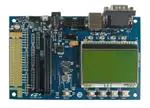
Figure 1. MSC-DBSB8
Software Development Board (SDB)
Figure 2. MSC-DBLB2 (Not Included)
Testing Platform for controlled Lab Tests
(Loadboard)
Both boards come with the Silicon Labs standard 40-pin socket for connecting standard EZRadio® and
EZRadioPRO™ evaluation testcards such as the Si4432-DKDB1. The onboard C8051F930 comes preloaded with
sample firmware to demonstrate a packet-based wireless link between two systems.
The MSC-DBSB8 C8051F9xx software development board includes:
One 40-pin socket for EZRadio and EZRadioPRO testcards
C8051F930 microcontroller preloaded with demonstration software
Standard debug connector for Silicon Labs C8051 programming and debugging
4 buttons and 4 LEDs for custom purposes
LCD display for setup parameters and information display
RS232 interface via a 9-pin DSUB male connector
USB type B connector with Silicon Labs CP2102 USB > Serial Converter onboard
On board 3.3 V PSU
5 x 19 through hole breadboard area for customer's application
Rev. 0.4 8/09
Copyright © 2009 by Silicon Laboratories
SDBC-DK3 UG
�SDBC-DK3 UG
2
Rev. 0.4
�SDBC-DK3 UG
TABLE O F C ONTENTS
Section
Page
1. Introduction . . . . . . . . . . . . . . . . . . . . . . . . . . . . . . . . . . . . . . . . . . . . . . . . . . . . . . . . . . . . .1
2. Power Supply . . . . . . . . . . . . . . . . . . . . . . . . . . . . . . . . . . . . . . . . . . . . . . . . . . . . . . . . . . . .5
2.1. On Board PSU . . . . . . . . . . . . . . . . . . . . . . . . . . . . . . . . . . . . . . . . . . . . . . . . . . . . . .5
2.2. External PSU . . . . . . . . . . . . . . . . . . . . . . . . . . . . . . . . . . . . . . . . . . . . . . . . . . . . . . . .5
2.3. Powered by USB Port . . . . . . . . . . . . . . . . . . . . . . . . . . . . . . . . . . . . . . . . . . . . . . . . .5
3. System Introduction: MSC-DBSB8 ICD Connector . . . . . . . . . . . . . . . . . . . . . . . . . . . . . .6
4. System Introduction: Schematic (MSC-DBSB8) . . . . . . . . . . . . . . . . . . . . . . . . . . . . . . . .8
5. Typical Testboard Schematic (Si443x Testcard) . . . . . . . . . . . . . . . . . . . . . . . . . . . . . . . 10
6. Using the SDB with a Standard Testcard . . . . . . . . . . . . . . . . . . . . . . . . . . . . . . . . . . . . . 11
7. Radio Evaluation . . . . . . . . . . . . . . . . . . . . . . . . . . . . . . . . . . . . . . . . . . . . . . . . . . . . . . . . 12
7.1. Demonstration Mode . . . . . . . . . . . . . . . . . . . . . . . . . . . . . . . . . . . . . . . . . . . . . . . . .12
7.1.1. Packet Error Rates (PER) . . . . . . . . . . . . . . . . . . . . . . . . . . . . . . . . . . . . . . . . . 12
7.1.2. Screen 2: Setting Up the RF Parameters . . . . . . . . . . . . . . . . . . . . . . . . . . . . . 14
7.1.3. Screen 3: Setting up Further RF Parameters . . . . . . . . . . . . . . . . . . . . . . . . . . 14
7.1.4. Understanding Antenna Diversity and Where to Use It . . . . . . . . . . . . . . . . . . . 16
7.1.5. Packet Length . . . . . . . . . . . . . . . . . . . . . . . . . . . . . . . . . . . . . . . . . . . . . . . . . . 17
7.1.6. Max Packets . . . . . . . . . . . . . . . . . . . . . . . . . . . . . . . . . . . . . . . . . . . . . . . . . . . 18
7.1.7. Screen 5: The Ready Screen . . . . . . . . . . . . . . . . . . . . . . . . . . . . . . . . . . . . . .18
7.1.8. Running the Demonstration . . . . . . . . . . . . . . . . . . . . . . . . . . . . . . . . . . . . . . . . 20
7.2. Lab Mode . . . . . . . . . . . . . . . . . . . . . . . . . . . . . . . . . . . . . . . . . . . . . . . . . . . . . . . . . 22
7.2.1. Transmitter Evaluation Setup . . . . . . . . . . . . . . . . . . . . . . . . . . . . . . . . . . . . . .26
7.2.2. Receiver Evaluation Setup . . . . . . . . . . . . . . . . . . . . . . . . . . . . . . . . . . . . . . . . 26
7.2.3. Transmitter Measurements . . . . . . . . . . . . . . . . . . . . . . . . . . . . . . . . . . . . . . . . 26
7.2.4. Results (CW Tests) . . . . . . . . . . . . . . . . . . . . . . . . . . . . . . . . . . . . . . . . . . . . . .29
7.2.5. PN9 Measurement . . . . . . . . . . . . . . . . . . . . . . . . . . . . . . . . . . . . . . . . . . . . . . 30
7.2.6. Results (PN9 Tests) . . . . . . . . . . . . . . . . . . . . . . . . . . . . . . . . . . . . . . . . . . . . .32
7.2.7. Receiver Measurements . . . . . . . . . . . . . . . . . . . . . . . . . . . . . . . . . . . . . . . . . .33
7.2.8. Results (BER Test) . . . . . . . . . . . . . . . . . . . . . . . . . . . . . . . . . . . . . . . . . . . . . .35
7.2.9. Packet Error Test . . . . . . . . . . . . . . . . . . . . . . . . . . . . . . . . . . . . . . . . . . . . . . .36
7.2.10. Results (PER Test) . . . . . . . . . . . . . . . . . . . . . . . . . . . . . . . . . . . . . . . . . . . . .38
7.3. Additional Information . . . . . . . . . . . . . . . . . . . . . . . . . . . . . . . . . . . . . . . . . . . . . . . . 39
7.3.1. USB Communications . . . . . . . . . . . . . . . . . . . . . . . . . . . . . . . . . . . . . . . . . . . . 39
7.3.2. Packet Structure . . . . . . . . . . . . . . . . . . . . . . . . . . . . . . . . . . . . . . . . . . . . . . . . 40
8. Custom Software Development . . . . . . . . . . . . . . . . . . . . . . . . . . . . . . . . . . . . . . . . . . . . 41
8.1. Program Structure . . . . . . . . . . . . . . . . . . . . . . . . . . . . . . . . . . . . . . . . . . . . . . . . . . . 41
8.1.1. Basic Code Overview . . . . . . . . . . . . . . . . . . . . . . . . . . . . . . . . . . . . . . . . . . . .45
8.2. Basic Hardware Connections . . . . . . . . . . . . . . . . . . . . . . . . . . . . . . . . . . . . . . . . . . 46
9. Main . . . . . . . . . . . . . . . . . . . . . . . . . . . . . . . . . . . . . . . . . . . . . . . . . . . . . . . . . . . . . . . . . . . 47
9.1. Flow Chart Main ( ) . . . . . . . . . . . . . . . . . . . . . . . . . . . . . . . . . . . . . . . . . . . . . . . . . . 47
9.2. Main Source File . . . . . . . . . . . . . . . . . . . . . . . . . . . . . . . . . . . . . . . . . . . . . . . . . . . . 48
10. Si4432 . . . . . . . . . . . . . . . . . . . . . . . . . . . . . . . . . . . . . . . . . . . . . . . . . . . . . . . . . . . . . . . . 53
Rev. 0.4
3
�SDBC-DK3 UG
10.1. Flow Chart . . . . . . . . . . . . . . . . . . . . . . . . . . . . . . . . . . . . . . . . . . . . . . . . . . . . . . . .55
10.1.1. RF Packet Received( ) . . . . . . . . . . . . . . . . . . . . . . . . . . . . . . . . . . . . . . . . . . 55
10.1.2. RFTransmit( ) . . . . . . . . . . . . . . . . . . . . . . . . . . . . . . . . . . . . . . . . . . . . . . . . . 55
10.2. Si4432 Header File . . . . . . . . . . . . . . . . . . . . . . . . . . . . . . . . . . . . . . . . . . . . . . . . .56
10.3. Si4432 Source File . . . . . . . . . . . . . . . . . . . . . . . . . . . . . . . . . . . . . . . . . . . . . . . . . 60
11. C8051 . . . . . . . . . . . . . . . . . . . . . . . . . . . . . . . . . . . . . . . . . . . . . . . . . . . . . . . . . . . . . . . . . 67
11.1. C8051 Header File . . . . . . . . . . . . . . . . . . . . . . . . . . . . . . . . . . . . . . . . . . . . . . . . . 67
11.2. C8051 Source File . . . . . . . . . . . . . . . . . . . . . . . . . . . . . . . . . . . . . . . . . . . . . . . . . 70
12. Troubleshooting . . . . . . . . . . . . . . . . . . . . . . . . . . . . . . . . . . . . . . . . . . . . . . . . . . . . . . . .73
Document Change List . . . . . . . . . . . . . . . . . . . . . . . . . . . . . . . . . . . . . . . . . . . . . . . . . . . . .74
Contact Information . . . . . . . . . . . . . . . . . . . . . . . . . . . . . . . . . . . . . . . . . . . . . . . . . . . . . . . .76
4
Rev. 0.4
�SDBC-DK3 UG
2. Power Supply
The board has three power options. The user can select between these options by the supply source selector
switch (SW1).
2.1. On Board PSU
The on board PSU supplies 3.3 VDC. In this mode, the board should be powered by a standard 9 V ac or 9–12 V
dc adapter.
2.2. External PSU
In this mode, the board can be powered via the direct dc supply connector by an external PSU. Any supply voltage
can be used in the 3.3–4 V range. Polarity is marked on the PCB.
2.3. Powered by USB Port
In this mode, the board can be powered via the USB connector.
Note: When using the white LED Flash option, it is recommend to use an alternative power supply.
Rev. 0.4
5
�SDBC-DK3 UG
3. System Introduction: MSC-DBSB8 ICD Connector
Table 1. Debug Connector
Pin #
Description
1
VDD (3.3 V)
2
GND
3
GND
4
P2.7
5
RESET
6
P2.7
7
RST/C2CK
8
—
9
GND
10
—
Figure 3. Debug Connector (Emulator and Programmer Interface)
6
Rev. 0.4
�SDBC-DK3 UG
Table 2. 40-Pin Testcard Connector (J5)
Pin #
Description
Pin #
Description
1
J6/1 (SPI_MOSI)
21
GND
2
J7/1
22
J15/1
3
J6/2 (SPI_SCK)
23
GND
4
J7/2
24
J15/2
5
J6/3 (RF_NSEL)
25
J8/1
6
J7/3
26
EBID port (SPI_MOSI)
7
J6/4
27
GND
8
J7/4
28
EBID port (SPI_MISO)
9
J6/5
29
J8/2
10
J7/5
30
EBID port (SPI_SCK)
11
J6/6
31
GND
12
J7/6 (RF_NIRQ)
32
EBID port (EE_NSEL)
13
J6/7 (PWRDN)
33
J8/3
14
J7/7(RF_NIRQ)
34
J15/3
15
J6/8 (GPIO)
35
GND
16
J7/8(SPI_MISO
36
J15/4
17
VDD (3.3 V)
37
J8/4
18
VDD (3.3 V)
38
J15/5
19
VDD (3.3 V)
39
GND
20
VDD (3.3 V)
40
J15/6
Rev. 0.4
7
�SDBC-DK3 UG
Figure 4. MSC-DBSB8 Schematic (1 of 2)
4. System Introduction: Schematic (MSC-DBSB8)
8
Rev. 0.4
�Figure 5. MSC-DBSB8 Schematic (2 of 2)
SDBC-DK3 UG
Rev. 0.4
9
�SDBC-DK3 UG
Figure 6. Si443x Testcard Schematic
5. Typical Testboard Schematic (Si443x Testcard)
10
Rev. 0.4
�SDBC-DK3 UG
6. Using the SDB with a Standard Testcard
The standard EZRadio or EZRadioPRO testcards that are typically plugged into the MSC-DBLB2 Loadboard when
engineers are performing RF tests on the radio ICs can also be plugged into the 40pin socket on the Software
Development Board (SDB), as demonstrated below.
Figure 7. Software Development Board (MSC-DBSB8)
with a Standard Silicon Labs Testcard Installed
Rev. 0.4
11
�SDBC-DK3 UG
7. Radio Evaluation
7.1. Demonstration Mode
When shipped, the MSC-DBSB8 comes with example firmware, which is used to demonstrate the basic RF
capabilities of Silicon Labs’ RFIC. In the current public release of this firmware only the EZRadioPRO Si4432
transceiver is supported, later releases are intended to demonstrate the ever increasing number of products from
Silicon Labs.
Newer firmware versions of the factory firmware may be available on the Silicon Labs website or via the WDS
CDROM.
Introducing the PER demonstration (Version 3.xr Firmware)
Reference firmware v3.xr is designed to show the Si443x in a packet error rate test demonstration. This firmware is
preloaded on to the c8051F930 microcontroller, but it is also available on the WDS CD-ROMs in the SDB section.
Source code to the Silicon Lab's firmware is also available in the same location, and is provided AS-IS for
reference purposes.
7.1.1. Packet Error Rates (PER)
Packet Errors are common place in wireless communications. In real life applications, these errors are handled
through the use of acknowledgements and retries. In the demonstration software such techniques are NOT
implemented such that system designers can understand range limitations in various environments, allowing them
to design robust protocols into their designs.
In order to use this demonstration, users should start the demo then move the two boards apart until packet errors
can be seen to start appearing and the average PER is in the order of 5%. At this point, the PER demonstration
should be cleared, and the test should be left alone to be re-run without being disturbed. It is expected that the
PER % will be reduce since the environmental factors will be more constant. Re-run the previous steps until a 2–
3% PER is found regularly at a given range. At this point, and with the current environmental conditions, you are at
a range where a higher level protocol is required. Silicon Labs has found that at a low datarate and sending
approximately 5000 packets, a 2–3 km range is attainable.
The demonstration shown below was performed along the Danube River in Budapest, Hungary using the Si4432.
Data rate
Range
2.4 kbps
2.05 km
4.8 kbps
2.03 km
9.6 kbps
1.5 km
50 kbps
1.37 km
100 kbps
1.1 km
125 kbps
0.96 km
Figure 8. Example Range-vs.-Data Rate
Location: Danube River in Budapest, Hungary
12
Rev. 0.4
�SDBC-DK3 UG
Note: The following screen shots reference firmware version 3.5r, screen shots may differ slightly from the version you have
received.
Figure 9. Welcome Screen
Users may by pass the introduction screen by pressing any of the pushbutton 1-4, alternatively wait until the screen
times out and moves on itself.
The following screen allows users to select the mode of operation:
Figure 10. Operating Modes
Figure 11. Screen 1: Demonstration Mode
Since the SDB's firmware recognized the Si4432 test card inserted into the 40 pin socket the appropriate modes of
operation are presented on the menu system—in this case TRx (Transceiver). It is possible however to operate a
transceiver in a RX (Receive) or TX (Transmit) mode also so menu features allow users to override the
functionality. Menu's are driven through the push button's 1–4 under the LCD—the function of each button is shown
on the screen.
Figure 12. Push Buttons and LCD Labeling
Rev. 0.4
13
�SDBC-DK3 UG
The Up/Down button (PB1) moves the arrow up and down the LCD screen.
Figure 13. Active Menu Item Pointer
The arrow is used to highlight the function that will change when the user presses the '+' and '-' buttons. In the
screen shown above, 'Function:' is highlighted, pressing the '+' and '-' buttons will switch the mode of operation
between demonstration mode and lab mode.
Moving the arrow down to the ' =>Demo Mode: TRx' will allow the user to change between TRx, RX and TX
functionality via the '+' and '–' buttons.
For the purpose of this introduction to the system we shall operate in 'Demonstration Mode'. Please ensure Demo
mode is selected and TRx is enabled. The same selections should be made on both of the software development
boards.
7.1.2. Screen 2: Setting Up the RF Parameters
Figure 14. Screen 2: RF Parameters Menu
The 2nd screen sets up the RF parameters for the link. Adjustments are made by scrolling up and down the LCD
using PB1, highlighting the relevant item to be changed and using the '+' and '-' buttons accordingly.
This introduction assumes the following settings:
Data Rate:
2.4 kbps
Modulation:
GFSK
Frequency:
868.00 MHz
The same selections should be made on both of the software development boards.
7.1.3. Screen 3: Setting up Further RF Parameters
On this screen, there may be a difference with respect to the screen shot available which is dependent on the
testcard installed in to the 40 pin connector. Several testcard options are available for the SDBC-DK3 (see website
for details). Typically, testcard variants include antenna diversity cards for use with antennas, single-ended Tx/Rx
testcards (also intended for use with antennas), and split Tx/Rx testcards designed for use with coaxial cable to lab
equipment (see "7.2. Lab Mode" on page 22 for more details).
14
Rev. 0.4
�SDBC-DK3 UG
Figure 15. Antenna Diversity Testcard (May be Ordered Separately)
Figure 16. Split TX and RX Testcard (Rx: Left SMA, Tx: Right SMA) for Use with Coaxial Cable and
RF Test Equipment for Scientific RF Evaluation (May be Ordered Separately)
Figure 17. Single-Ended TX and RX Testcard
Rev. 0.4
15
�SDBC-DK3 UG
If an Antenna Diversity card is fitted then the 'Antenna Mode' option on the 3rd screen will be available, this line is
automatically removed when non-antenna diversity cards such as the 4432-DKDB1 are inserted. With this options
users have the ability to select antenna 1, antenna 2 or both (antenna diversity enabled). For typical operation
select “1&2”.
This screen also allows users to setup the PA output levels of the of the radio. Figure 18 demonstrates an output
power of +20 dBm selected.
Figure 18. Screen 3: RF Parameters (Antenna Diversity Card Fitted)
7.1.4. Understanding Antenna Diversity and Where to Use It
Antenna Diversity is a technique that is use to improve the quality and reliability of a wireless link. The technique is
particularly useful in city-like urban and indoor environments where clear lines of sight between the transmitter and
the receiver cannot be achieved.
In environments where clear lines-of-sight (LOS) are not possible, signals reflect along multiple pathways
(multipath) before being received, each reflection can introduce phase shifts, time delays, attenuations and
distortions that can disrupt the quality of the signal which can cause problems for the receiver. Antenna diversity
assists the receiver by allowing it to see the signal from two slightly different positions through the use of multiple
antennas. Studies have shown that antenna diversity in both indoor and urban environments can recover 8–10 dB
of the link budget that is usually lost to the environment when receivers use only single antenna implementations.
The technique however does not provide any major benefits in open environments and often this misunderstanding can cause confusion during range test exercises. In fact, due to the extra components used in the
antenna switch it is possible that there maybe a small addition loss in the link budget thus reducing range. See
Table 3 and Table 4.
Table 3. Illustrative Effects of Antenna Diversity in Indoor/Urban—Multipath Environments
Single Antenna Implementation
Multiple Antenna Implementation
Transmit Power
+20 dBm
+20 dBm
Receive Sensitivity
–118 dBm
–118 dBm
Multipath Losses
–10 dBm
–2 dBm
Loss in Matching/Switch
–2 dBm
–3 dBm
Link Budget
126 dBm
133 dBm
Table 4. Effects of Antenna Diversity in Line of Sight (LOS)—Open Air Environments
Single Antenna Implementation
Multiple Antenna Implementation
Transmit Power
+20 dBm
+20 dBm
Receive Sensitivity
–118 dBm
–118 dBm
Multipath Losses
0 dBm
0 dBm
Loss in Matching/Switch
–2 dBm
–3 dBm
Link Budget
136 dBm
135 dBm
16
Rev. 0.4
�SDBC-DK3 UG
It can be seen from Table 3 and Table 4 that while the effects of antenna diversity on LOS environments are
negligible, the benefits in indoor/urban environments can significantly help create robust, higher quality robust
links.
Figure 19. Screen 4: Setting Up the Node Parameters
The Self ID on each card should already be selected and is contained in the EBID eeprom on the testcard. The
EBID is placed on the testcard so that our firmware and support GUI's (such as WDS) can recognize the
characteristics of the board. The EBID is NOT required as part of the bill-of-materials in an end customers design.
The EBID contains information such as the local ID, destination ID, matching network configuration and antenna/
test card configuration type.
Figure 20. Test Card Characteristics EEPROM (EBID)
The SDBC-DK3 is initially configured with the same value for the destination ID and the self ID. In order to run the
demo, you will need to configure the destination ID of the first board to that of the second and vice versa. This will
allow the two SDB boards to communicate with each other. The ID is considered the address.
7.1.5. Packet Length
The node parameters screen also allows users to adjust the packet length so that they may:
1. Perform head-to-head comparisons with competitive radios
2. Learn the effects of packet length with respect to data-rate and robustness
Many things affect the robustness of a radio link and often the lack of understanding of some of these variables can
skew test results quite substantially.
A good example of when this misunderstanding takes place is during head to head comparisons of different radio
IC suppliers. By using the 'packet length' option in the menu, users may adjust the length of the packet to match
such that they are looking at the same packet structure during their tests. (See section 7.7 for further details on the
packet structure)
Once designers are satisfied with their head-to head comparisons of the radio IC's having based their tests on
similar structures then designers can use the packet length option to experiment with their protocol. Packet length
can have many tradeoffs with respect to power savings, robustness, data rates, processing overheads, etc.
Rev. 0.4
17
�SDBC-DK3 UG
Consider the following:
During the transmission of long packets, there is an increased chance that a disturbance may occur somewhere
along that packet—thus the need to implement good CRC checks.
During the transmission of short packets, there is an increased chance that the entire packet may be lost during
a disturbance—thus the need to implement more retries.
Transmission of long/short packets with a slow data rates have good easily recognizable 1's and 0's but by
comparison to fast data rates have a greater 'on time' and may use more power but retries may be less (in turn
saving power).
Transmission of long/short packets with a fast data rate may have a less 'on time' but retires may be greater,
antenna diversity may help reduce the multipath effects.
The trade offs in radio applications are many and the list above is by no means the only possible scenarios, every
application has its own list of acceptable trade offs and through the use of menu options such as data-rate, packet
length and antenna diversity engineers can learn to best understand what options work for them and their
environments.
7.1.6. Max Packets
So that designers can scientifically qualify the aforementioned trade offs, careful experimentation in applicable
application-like environments is recommended, the 'Max. Packets' menu option allows designers to select the
number of packets used to generate a Packet Error Rate (PER) result.
A large number of packets (1000–9999) allows for a good averaged result but can take time particularly at low
data rates.
A small number of packets (100) allows for a quick environmental assessment to be made prior to an
exhaustive test.
7.1.6.1. Example—Typical Usage
The designer will arrive at their test site and run a 100 packet test experiment prior to exhaustive testing. If the
results are in accordance with previous tests then the environment is similar to those of the previous occasion. If
there is a substantial difference in the results of a 100 packet test with any previous occasions results then new
environmental factors are playing into tests and these should be recorded as comments so that results from
exhaustive testing is better understood.
.
7.1.7. Screen 5: The Ready Screen
The ready screen on the LCD is the final step before starting your experimentation. The ready screen labels the
LEDs 1–4 according to the function they will perform. In this demonstration they are TX, RX, Antenna 1 and
Antenna 2. Note if you have disabled any of the antenna's or are using a none antenna diversity card then the
associated antenna is not represented by the LEDs.
Figure 21. Non-Antenna Diversity Testcard
Note: Only one antenna highlighted on the top row and NO-ANTDIV shown in the second line of text.
18
Rev. 0.4
�SDBC-DK3 UG
Figure 22. Antenna Diversity Testcard
Note: Depending on antenna selection the relevant antennas are shown on the top row and either ANTDIV, A_DIV(1), or
A_DIV(2) is shown in the second line of text.
The ready screen is designed to allow you to review the settings on both boards. In the example shown above, we
illustrate the following configuration:
Our first board with ID 091 is sending its message to board with the ID 094
At 2.4 kbps
With frequency 868.00 MHz
Using the ready screen, we can see that there is an error on the split TX/RX board in that it is configured with a
selfID of 054, this does not match the DestinationID on the antenna diversity board. From the 'ready screen' we
can update the antenna diversity board accordingly. To do this, we can press PB3 or PB4, which are highlighted as
'SETTINGS' where we can re-run the setting accordingly.
Once the settings are correct we can run the demonstration accordingly.
If the user has the ability to see both ends of the link then a white LED driver is made available on the SDB with
which you can enable a high brightness LED to make visual confirmation easier of the remote board.
Rev. 0.4
19
�SDBC-DK3 UG
Figure 23. White LED Control
This feature is only manually enabled since the brightness of the LED may be distracting when on desk operation
is being implemented.
7.1.8. Running the Demonstration
Longer tests provide better averages, but in the interest of time, this demonstration sends only 1000 packets.
Users that modify the code can send as many or as few packets as they wish. The fact only 1000 packets are sent
can cause higher PER percentages since most of the dropped packets will occur while the user is setting up the
demonstration because he himself will absorb much of the radiation and add to multipath and fading effects. As
users become more familiar with radio it is highly recommended a greater number of packets be sent such that a
better average can be generated.
To run the demonstration, place one SDB in a fixed location. (If testing an antenna diversity system, place the
antenna diversity unit in the fixed location while using a single-ended testcard as the roaming testcard). The SDB
kept in the fixed location should be considered the “base unit”. This unit will act as the base unit. On the mobile
unit, the unit with the split TX and RX, press 'TX ON' and walk away from the base unit until the PER settles around
5-7%. When the PER has settled and all 1000 packets are sent press the CLEAR button and run the test again but
avoid being to close to the demo during the second test. If the test completes with 0-2% PER then the test should
be run again with a greater range, if 4–6% then run again but with a lower range. Once you reliably get 2-3% at the
end of the series of tests then, in that environment this can be considered the typical range in an application with
limited error handling - as is the purpose of this experiment.
Good protocols and handling of dropped packets enable users to get much greater ranges.
During early experimentation, users may notice that the LCD and LEDs show information that represents antenna
strength.
20
Rev. 0.4
�SDBC-DK3 UG
Figure 24. Active Antenna and RSSI Indications
Rev. 0.4
21
�SDBC-DK3 UG
7.2. Lab Mode
The lab mode is intended for users who want to evaluate the performance of the Silicon Labs RFICs, supported
through the shipping factory firmware on the SDB platform.
Lab mode is intended so users can perform simple evaluations, such as:
Transmitter Evaluation
Output
power
analysis
Spectrum
Receiver Evaluation
BER
Sensitivity
Sensitivity
Receiver parameters:
Automatic Frequency Control
Blocking
Selectivity
PER
Using lab mode, users can independently evaluate transmit and receive performance. Table 5 lists the test cards
available for ordering.
Table 5. Test Cards Available for Ordering
Type
Matching Network
Configuration
Part Number
Transceivers
High band
4432 – DKDB1
4431 – DKDB1
Low band
4432 – DKDB5
4431 – DKDB5
Receivers
Transmitters
High band
4330 – DKDB1
Low band
4330 – DKDB5
High band
4032 – DKDB1
4031 – DKDB1
Low band
4032 – DKDB5
4031 – DKDB5
22
Rev. 0.4
�SDBC-DK3 UG
RX Connection
TX Connection
Figure 25. 4432-DKDB1 - Split TX/RX Antenna Card Using Coaxial Cable
Rev. 0.4
23
�SDBC-DK3 UG
Figure 26. Lab Equipment Connection Diagram
24
Rev. 0.4
�SDBC-DK3 UG
Figure 27. Test Card Connection Diagram
Figure 28. SDB Connection Diagram
Rev. 0.4
25
�SDBC-DK3 UG
7.2.1. Transmitter Evaluation Setup
The transmitter output of the 4432-DKDB1 test board can be connected to a spectrum analyzer in order to evaluate
output power and spectrum plots. Alternatively the transmitter output may be connected to a vector signal analyzer
to evaluate conditions such as freq vs time.
The 4432-DKDB1 testcard also provides access to the radio's GPIO which can be used as test-points for the radios
internal signals - see diagram above.
7.2.2. Receiver Evaluation Setup
Receiver evaluation can be performed by connecting the receiver port of the testcard to an RF signal generator.
The RF generator may use a data source from an external IQ generator or from its internal memory depending on
its feature set, often RF generators have a PN9 pattern option.
The 4432-DKDB1 testcard also provides access to the radio's GPIO which can be used as test-points for the radios
internal signals - see test card connection diagram.
Two modes are typically used during evaluations:
1. Direct Mode: In this mode, data is continuously sent via a source such as a PN9 generator.
2. Packet Mode: In this mode, the data source is customized in a defined packet structure.
Typically: Preamble + Sync_Word + Data payload + CRC.
Example of a 20 byte packet that can be received by the SDB firmware:
Preamble:
1010101010101010101010101010101010101010101010101010101010101010
Sync:
0010110111010100
Date:
0001010000110100001100000000100101100110001011111001110101010101
0101011101100001010011110010101111010100010000111101001101000010
1111011110011010011100001001000111000011
CRC :
1101011110011000
7.2.3. Transmitter Measurements
7.2.3.1. CW Lab Mode
Using the CW Lab Mode, users may evaluate the following:
1. Output Power
2. Frequency Offset in Transmitter Output
3. Phase Noise
26
Rev. 0.4
�SDBC-DK3 UG
7.2.3.2. Test Method
Figure 29. Setup Screen (1 of 4)
1. Ensure “Lab Mode” is selected as the operating function.
2. Select CW.
3. Press to move on from this screen.
Figure 30. Setup Screen (2 of 4)
1. Select the appropriate frequency.
When evaluating with CW, data rate and modulation have no effect.
2. Press to move on from this screen.
Rev. 0.4
27
�SDBC-DK3 UG
Figure 31. Setup Screen (3 of 4)
1. Select the appropriate output power required for the test.
2. Press to move on from this screen.
Note: If an alternate testcard is used, such as the antenna diversity test cards, users may see slightly different screen shots
than those shown. Users must turn off the diversity function by selecting “antenna 1” and connecting to the appropriate
antenna connector using 50 coaxial cable.
Figure 32. Setup Screen (4 of 4)
1. Parameters on setup screen 4 are not relevant to CW evaluations. Silicon Labs recommends leaving them at
their default values.
2. Press to move on from this screen.
In Figure 33, the runtime screen will summarize the current valid settings.
Figure 33. Runtime Screen
28
Rev. 0.4
�SDBC-DK3 UG
7.2.4. Results (CW Tests)
7.2.4.1. Output Power
1. Set the center frequency of spectrum analyzer to the frequency under test.
2. Set span to 10 MHz.
3. Measure the TX output power on displayed plot.
Figure 34. Spectrum Plot Showing CW Output at 917 MHz
7.2.4.2. Frequency Offset at Transmitter Output
1. Set the center frequency of spectrum analyzer to the frequency under test.
2. Set span to 100 kHz.
3. Measure the frequency offset between the expected frequency as selected in the menu and the actual TX
output frequency.
Figure 35. Typical Spectrum Plot Using a Silicon Labs Branded Testcard
In Figure 35, it can be seen that the frequency error is less than 1 kHz.
Silicon Labs testcards are designed to have a maximum frequency error of < 5 kHz.
Rev. 0.4
29
�SDBC-DK3 UG
7.2.4.3. Phase Noise
1. Set the Spectrum analyzer to “Phase Noise”.
2. Set the center frequency of spectrum analyzer to the frequency selected.
3. Set the spectrum analyzer to the desired span (typically from 100 Hz to 10 MHz span).
Figure 36. Typical Phase Noise Plot at 917 Mhz
7.2.5. PN9 Measurement
Using the PN9 Lab Mode, users may evaluate the following:
1. Tx output spectrum
2. Transmitter spectral mask
7.2.5.1. Test Method
Figure 37. Setup Screen (1 of 4)
1. Ensure “Lab Mode” is selected as the operating function.
2. Select PN9.
3. Press to move on from this screen.
30
Rev. 0.4
�SDBC-DK3 UG
Figure 38. Setup Screen (2 of 4)
1. Select the appropriate frequency, data rate, and modulation.
2. Press to move on from this screen.
Figure 39. Setup Screen (3 of 4)
1. Select the desired output power.
2. Press to move on from this screen.
Figure 40. Setup Screen (4 of 4)
1. Parameters in Figure 40 are not relevant to PN9 evaluations. Silicon Labs recommends leaving them at their
default values.
2. Press to move on from this screen.
Rev. 0.4
31
�SDBC-DK3 UG
Figure 41. Runtime Screen
In Figure 41, the runtime screen will summarize the current valid settings.
7.2.6. Results (PN9 Tests)
7.2.6.1. TX Output Spectrum
1. Set the center frequency of spectrum analyzer to the frequency under test.
2. Set span to 500 kHz and observe the TX spectrum.
7.2.6.2. Evaluation of TX Spectral Mask
Using the PN9 mode, users can observe the TX spectrum to evaluate FCC/ETSI compliance.
Figure 42. Spectrum Plot Demonstrating 40K Data Rate, 40K Deviation, GFSK Modulation
32
Rev. 0.4
�SDBC-DK3 UG
7.2.7. Receiver Measurements
7.2.7.1. Bit Error Rate Test
Using the BER Lab Mode users may evaluate the following:
1. BER Sensitivity.
2. Direct mode operation using a continuous data streams
3. Receiver modem parameters:
i. Automatic Frequency Control
ii. Blocking
iii. Selectivity
7.2.7.2. Test Method
1. Set frequency, modulation type, data rate and deviation parameters on the RF signal generator.
2. Select the desired data source for the RF generator (e.g. PN9)
3. Connect the receiver's input to the signal generator's output.
Figure 43. Setup Screen (1 of 4)
1. Ensure Function is set to “Lab”
2. Set Lab Mode to “BER”
3. Press to move on from this screen.
Figure 44. Setup Screen (2 of 4)
1. Selections here should match those previously entered into the RF Signal Generator
2. Press to move on from this screen.
Rev. 0.4
33
�SDBC-DK3 UG
Figure 45. Setup Screen (3 of 4)
1. Parameters on setup screen 3 are not relevant to BER evaluations. Silicon Labs recommends leaving them at
their default values.
2. Press to move on from this screen.
Figure 46. Setup Screen (4 of 4)
1. Parameters on setup screen 4 are not relevant to BER evaluations. Silicon Labs recommends leaving them at
their default values
2. Press to move on from this screen
Figure 47. Runtime Screen
In the Figure 47, the runtime screen will summarize the current valid settings.
34
Rev. 0.4
�SDBC-DK3 UG
7.2.8. Results (BER Test)
7.2.8.1. BER Sensitivity Evaluation
BER results will be shown on the BER instrument or recorded by either RF generators or IQ modulators that have
a BER option installed.
The top trace in Figure 48 demonstrates TX_Data as sent by a transmitter and the bottom trace is the data
received on the GPIO pin. Please note that there is an expected shift caused by a delay between the data at the
transmitter and the data received by the receiver.
Figure 48. TX Data Sent and Received
7.2.8.2. Other Receiver Measurements
Using the test setup described above, users may also perform Automatic Frequency Control (AFC), Blocking and
Selectivity tests. All the required parameters are controlled by the external RF generator.
Rev. 0.4
35
�SDBC-DK3 UG
7.2.9. Packet Error Test
Using the PER Lab Mode users may evaluate the following:
1. PER Sensitivity
2. FIFO mode using predefined packet structures (see data sheet for further details)
3. Receiver modem parameters:
i. Automatic Frequency Control
ii. Blocking
iii. Selectivity
4. Connect the receiver's input to the signal generator's output.
7.2.9.1. Test Method
1. Set frequency, modulation type, data rate and deviation parameters on the RF signal generator.
2. Program a predefined packet into the generator using the format:
(preamble + sync_word(2DD4H) + data + CRC).
3. Set the signal generator to external single trigger mode.
4. The software development board (SDB) generates a trigger on test point P1.4, this should be connected to the
RF signal generator's external trigger input. The P1.4 pin will enable the signal generator to send one packet for
each trigger.
Figure 49. Setup Screen (1 of 5)
1. Ensure Function is set to “Lab”
2. Set Lab Mode to “PER”
3. Press to move on from this screen.
Figure 50. Setup Screen (2 of 5)
1. Selections here should match those previously entered into the RF Signal Generator.
2. Press to move on from this screen.
36
Rev. 0.4
�SDBC-DK3 UG
Figure 51. Setup Screen (3 of 5)
1. Parameters on setup screen 4 are not relevant to PER evaluations. Silicon Labs recommends leaving them at
their default values.
2. Press to move on from this screen.
Figure 52. Setup Screen (4 of 5)
1. Ensure the Packet length matches that programmed in the RF signal generator.
2. Select number of packets to be received by the receiver using the Max. Packets field. The appropriate number
of triggers will be sent by the SDB according to this setting.
3. Press to move on from this screen.
Figure 53. Setup Screen (5 of 5)
1. Press to commence packet error rate evaluation.
This will start generating pulses on P1.4 that are used to trigger the RF signal generator. The RF generator will
send one packet for every external trigger. As the radio is set to receive mode it is waiting for a specific preprogrammed packet to be arrive at the pre-programmed frequency, modulation and data rate.
Rev. 0.4
37
�SDBC-DK3 UG
Figure 54. Runtime Screen
In Figure 54, the runtime screen will summarize the current valid settings.
Notes:
1. TR = Trigger sent on P1.4.
2. MP = Missed packets
3. PER = Packet error rate
7.2.10. Results (PER Test)
7.2.10.1. PER Measurement
The result of PER measurement is shown on the LCD display. Connecting to the GPIO and the trigger the user can
see the following signals.
Figure 55.
In Figure 55, the top trace shows the trigger provided on P1.4 of the SDB, the middle trace shows the received
data and the bottom trace shows the transmitted data from the RF signal generator.
In the plot we can see the receiver is turned on before the packet arrived. Once the valid packet is received the
radio will return to tune mode. The radio will switch to receive mode prior to sending the next trigger. This is
repeated for the value set in “Max. Packets”.
7.2.10.2. Other Receiver Measurements:
Using the test setup described above, users may also perform Automatic Frequency Control (AFC), Blocking and
Selectivity tests. All the required parameters are controlled by the external RF generator.
38
Rev. 0.4
�SDBC-DK3 UG
7.3. Additional Information
7.3.1. USB Communications
To enable greater analysis of the data information regarding the test is sent out over the USB and can be viewed
via a serial terminal emulator such as the WDS Terminal Emulator found on the WDS CDROM.
To configure the MSC-DBSB8 software development board to communicate with a PC via the USB port, a virtual
serial port driver needs to be installed on the PC.
When the MSC-DBSB8 is connected, you may be prompted to install the Virtual COM port driver.
This driver can be found on the WDS CDROM.
The Virtual COM port settings of the software development board are as follows:
Data rate is 19.2 kbps
1 stop bit
No parity bit
No handshake
If USB to virtual serial port driver is installed correctly, when the software development board is connected to PC by
USB port and the WDS Terminal Emulator is running, test results like following can be seen in Figure 56.
Figure 56. Figure 3:Test Result Displayed by USB Virtual COM Port
Rev. 0.4
39
�SDBC-DK3 UG
7.3.2. Packet Structure
The packet structure used by this demonstration is very simple but is not much different than a typical packet found
in many RF applications today.
Figure 57. Packet Format Defined in the Packet Error Rate Test
40
Rev. 0.4
�SDBC-DK3 UG
8. Custom Software Development
Initially the SDBC-DK3 Software Development Kit offers the ability to become acquainted with the basic capabilities
of the EZRadioPRO product family, however, the kit is also designed to be used for basic code development on any
of the RF products offered by Silicon Laboratories. By design, the kit offers two modes of operation; demonstration
mode or lab mode.
The source code to the factory firmware is available on the WDS CDROM but may be somewhat complex for use
as reference code. To aid in software development the following chapter maybe used to illustrate basic code
segment to create RF links using the EZRadioPRO platform.
The code set forth in the following chapter demonstrates a simple push button application and is based upon the
EZRadioPRO Si443x transceiver using the C8051F930 microcontroller.
8.1. Program Structure
Program Start
Main ( )
MCU
Hardware
Initialization
RF Hardware
Initialization
I/O port definition
System Clock
Init
Hardware SPI
Initialization
Read and Clear all Interrupt
Status Registers
Registers: 0x03, 0x04
Software
reset the chip
?
SW Reset
Register: 0x07
Is the chip in
ready ?
Wait for chip to be in ready mode ‘ichipready’
Registers: 0x05, 0x06, 0x03, 0x04
Figure 58. Basic Program Structure Block Diagram (1 of 4)
Rev. 0.4
41
�SDBC-DK3 UG
Chip version
V2
?
TX/RX
offset?
Set VCOCurrentTrimming,
DividerCurrentTrimmingAGCOveride, and
DeltasigmaADCTuning value for optimization
specific to chip version
Registers: 0x5A, 0x59, 0x6A, 0x68
Set capacitance bank to
adjust the offset
Register: 0x09
Set center frequency of operation
Register: 0x75, 0x76, 0x77
Use TX/RX
header ?
Set TX/RX Header for header
check
Register: 0x32, 0x33
Customize Sync
Words?
Set up Sync Words
2&3
Register: 0x37, 0x36
Using GIPOs
?
Configuring GPIOs
Register: 0x0B, 0x0C, 0x0D
Specific Data Rate and
Modem Settings ?
Please use EZRadioPRO Register Calculator
to configures the RF chip’s modem for
different (predefined) data rate, deviation, and
modulation index requirements.
Figure 59. Basic Program Structure Block Diagram (2 of 4)
42
Rev. 0.4
�SDBC-DK3 UG
RF chip in
Idle Mode
Set Register 0x07
( 0x8701 )
RF chip in
Receive
Mode
Set Register 0x07
( 0x8705 )
While (1)
No
Button pushed
?
PB1_PIN == 0
RFPacketReceived
( &packet[0],&length) )
Continuous
receive mode
RFReceive ()
Return:
RF_NO_PACKET
nIRQ
interrupt
occurred?
Return:
RF_NO_PACKET
Read out Interrupt Status
Registers
Read
Registers: 0x03, 0x04
packet
received
interrupt
?
CRC ERROR
interrupt occurred
(ItStatus1 & 0x01) ==
0x01
Yes
Return:
RF_CRC_ERROR
1) strcpy(&packet[0],"PAYLOAD")
Build packet
Packet Received
interrupt occurred
(ItStatus1 & 0x02) == 0x02
RFTransmit
( &packet[0],&length) )
Read Packet Length
Information
Figure 60. Basic Program Structure Block Diagram (3 of 4)
Rev. 0.4
43
�SDBC-DK3 UG
Set Packet Length Information
Set Register 0x3E
DO a Burst Write to FIFO
(