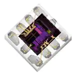
S i 1132
AND
A M B I E N T L I G H T S E NS O R I C
WITH
I 2 C I NT ERF ACE
Features
es
ig
ns
U V I NDEX
Pin Assignments
Integrated UV index sensor
Digital
UV Index register that can
be read through I2C interface
Factory calibration to address
part-to-part variation
Industry's lowest power
consumption
to 3.6 V supply voltage
< 500 nA standby current
Internal and external wake support
Built-in voltage supply monitor and
power-on reset controller
Integrated ambient light sensor
Temperature Range
–40
Applications
SCL
2
VDD
3
INT
4
10
QFN-10
5
9
VDD
8
GND
7
VDD
6
VDD
DNC
Tablets
Portable consumer electronics
Display-backlighting control
m
en
de
d
Fitness/health electronics
Smart watches
Smartphone handsets
to +85 °C
1
N
ew
mlx resolution possible,
2
allowing operation under dark
I C Serial communications
glass
Up to 3.4 Mbps data rate
1 to 128 klx dynamic range
Slave mode hardware address
possible across two ADC range
decoding
settings
Small-outline 10-lead 2x2 mm
Accurate lux measurements with
QFN
IR correction algorithm
SDA
fo
r
100
DNC
1.71
D
Description
N
ot
R
ec
om
The Si1132 is a low-power, ultraviolet (UV) index, and ambient light
sensor with I2C digital interface and programmable-event interrupt output.
This sensor IC includes an analog-to-digital converter, integrated highsensitivity visible and infrared photodiodes, and digital signal processor.
The Si1132 offers excellent performance under a wide dynamic range
and a variety of light sources including direct sunlight. The Si1132 can
also work under dark glass covers. The photodiode response and
associated digital conversion circuitry provide excellent immunity to
artificial light flicker noise and natural light flutter noise. The Si1132
devices are provided in a 10-lead 2x2 mm QFN package and are capable
of operation from 1.71 to 3.6 V over the –40 to +85 °C temperature range.
Rev. 1.2 12/14
Copyright © 2014 by Silicon Laboratories
Si1132
�Si11 32
Functional Block Diagram
Temp
A
M
U
X
Visible
INT
Filter
ADC
Digital Sequencer & Control Logic
Infrared
SCL
Registers
I2C
Oscillator
fo
r
3.3 V
Host
Si1132
SDA
m
en
de
d
SCL
INT
SDA
VDD
SCL
GND
VDD
VDD
INT
VDD
0.1 uF
N
ot
R
ec
om
Figure 1. Si1132 Application
2
GND
N
ew
SDA
es
ig
ns
Regulator
D
VDD
Rev. 1.2
�Si1132
TABLE O F C ONTENTS
N
ot
R
ec
om
m
en
de
d
fo
r
N
ew
D
es
ig
ns
1. Electrical Specifications . . . . . . . . . . . . . . . . . . . . . . . . . . . . . . . . . . . . . . . . . . . . . . . . . . .4
1.1. Performance Tables . . . . . . . . . . . . . . . . . . . . . . . . . . . . . . . . . . . . . . . . . . . . . . . . . .4
1.2. Typical Performance Graphs . . . . . . . . . . . . . . . . . . . . . . . . . . . . . . . . . . . . . . . . . . .8
2. Functional Description . . . . . . . . . . . . . . . . . . . . . . . . . . . . . . . . . . . . . . . . . . . . . . . . . . . .9
2.1. Introduction . . . . . . . . . . . . . . . . . . . . . . . . . . . . . . . . . . . . . . . . . . . . . . . . . . . . . . . . .9
2.2. Ambient Light . . . . . . . . . . . . . . . . . . . . . . . . . . . . . . . . . . . . . . . . . . . . . . . . . . . . . . .9
2.3. Ultraviolet (UV) Index . . . . . . . . . . . . . . . . . . . . . . . . . . . . . . . . . . . . . . . . . . . . . . . . 11
2.4. Host Interface . . . . . . . . . . . . . . . . . . . . . . . . . . . . . . . . . . . . . . . . . . . . . . . . . . . . . . 13
3. Operational Modes . . . . . . . . . . . . . . . . . . . . . . . . . . . . . . . . . . . . . . . . . . . . . . . . . . . . . . . 15
3.1. Off Mode . . . . . . . . . . . . . . . . . . . . . . . . . . . . . . . . . . . . . . . . . . . . . . . . . . . . . . . . . . 15
3.2. Initialization Mode . . . . . . . . . . . . . . . . . . . . . . . . . . . . . . . . . . . . . . . . . . . . . . . . . . . 15
3.3. Standby Mode . . . . . . . . . . . . . . . . . . . . . . . . . . . . . . . . . . . . . . . . . . . . . . . . . . . . . . 15
3.4. Forced Conversion Mode . . . . . . . . . . . . . . . . . . . . . . . . . . . . . . . . . . . . . . . . . . . . .15
3.5. Autonomous Operation Mode . . . . . . . . . . . . . . . . . . . . . . . . . . . . . . . . . . . . . . . . . .16
4. Programming Guide . . . . . . . . . . . . . . . . . . . . . . . . . . . . . . . . . . . . . . . . . . . . . . . . . . . . . . 17
4.1. Command and Response Structure . . . . . . . . . . . . . . . . . . . . . . . . . . . . . . . . . . . . . 17
4.2. Command Protocol . . . . . . . . . . . . . . . . . . . . . . . . . . . . . . . . . . . . . . . . . . . . . . . . . . 18
4.3. Resource Summary . . . . . . . . . . . . . . . . . . . . . . . . . . . . . . . . . . . . . . . . . . . . . . . . . 20
4.4. Signal Path Software Model . . . . . . . . . . . . . . . . . . . . . . . . . . . . . . . . . . . . . . . . . . . 23
4.5. I2C Registers . . . . . . . . . . . . . . . . . . . . . . . . . . . . . . . . . . . . . . . . . . . . . . . . . . . . . . . 24
4.6. Parameter RAM . . . . . . . . . . . . . . . . . . . . . . . . . . . . . . . . . . . . . . . . . . . . . . . . . . . .35
5. Pin Descriptions . . . . . . . . . . . . . . . . . . . . . . . . . . . . . . . . . . . . . . . . . . . . . . . . . . . . . . . . . 42
6. Ordering Guide . . . . . . . . . . . . . . . . . . . . . . . . . . . . . . . . . . . . . . . . . . . . . . . . . . . . . . . . . . 43
7. Package Outline: 10-Pin QFN . . . . . . . . . . . . . . . . . . . . . . . . . . . . . . . . . . . . . . . . . . . . . . 44
8. Suggested PCB Land Pattern . . . . . . . . . . . . . . . . . . . . . . . . . . . . . . . . . . . . . . . . . . . . . . 46
Document Change List . . . . . . . . . . . . . . . . . . . . . . . . . . . . . . . . . . . . . . . . . . . . . . . . . . . . .48
Contact Information . . . . . . . . . . . . . . . . . . . . . . . . . . . . . . . . . . . . . . . . . . . . . . . . . . . . . . . .49
Rev. 1.2
3
�Si11 32
1. Electrical Specifications
1.1. Performance Tables
Symbol
VDD Supply Voltage
Test Condition
VDD
VDD OFF Supply Voltage
VDD_OFF
VDD Supply Ripple Voltage
Typ
Max
Unit
1.71
—
3.6
V
1.0
V
50
mVpp
85
°C
OFF mode
–0.3
VDD = 3.3 V
1 kHz–10 MHz
—
T
–40
SCL, SDA, Input High Logic
Voltage
I2CVIH
SCL, SDA Input Low Logic
Voltage
I2CVIL
Edc
—
VDD
V
0
—
VDDx0.3
V
—
—
128
klx
25
—
—
ms
VDD above 1.71 V
Start-Up Time
25
VDDx0.7
fo
r
Operation under Direct Sunlight
—
N
ew
Operating Temperature
Min
D
Parameter
es
ig
ns
Table 1. Recommended Operating Conditions
Parameter
IDD OFF Mode
IDD Standby Mode
Symbol
Test Condition
Min
Typ
Max
Unit
Ioff
VDD < VDD_OFF (leakage from SCL,
SDA, and INT not included)
—
240
1000
nA
Isb
No ALS Conversions
No I2C Activity
VDD = 1.8 V
—
150
500
nA
Isb
No ALS Conversions
No I2C Activity
VDD =3.3 V
—
1.4
—
µA
Iactive
VDD = 3.3 V
—
4.3
5.5
mA
VDD = 3.3 V
–1
—
1
µA
UV or ALS VIS + ALS IR
—
285
—
µs
om
IDD Standby Mode
m
en
de
d
Table 2. Performance Characteristics1
ec
IDD Actively Measuring
R
INT, SCL, SDA
Leakage Current
Actively Measuring Time2
N
ot
Notes:
1. Unless specifically stated in "Conditions", electrical data assumes ambient light levels < 1 klx.
2. Represents the time during which the device is drawing a current equal to Iactive for power estimation purposes.
Assumes default settings.
4
Rev. 1.2
�Si1132
Table 2. Performance Characteristics1 (Continued)
Typ
Max
Unit
Sunlight
ALS_VIS_ADC_GAIN=0
VIS_RANGE=0
—
0.282
—
ADC
counts/
lux
2500K incandescent bulb
ALS_VIS_ADC_GAIN=0
VIS_RANGE=0
—
“Cool white” fluorescent
ALS_VIS_ADC_GAIN=0
VIS_RANGE=0
—
Infrared LED (875 nm)
ALS_VIS_ADC_GAIN=0
VIS_RANGE=0
—
Sunlight
ALS_IR_ADC_GAIN=0
IR_RANGE=0
0.319
—
ADC
counts/
lux
0.146
—
ADC
counts/
lux
8.277
—
ADC
counts.
m2/W
—
2.44
—
ADC
counts/
lux
—
8.46
—
ADC
counts/
lux
“Cool white” fluorescent
ALS_IR_ADC_GAIN=0
IR_RANGE=0
—
0.71
—
ADC
counts/
lux
Infrared LED (875 nm)
ALS_IR_ADC_GAIN=0
IR_RANGE=0
—
452.38
—
ADC
counts.
m2/W
All gain settings
—
7
—
ADC
counts
RMS
All gain settings
—
1
—
ADC
counts
RMS
fo
r
Small Infrared Photodiode
Response
Min
m
en
de
d
2500K incandescent bulb
ALS_IR_ADC_GAIN=0
IR_RANGE=0
om
Visible Photodiode Noise
ec
Small Infrared Photodiode
Noise
es
ig
ns
Visible Photodiode
Response
Test Condition
D
Symbol
N
ew
Parameter
N
ot
R
Notes:
1. Unless specifically stated in "Conditions", electrical data assumes ambient light levels < 1 klx.
2. Represents the time during which the device is drawing a current equal to Iactive for power estimation purposes.
Assumes default settings.
Rev. 1.2
5
�Si11 32
Test Condition
Min
Visible Photodiode Offset
Drift
VIS_RANGE=0
ALS_VIS_ADC_GAIN=0
ALS_VIS_ADC_GAIN=1
ALS_VIS_ADC_GAIN=2
ALS_VIS_ADC_GAIN=3
ALS_VIS_ADC_GAIN=4
ALS_VIS_ADC_GAIN=5
ALS_VIS_ADC_GAIN=6
ALS_VIS_ADC_GAIN=7
—
Small Infrared Photodiode
Offset Drift
IR_RANGE=0
IR_GAIN=0
IR_GAIN=1
IR_GAIN=2
IR_GAIN=3
—
I = 4 mA, VDD > 2.0 V
I = 4 mA, VDD < 2.0 V
—
—
25 °C
m
en
de
d
Table 2. Performance Characteristics1 (Continued)
SCL, SDA, INT Output Low
Voltage
VOL
Temperature Sensor Offset
Typ
Temperature Sensor Gain
Max
Unit
—
ADC
counts/
°C
D
es
ig
ns
–0.3
–0.11
–0.06
–0.03
–0.01
–0.008
–0.007
–0.008
—
ADC
counts/
°C
—
—
VDDx0.
2
0.4
V
V
—
11136
—
ADC
counts
—
35
—
ADC
counts/
°C
–0.3
–0.06
–0.03
–0.01
N
ew
Symbol
fo
r
Parameter
N
ot
R
ec
om
Notes:
1. Unless specifically stated in "Conditions", electrical data assumes ambient light levels < 1 klx.
2. Represents the time during which the device is drawing a current equal to Iactive for power estimation purposes.
Assumes default settings.
6
Rev. 1.2
�Si1132
Table 3. I2C Timing Specifications
Min
Typ
Max
Unit
Clock Frequency
fSCL
95
—
3400
kHz
Clock Pulse Width Low
tLOW
160
—
—
ns
Clock Pulse Width High
tHIGH
60
—
—
ns
Rise Time
tR
10
—
40
ns
Fall Time
tF
10
—
40
ns
Start Condition Hold Time
tHD.STA
160
—
—
ns
Start Condition Setup Time
tSU.STA
160
Input Data Setup Time
tSU.DAT
Input Data Hold Time
Stop Condition Setup Time
—
ns
10
—
—
ns
tHD.DAT
0
—
—
ns
tSU.STO
160
—
—
ns
Min
Typ
Max
Unit
–0.3
—
4
V
–40
—
85
°C
–65
—
85
°C
at VDD = 0 V, TA < 85 °C
–0.5
—
3.6
V
Human Body Model
Machine Model
Charged-Device Model
—
—
—
—
—
—
2
225
2
kV
V
kV
fo
r
Test Condition
Operating Temperature
Storage Temperature
INT, SCL, SDA Voltage
N
ot
R
ec
om
ESD Rating
m
en
de
d
VDD Supply Voltage
D
—
Table 4. Absolute Maximum Limits
Parameter
es
ig
ns
Symbol
N
ew
Parameter
Rev. 1.2
7
�Si11 32
m
en
de
d
fo
r
N
ew
D
es
ig
ns
1.2. Typical Performance Graphs
N
ot
R
ec
om
Figure 2. ALS Variability with Different Light Sources
8
Rev. 1.2
�Si1132
2. Functional Description
2.1. Introduction
es
ig
ns
The Si1132 is a UV index and ambient light sensor whose operational state is controlled through registers
accessible through the I2C interface. The host can command the Si1132 to initiate on-demand UV index sensing or
ambient light sensing. The host can also place the Si1132 in an autonomous operational state where it performs
measurements at set intervals and interrupts the host after each measurement is completed. This results in an
overall system power saving allowing the host controller to operate longer in its sleep state instead of polling the
Si1132. For more details, refer to “AN498: Si114x Designer’s Guide”.
2.2. Ambient Light
N
ew
D
The Si1132 has photodiodes capable of measuring both visible and infrared light. However, the visible photodiode
is also influenced by infrared light. The measurement of illuminance requires the same spectral response as the
human eye. If an accurate lux measurement is desired, the extra IR response of the visible-light photodiode must
be compensated. Therefore, to allow the host to make corrections to the infrared light’s influence, the Si1132
reports the infrared light measurement on a separate channel. The separate visible and IR photodiodes lend
themselves to a variety of algorithmic solutions. The host can then take these two measurements and run an
algorithm to derive an equivalent lux level as perceived by a human eye. Having the IR correction algorithm
running in the host allows for the most flexibility in adjusting for system-dependent variables. For example, if the
glass used in the system blocks visible light more than infrared light, the IR correction needs to be adjusted.
fo
r
If the host is not making any infrared corrections, the infrared measurement can be turned off in the CHLIST
parameter.
By default, the measurement parameters are optimized for indoor ambient light levels where it is possible to detect
light levels as low as 6 lx. For operation under direct sunlight, the ADC can be programmed to operate in a high
signal operation so that it is possible to measure direct sunlight without overflowing the 16-bit result.
m
en
de
d
For low-light applications, it is possible to increase the ADC integration time. Normally, the integration time is
25.6 µs. By increasing this integration time to 410 µs, the ADC can detect light levels as low as 1 lx. The ADC can
be programmed with an integration time as high as 3.28 ms, allowing measurement to 100 mlx light levels. The
ADC integration time for the Visible Light Ambient measurement can be programmed independently of the ADC
integration time of the Infrared Light Ambient measurement. The independent ADC parameters allow operation
under glass covers having a higher transmittance to Infrared Light than Visible Light.
om
When operating in the lower signal range, or when the integration time is increased, it is possible to saturate the
ADC when the ambient light suddenly increases. Any overflow condition is reported in the RESPONSE register,
and the corresponding data registers report a value of 0xFFFF. Based on either of these two overflow indicators,
the host can adjust the ADC sensitivity. However, the overflow condition is not sticky. If the light levels return to a
range within the capabilities of the ADC, the corresponding data registers begin to operate normally. The
RESPONSE register will continue to hold the overflow condition until a NOP command is received. Even if the
RESPONSE register has an overflow condition, commands are still accepted and processed.
N
ot
R
ec
The Si1132 can initiate ALS measurements either when explicitly commanded by the host or periodically through
an autonomous process. Refer to "3. Operational Modes" on page 15 for additional details of the Si1132's
Operational Modes.
Rev. 1.2
9
�N
ot
10
Rev. 1.2
fo
r
N
ew
es
ig
ns
D
Figure 3. Photodiode Spectral Response to Visible and Infrared Light (Indicative)
m
en
de
d
om
ec
R
Si11 32
�Si1132
2.3. Ultraviolet (UV) Index
m
en
de
d
fo
r
N
ew
D
es
ig
ns
The UV Index is a number linearly related to the intensity of sunlight reaching the earth and is weighted according
to the CIE Erythemal Action Spectrum as shown in Figure 4. This weighting is a standardized measure of human
skin's response to different wavelengths of sunlight from UVB to UVA. The UV Index has been standardized by the
World Health Organization and includes a simplified consumer UV exposure level as shown in Figures 5 and 6.
Figure 4. CIE Erythemal Action Spectrum
N
ot
R
ec
om
Figure 5. UV Index Scale
Figure 6. UV Levels
Rev. 1.2
11
�Si11 32
To enable UV reading, set the EN_UV bit in CHLIST, and configure UCOEF [0:3] to the default values of 0x7B,
0x6B, 0x01, and 0x00. Also set the VIS_RANGE and IR_RANGE bits. If the sensor will be under an overlay that is
not 100% transmissive to sunlight, contact Silicon Labs for more information on adjusting these coefficients.
es
ig
ns
Typically, after 285 µs, AUX_DATA will contain a 16-bit value representing 100 times the sunlight UV Index. Host
software must divide the results from AUX_DATA by 100.
The accuracy of UV readings can be improved by using calibration parameters that are programmed into the
Si1132 at Silicon Labs' production facilities to adjust for normal part-to-part variation. The calibration parameters
are recovered from the Si1132 by writing Command Register @ address 0x18 with the value 0x12.
When the calibration parameters are recovered, they show up at I2C registers 0x22 to 0x2D. These are the same
registers used to report the VIS, IR, and AUX measurements.
D
The use of calibration parameters is documented in the file, Si114x_functions.h, which is part of the Si114x
Programmer's Toolkit example source code and is downloadable from Silabs.com. The host code is expected to
allocate memory for the Si114x_CAL_S structure. The Si114x_calibration routine will then fill it up with the
appropriate values.
N
ew
Once the calibration parameters have been recovered the routine Si114x_set_ucoef is used to modify the default
values that go into the UCOEF0 to UCOEF3 UV configuration registers to remove normal part-to-part variation.
Figure 7. Calibrated UV Sensor Response vs. Calculated Ideal UV Index
(AUX_DATA Measurement / 100)
N
ot
R
ec
om
m
en
de
d
fo
r
The typical calibrated UV sensor response vs. calculated ideal UV Index is shown in Figure 7 for a large database
of sunlight spectra from cloudy to sunny days and at various angles of the sun/time of day.
12
Rev. 1.2
�Si1132
2.4. Host Interface
The host interface to the Si1132 consists of three pins:
es
ig
ns
SCL
SDA
INT
SCL and SDA are standard open-drain pins as required for I2C operation.
The Si1132 asserts the INT pin to interrupt the host processor. The INT pin is an open-drain output. A pull-up
resistor is needed for proper operation. As an open-drain output, it can be shared with other open-drain interrupt
sources in the system.
For proper operation, the Si1132 is expected to fully complete its Initialization Mode prior to any activity on the I2C.
D
The INT, SCL, and SDA pins are designed so that it is possible for the Si1132 to enter the Off Mode by software
command without interfering with normal operation of other I2C devices on the bus.
N
ew
The Si1132 I2C slave address is 0x60. The Si1132 also responds to the global address (0x00) and the global reset
command (0x06). Only 7-bit I2C addressing is supported; 10-bit I2C addressing is not supported. Conceptually, the
I2C interface allows access to the Si1132 internal registers. Table 11 on page 24 is a summary of these registers.
fo
r
An I2C write access always begins with a start (or restart) condition. The first byte after the start condition is the I2C
address and a read-write bit. The second byte specifies the starting address of the Si1132 internal register.
Subsequent bytes are written to the Si1132 internal register sequentially until a stop condition is encountered. An
I2C write access with only two bytes is typically used to set up the Si1132 internal address in preparation for an I2C
read.
The I2C read access, like the I2C write access, begins with a start or restart condition. In an I2C read, the I2C
master then continues to clock SCK to allow the Si1132 to drive the I2C with the internal register contents.
m
en
de
d
The Si1132 also supports burst reads and burst writes. The burst read is useful in collecting contiguous, sequential
registers. The Si1132 register map was designed to optimize for burst reads for interrupt handlers, and the burst
writes are designed to facilitate rapid programming of commonly used fields.
The internal register address is a six-bit (bit 5 to bit 0) plus an Autoincrement Disable (on bit 6). The Autoincrement
Disable is turned off by default. Disabling the autoincrementing feature allows the host to poll any single internal
register repeatedly without having to keep updating the Si1132 internal address every time the register is read.
om
It is recommended that the host should read measurements (in the I2C Register Map) when the Si1132 asserts INT.
Although the host can read any of the Si1132's I2C registers at any time, care must be taken when reading 2-byte
measurements outside the context of an interrupt handler. The host could be reading part of the 2-byte
measurement when the internal sequencer is updating that same measurement coincidentally. When this happens,
the host could be reading a hybrid 2-byte quantity whose high byte and low byte are parts of different samples. If
the host must read these 2-byte registers outside the context of an interrupt handler, the host should “doublecheck” a measurement if the measurement deviates significantly from a previous reading.
R
ec
I2C Broadcast Reset: The I2C Broadcast Reset should be sent prior to any I2C register access to the Si1132. If
any I2C register or parameter has already been written to the Si1132 when the I2C Broadcast Reset is issued, the
host must send a reset command and reinitialize the Si1132 completely.
N
ot
SCL
SDA
START
SLA6
SLA5-0
Slave Address + R/W
R/W
D7
ACK
D6-0
Data Byte
NACK
STOP
Figure 8. I2C Bit Timing Diagram
Rev. 1.2
13
�Si11 32
N
ew
Figure 11. Host Interface Burst Write
D
Figure 10. Host Interface Single Read
es
ig
ns
Figure 9. Host Interface Single Write
fo
r
Figure 12. Host Interface Burst Read
Figure 13. Si1132 REG ADDRESS Format
N
ot
R
ec
om
m
en
de
d
Notes:
Gray boxes are driven by the host to the Si1132
White boxes are driven by the Si1132 to the host
A = ACK or “acknowledge”
N = NACK or “no acknowledge”
S = START condition
Sr = repeat START condition
P = STOP condition
AI = Disable Auto Increment when set
14
Rev. 1.2
�Si1132
3. Operational Modes
The Si1132 can be in one of many operational modes at any one time. It is important to consider the operational
mode since the mode has an impact on the overall power consumption of the Si1132. The various modes are:
es
ig
ns
Off Mode
Initialization Mode
Standby Mode
Forced Conversion Mode
Autonomous Mode
3.1. Off Mode
N
ew
D
The Si1132 is in the Off Mode when VDD is either not connected to a power supply or if the VDD voltage is below
the stated VDD_OFF voltage described in the electrical specifications. As long as the parameters stated in Table 4,
“Absolute Maximum Limits,” on page 7 are not violated, no current will flow through the Si1132. In the Off Mode,
the Si1132 SCL and SDA pins do not interfere with other I2C devices on the bus. Keeping VDD less than VDD_OFF
is not intended as a method of achieving lowest system current draw. The reason is that the ESD protection
devices on the SCL, SDA and INT pins also from a current path through VDD. If VDD is grounded for example, then,
current flow from system power to system ground through the SCL, SDA and INT pull-up resistors and the ESD
protection devices.
Allowing VDD to be less than VDD_OFF is intended to serve as a hardware method of resetting the Si1132 without
a dedicated reset pin.
fo
r
The Si1132 can also reenter the Off Mode upon receipt of either a general I2C reset or if a software reset sequence
is initiated. When one of these software methods is used to enter the Off Mode, the Si1132 typically proceeds
directly from the Off Mode to the Initialization Mode.
m
en
de
d
3.2. Initialization Mode
When power is applied to VDD and is greater than the minimum VDD Supply Voltage stated in Table 1,
“Recommended Operating Conditions,” on page 4, the Si1132 enters its Initialization Mode. In the Initialization
Mode, the Si1132 performs its initial startup sequence. Since the I2C may not yet be active, it is recommended that
no I2C activity occur during this brief Initialization Mode period. The “Start-up time” specification in Table 1 is the
minimum recommended time the host needs to wait before sending any I2C accesses following a power-up
sequence. After Initialization Mode has completed, the Si1132 enters Standby Mode. The host must write 0x17 to
the HW_KEY register for proper operation.
3.3. Standby Mode
ec
om
The Si1132 spends most of its time in Standby Mode. After the Si1132 completes the Initialization Mode sequence,
it enters Standby mode. While in Standby Mode, the Si1132 does not perform any measurements. However, the
I2C interface is active and ready to accept reads and writes to the Si1132 registers. The internal Digital Sequence
Controller is in its sleep state and does not draw much power. In addition, the INT output retains its state until it is
cleared by the host.
R
I2C accesses do not necessarily cause the Si1132 to exit the Standby Mode. For example, reading Si1132 registers
is accomplished without needing the Digital Sequence Controller to wake from its sleep state.
3.4. Forced Conversion Mode
N
ot
The Si1132 can operate in Forced Conversion Mode under the specific command of the host processor. The
Forced Conversion Mode is entered if the ALS_FORCE command is sent. Upon completion of the conversion, the
Si1132 can generate an interrupt to the host if the corresponding interrupt is enabled.
Rev. 1.2
15
�Si11 32
3.5. Autonomous Operation Mode
The Si1132 can be placed in the Autonomous Operation Mode where measurements are performed automatically
without requiring an explicit host command for every measurement. The ALS_AUTO command is used to place the
Si1132 in the Autonomous Operation Mode.
es
ig
ns
The Si1132 updates the I2C registers for ALS automatically. Each measurement is allocated a 16-bit register in the
I2C map. It is possible to operate the Si1132 without interrupts. When doing so, the host poll rate must be at least
twice the frequency of the conversion rates for the host to always receive a new measurement. The host can also
choose to be notified when these new measurements are available by enabling interrupts.
N
ot
R
ec
om
m
en
de
d
fo
r
N
ew
D
The conversion frequencies for the ALS measurements are set up by the host prior to the ALS_AUTO command.
16
Rev. 1.2
�Si1132
4. Programming Guide
4.1. Command and Response Structure
es
ig
ns
All Si1132 I2C registers (except writes to the COMMAND register) are read or written without waking up the internal
sequencer. A complete list of the I2C registers can be found in "4.5. I2C Registers" on page 24. In addition to the
I2C Registers, RAM parameters are memory locations maintained by the internal sequencer. These RAM
Parameters are accessible through a Command Protocol (see "4.6. Parameter RAM" on page 35). A complete list
of the RAM Parameters can be found in "4.6. Parameter RAM" on page 35.
D
The Si1132 can operate either in Forced Measurement or Autonomous Mode. When in Forced Measurement
mode, the Si1132 does not make any measurements unless the host specifically requests the Si1132 to do so via
specific commands (refer to the Section 3.2). The CHLIST parameter needs to be written so that the Si1132 would
know which measurements to make. The parameter MEAS_RATE, when zero, places the internal sequencer in
Forced Measurement mode. When in Forced Measurement mode, the internal sequencer wakes up only when the
host writes to the COMMAND register. The power consumption is lowest in Forced Measurement mode
(MEAS_RATE = 0).
N
ew
The Si1132 operates in Autonomous Operation mode when MEAS_RATE is non-zero. The MEAS_RATE
represents the time interval at which the Si1132 wakes up periodically. Up to three measurements are made
(ALS_VIS, ALS_IR and AUX) depending on which measurements are enabled via the upper bits of the CHLIST
Parameter. All three measurements are made in the following sequence: ALS_VIS, ALS_IR and AUX.
fo
r
The ALS Measurement group consists of the Visible Light Ambient Measurement (ALS_VIS), the Infrared Light
Ambient Measurement (ALS_IR) and the Auxiliary measurement (AUX). Each measurement group has three
measurements each. The Channel List (CHLIST) parameter enables the specific measurements for that
measurement grouping.
N
ot
R
ec
om
m
en
de
d
Each measurement (ALS_VIS, ALS_IR, AUX) are controlled through a combination of I2C Register or Parameter
RAM. Tables 7 to 9 below summarize the properties and resources used for each measurement.
Rev. 1.2
17
�Si11 32
4.2. Command Protocol
The I2C map implements a bidirectional message box between the host and the Si1132 Sequencer. Host-writable
I2C registers facilitate host-to-Si1132 communication, while read-only I2C registers are used for Si1132-to-host
communication.
es
ig
ns
Unlike the other host-writable I2C registers, the COMMAND register causes the internal sequencer to wake up
from Standby mode to process the host request.
When a command is executed, the RESPONSE register is updated. Typically, when there is no error, the upper
four bits are zeros. To allow command tracking, the lower four bits implement a 4-bit circular counter. In general, if
the upper nibble of the RESPONSE register is non-zero, this indicates an error or the need for special processing.
The PARAM_WR and PARAM_RD registers are additional mailbox registers.
D
In addition to the registers in the I2C map, there are environmental parameters accessible through the Command/
Response interface. These parameters are stored in the internal ram space. These parameters generally take
more I2C accesses to read and write. The Parameter RAM is described in "4.6. Parameter RAM" on page 35.
For every write to the Command register, the following sequence is required:
2. Read Response register and verify contents are 0x00.
3. Write Command value from Table 5 into Command register.
N
ew
1. Write 0x00 to Command register to clear the Response register.
4. Read the Response register and verify contents are now non-zero. If contents are still 0x00, repeat this step.
fo
r
The Response register will be incremented upon the successful completion of a Command. If the Response
register remains 0x00 for over 25 ms after the Command write, the entire Command process should be repeated
from Step 1.
m
en
de
d
Step 4 above is not applicable to the Reset Command because the device will reset itself and does not increment
the Response register after reset. No Commands should be issued to the device for at least 1 ms after a Reset is
issued.
Table 5. Command Register Summary
COMMAND Register
Name
Encoding
PARAM_W
R Register
PARAM_RD
Register
Error Code in
RESPONSE Register
—
nnnn nnnn
Reads the parameter pointed to by
bitfield [4:0] and writes value to
PARAM_RD.
See Table 12 for parameters.
dddd
dddd
nnnn nnnn
Sets parameter pointed by bitfield
[4:0] with value in PARAM_WR, and
writes value out to PARAM_RD. See
Table 12 for parameters.
om
PARAM_QUERY 100 aaaaa
101 aaaaa
NOP
000 00000
—
—
Forces a zero into the RESPONSE
register
R
ec
PARAM_SET
Description
000 00001
—
—
Performs a software reset of the
firmware
BUSADDR
000 00010
—
—
—
Modifies I2C address
Reserved
000 00011
—
—
—
—
Reserved
000 00100
—
—
—
—
Reserved
000 00101
—
—
—
—
N
ot
RESET
18
Rev. 1.2
�Si1132
Table 5. Command Register Summary (Continued)
COMMAND Register
Name
Encoding
PARAM_W
R Register
PARAM_RD
Register
Error Code in
RESPONSE Register
GET_CAL
0001 0010
—
—
ALS_FORCE
000 00110
—
—
Reserved
000 00111
—
—
—
Reserved
000 01000
—
—
—
Reserved
000 01001
—
—
—
ALS_PAUSE
000 01010
—
—
Reserved
000 01011
—
—
—
Reserved
000 01100
—
—
—
Reserved
000 01101
—
—
—
—
ALS_AUTO
000 01110
—
—
Reserved
000 01111
—
—
—
—
Reserved
000 1xxxx
—
—
—
—
Description
es
ig
ns
Reports calibration data to I2C registers 0x22–0x2D
Forces a single ALS measurement
—
—
D
—
Pauses autonomous ALS
N
ew
—
fo
r
Starts/Restarts an autonomous
ALS Loop
m
en
de
d
Table 6. Response Register Error Codes
RESPONSE Register
0000 cccc
1000 0000
NO_ERROR. The lower bit is a circular counter and is incremented every time a
command has completed. This allows the host to keep track of commands sent to
the Si1132. The circular counter may be cleared using the NOP command.
INVALID_SETTING. An invalid setting was encountered.
Clear using the NOP command.
ALS_VIS_ADC_OVERFLOW. Indicates visible ambient light channel conversion
overflow.
om
1000 1100
Description
ALS_IR_ADC_OVERFLOW. Indicates infrared ambient light channel conversion
overflow.
1000 1110
AUX_ADC_OVERFLOW. Indicates auxiliary channel conversion overflow.
N
ot
R
ec
1000 1101
Rev. 1.2
19
�Si11 32
4.3. Resource Summary
Measurement Channel
Channel Enable
Interrupt Status Output
ALS Visible
EN_ALS_VIS
in CHLIST[4]
ALS_INT[1:0] in IRQ_
STATUS[1:0]
ALS IR
EN_ALS_IR
in CHLIST[5]
Auxiliary
Measurement
EN_AUX
in CHLIST[6]
Interrupt Enable
D
ALS_IE[1:0] in
IRQ_ENABLE[1:0]
N
ew
R
ec
om
m
en
de
d
fo
r
—
N
ot
20
es
ig
ns
Table 7. Resource Summary for Interrupts
Rev. 1.2
—
�Table 8. Resource Summary for ADC Parameters
Measurement
Channel
ADC Output
ADC Input Source
es
ig
ns
Si1132
ADC Recovery Count
ADC High Signal Mode
ADC Clock
Divider
ADC
Alignment
VIS_RANGE
in ALS_VIS_ADC_MISC[5]
ALS_VIS_
ADC_GAIN [3:0]
ALS_VIS_
ALIGN
in ALS_
ENCODING[4]
ALS_VIS_DATA1 /
ALS_VIS_DATA0
VIS_ADC_REC
in ALS_VIS_ADC_COUNTER [6:4]
ALS IR
ALS_IR_DATA1[7:0] /
ALS_IR_DATA0[7:0]
IR_ADC_REC
in ALS_IR_ADC_COUNTER [6:4]
IR_RANGE
in ALS_IR_ADC_MISC[5]
ALS_IR_
ADC_GAIN [3:0]
ALS_IR_
ALIGN
in ALS_
ENCODING[5]
Auxiliary
Measurement
AUX_DATA1[7:0] /
AUX_DATA0[7:0]
—
—
—
—
N
ot
R
N
ew
ec
o
m
m
en
de
d
fo
r
AUX_ADCMUX[7:0]
D
ALS Visible
Rev. 1.2
21
�Si11 32
Table 9. Resource Summary for Hardware Pins
Output Drive Disable
Analog Voltage Input
Enable
INT
INT_OE in INT_CFG[0]
ANA_IN_KEY[31:0]
es
ig
ns
Pin Name
The interrupts of the Si1132 are controlled through the INT_CFG, IRQ_ENABLE, IRQ_MODE1, IRQ_MODE2 and
IRQ_STATUS registers.
D
The INT hardware pin is enabled through the INT_OE bit in the INT_CFG register. The hardware essentially
performs an AND function between the IRQ_ENABLE register and IRQ_STATUS register. After this AND function,
if any bits are set, the INT pin is asserted. The host is responsible for clearing the interrupt by writing to the
IRQ_STATUS register. When the specific bits of the IRQ_STATUS register is written with 1, that specific
IRQ_STATUS bit is cleared.
N
ew
Typically, the host software is expected to read the IRQ_STATUS register, stores a local copy, and then writes the
same value back to the IRQ_STATUS to clear the interrupt source. The INT_CFG register is normally written with
1.
The IRQ_MODE1, IRQ_MODE2 and IRQ_ENABLE registers work together to define how the internal sequencer
sets bits in the IRQ_STATUS register (and as a consequence, asserting the INT pin).
The ALS interrupts are described in Table 10.
IRQ_ENABLE[1:0]
fo
r
Table 10. Ambient Light Sensing Interrupt Resources
Description
0
0
No ALS Interrupts
1
ALS_INT set after every ALS_VIS or UV sample
N
ot
R
ec
om
0
m
en
de
d
ALS_IE[1:0]
22
Rev. 1.2
�Si1132
4.4. Signal Path Software Model
ALS_VIS_ALIGN
ALS_RATE
ALS_VIS_ADC_REC
ALS_VIS_ADC_GAIN
VIS_RANGE
Offset
Sum
Digital
In
ALS_VIS_DATA
Enable
Small visible
ALS_IR_ADCMUX
N
ew
EN_ALS_VIS
ALS_IR_ALIGN
ALS_RATE
ALS_IR_ADC_REC
ALS_IR_ADC_GAIN
IR_RANGE
GND
0
Analog
Small IR
AUX_ADCMUX
Offset
Sum
Digital
EN_ALS_IR
m
en
de
d
Offset
Select
0x65
Out
Vdd
Analog
Digital
ALS_IR_DATA
In
���
GND
16
Enable
fo
r
Out
Range
Gain
Recov. time
Rate
Align
���
Select
Temperature
sensor
16
D
Analog
Range
Gain
Recov. time
Rate
Align
���
es
ig
ns
The following diagram gives an overview of the signal paths, along with the I2C register and RAM Parameter bit
fields that control them. Sections with detailed descriptions of the I2C registers and Parameter RAM follow.
Sum
16
16
AUX_DATA
In
0x75
Enable
EN_AUX
N
ot
R
ec
om
Figure 14. Signal Path Programming Model
Rev. 1.2
23
�Si11 32
4.5. I2C Registers
I2C Register
Name
Address
PART_ID
0x00
PART_ID
REV_ID
0x01
REV_ID
SEQ_ID
0x02
SEQ_ID
INT_CFG
0x03
IRQ_ENABLE
0x04
HW_KEY
0x07
MEAS_RATE0
0x08
MEAS_RATE0
MEAS_RATE1
0x09
MEAS_RATE1
Reserved
0x0A
Reserved
0x0B
Reserved
0x0C
Reserved
0x0D
Reserved
0x0E
Reserved
0x0F
Reserved
0x10
Reserved
0x11
Reserved
0x12
4
3
0
INT_OE
N
ew
ALS_IE
fo
r
m
en
de
d
0x13
UCOEF0
0x14
UCOEF1
0x15
UCOEF2
UCOEF3
0x16
UCOEF3
PARAM_WR
R
0x17
PARAM_WR
COMMAND
0x18
COMMAND
RESPONSE
0x20
RESPONSE
IRQ_STATUS
0x21
ALS_VIS_
DATA0
0x22
N
ot
1
HW_KEY
UCOEF2
24
2
D
5
ec
UCOEF1
6
om
UCOEF0
7
es
ig
ns
Table 11. I2C Register Summary
CMD_INT
ALS_INT
ALS_VIS_DATA0
Rev. 1.2
�Si1132
Table 11. I2C Register Summary (Continued)
Address
7
6
5
4
3
0x23
ALS_VIS_DATA1
ALS_IR_DATA0
0x24
ALS_IR_DATA0
ALS_IR_DATA1
0x25
ALS_IR_DATA1
Reserved
0x26
Reserved
0x27
Reserved
0x28
Reserved
0x29
Reserved
0x2A
Reserved
0x2B
AUX_DATA0/
UVINDEX0
0x2C
AUX_DATA1/
UVINDEX1
0x2D
PARAM_RD
0x2E
CHIP_STAT
0x30
ANA_IN_KEY
0x3B–
0x3E
1
0
N
ew
D
ALS_VIS_
DATA1
2
es
ig
ns
I2C Register
Name
fo
r
AUX_DATA0/UVINDEX0
PARAM_RD
RUNNING SUSPEND SLEEP
ANA_IN_KEY
N
ot
R
ec
om
m
en
de
d
AUX_DATA1/UVINDEX1
Rev. 1.2
25
�Si11 32
PART_ID @ 0x00
7
6
5
4
3
Name
PART_ID
Type
R
2
7
6
5
N
ew
REV_ID @ 0x1
Bit
4
3
Name
REV_ID
Type
R
2
1
0
2
1
0
fo
r
Reset value = 0000 0000
m
en
de
d
SEQ_ID @ 0x02
Bit
7
6
5
4
3
SEQ_ID
Name
Type
R
Reset value = 0000 1000
Name
7:0
SEQ_ID
Function
Sequencer Revision.
0x08
Si1132-A10 (MAJOR_SEQ=1, MINOR_SEQ=0)
R
ec
om
Bit
N
ot
26
0
D
Reset value = 0011 0010
1
es
ig
ns
Bit
Rev. 1.2
�Si1132
INT_CFG @ 0x03
7
6
5
4
3
2
1
0
es
ig
ns
Bit
INT_OE
Name
RW
Type
Name
7:2
Reserved
0
INT_OE
Function
Reserved.
INT Output Enable.
N
ew
Bit
D
Reset value = 0000 0000
RW
fo
r
INT_OE controls the INT pin drive
0: INT pin is never driven
1: INT pin driven low whenever an IRQ_STATUS and its corresponding IRQ_ENABLE
bits match
Bit
7
Name
Type
m
en
de
d
IRQ_ENABLE @ 0x04
6
5
4
3
2
1
0
ALS_IE
RW
Reset value = 0000 0000
Name
7:1
Reserved
ALS_IE
Function
Reserved.
ALS Interrupt Enable.
Enables interrupts when VIS bit or UV bit in CHLIST is enabled.
0: INT never asserts due to VIS or UV activity
1: Assert INT pin whenever VIS or UV measurements are ready
N
ot
R
ec
0
om
Bit
Rev. 1.2
27
�Si11 32
HW_KEY @ 0x07
7
6
5
4
3
Name
HW_KEY
Type
RW
2
Name
Function
7:0
HW_KEY
The system must write the value 0x17 to this register for proper Si1132 operation.
MEAS_RATE0: MEAS_RATE Data Word Low Byte @ 0x08
7
6
5
4
3
2
1
0
fo
r
Bit
N
ew
Bit
0
D
Reset value = 0000 0000
1
es
ig
ns
Bit
MEAS_RATE[7:0]
Name
RW
m
en
de
d
Type
Reset value = 0000 0000
Bit
7:0
Name
Function
MEAS_RATE[7:0] MEAS_RATE1 and MEAS_RATE0 together form a 16-bit value: MEAS_RATE [15:0].
The 16-bit value, when multiplied by 31.25 µs, represents the time duration between
wake-up periods where measurements are made. Once the device wakes up, all
measurements specified in CHLIST are made.
N
ot
R
ec
om
Note that for the Si1132 with SEQ_ID=0x01, there is a code error that places
MEAS_RATE0 at 0x0A with MEAS_RATE1 at 0x08 instead. This will be fixed in
future revisions of the Si1132.
28
Rev. 1.2
�Si1132
MEAS_RATE1: MEAS_RATE Data Word High Byte @ 0x09
7
6
5
4
3
Name
MEAS_RATE[15:8]
Type
RW
2
Bit
Function
MEAS_RATE[15:8] MEAS_RATE1 and MEAS_RATE0 together form a 16-bit value: MEAS_RATE[15:0].
The 16-bit value, when multiplied by 31.25 µs, represents the time duration between
wake-up periods where measurements are made. Once the device wakes up, all
measurements specified in CHLIST are made.
N
ew
7:0
Name
0
D
Reset value = 0000 0000
1
es
ig
ns
Bit
fo
r
Note that for the Si1132 with SEQ_ID=0x01, there is a code error that places
MEAS_RATE0 at 0x0A and MEAS_RATE1 at 0x08 instead. This will be fixed in
future revisions of the Si1132.
PARAM_WR @ 0x17
7
Name
6
5
4
m
en
de
d
Bit
3
2
1
0
PARAM_WR
Type
RW
Reset value = 0000 0000
Bit
Function
PARAM_WR Mailbox register for passing parameters from the host to the sequencer.
N
ot
R
ec
om
7:0
Name
Rev. 1.2
29
�Si11 32
COMMAND @ 0x18
7
6
5
4
3
Name
COMMAND
Type
RW
2
Reset value = 0000 0000
Bit
Name
Function
COMMAND COMMAND Register.
0
D
7:0
1
es
ig
ns
Bit
N
ew
The COMMAND Register is the primary mailbox register into the internal sequencer.
Writing to the COMMAND register is the only I2C operation that wakes the device from
standby mode.
RESPONSE @ 0x20
7
6
Name
5
4
3
fo
r
Bit
2
1
0
RESPONSE
RW
m
en
de
d
Type
Reset value = 0000 0000
Name
7:0
RESPONSE
ec
R
N
ot
30
Function
The Response register is used in conjunction with command processing. When an error
is encountered, the response register will be loaded with an error code. All error codes
will have the MSB is set.
The error code is retained until a RESET or NOP command is received by the
sequencer. Other commands other than RESET or NOP will be ignored. However, any
autonomous operation in progress continues normal operation despite any error.
0x00–0x0F: No Error. Bits 3:0 form an incrementing roll-over counter. The roll over
counter in bit 3:0 increments when a command has been executed by the Si1132. Once
autonomous measurements have started, the execution timing of any command
becomes non-deterministic since a measurement could be in progress when the
COMMAND register is written. The host software must make use of the rollover counter
to ensure that commands are processed.
0x80: Invalid Command Encountered during command processing
0x8C: ADC Overflow encountered during ALS-VIS measurement
0x8D: ADC Overflow encountered during ALS-IR measurement
0x8E: ADC Overflow encountered during AUX measurement
om
Bit
Rev. 1.2
�Si1132
IRQ_STATUS @ 0x21
7
6
5
Name
CMD_INT
Type
RW
4
3
2
1
0
es
ig
ns
Bit
ALS_INT
RW
Reset value = 0000 0000
Name
Function
7:6
Reserved
Reserved.
5
CMD_INT
Command Interrupt Status.
4:2
Reserved
Reserved.
1:0
ALS_INT
ALS Interrupt Status. (Refer to Table 13 for encoding.)
N
ew
D
Bit
Note: If the corresponding IRQ_ENABLE bit is also set when the IRQ_STATUS bit is set, the INT pin is asserted.
Bit
7
6
4
3
2
1
0
ALS_VIS_DATA[7:0]
m
en
de
d
Name
5
fo
r
ALS_VIS_DATA0: ALS_VIS_DATA Data Word Low Byte @ 0x22
Type
RW
Reset value = 0000 0000
Bit
Function
ALS_VIS_DATA[7:0] ALS VIS Data LSB. Once autonomous measurements have started, this register
must be read after INT has asserted but before the next measurement is made.
Refer to “AN498: Si114x Designer’s Guide”, section “5.6.2 Host Interrupt
Latency”.
N
ot
R
ec
om
7:0
Name
Rev. 1.2
31
�Si11 32
ALS_VIS_DATA1: ALS_VIS_DATA Data Word High Byte @ 0x23
7
6
5
4
3
Name
ALS_VIS_DATA[15:8]
Type
RW
2
Reset value = 0000 0000
Bit
Function
0
D
ALS_VIS_DATA[15:8] ALS VIS Data MSB. Once autonomous measurements have started, this register
must be read after INT has asserted but before the next measurement is made.
Refer to “AN498: Si114x Designer’s Guide”, section “5.6.2 Host Interrupt Latency”.
ALS_IR_DATA0: ALS_IR_DATA Data Word Low Byte@ 0x24
7
6
5
4
3
2
1
0
fo
r
Bit
N
ew
7:0
Name
1
es
ig
ns
Bit
Name
ALS_IR_DATA[7:0]
Type
RW
m
en
de
d
Reset value = 0000 0000
Bit
7:0
Name
Function
ALS_IR_DATA[7:0] ALS IR Data LSB. Once autonomous measurements have started, this register
must be read after INT has asserted but before the next measurement is made.
Refer to “AN498: Si114x Designer’s Guide”, section “5.6.2 Host Interrupt
Latency”.
Bit
7
ec
Name
om
ALS_IR_DATA1: ALS_IR_DATA Data Word High Byte @ 0x25
6
5
4
3
2
1
0
ALS_IR_DATA[15:8]
Type
RW
R
Reset value = 0000 0000
N
ot
Bit
7:0
32
Name
Function
ALS_IR_DATA[15:8] ALS IR Data MSB. Once autonomous measurements have started, this register
must be read after INT has asserted but before the next measurement is made.
Refer to “AN498: Si114x Designer’s Guide”, section “5.6.2 Host Interrupt Latency”.
Rev. 1.2
�Si1132
AUX_DATA0/UVINDEX0: AUX_DATA Data Word Low Byte @ 0x2C
7
6
5
4
3
Name
AUX_DATA[7:0]
Type
RW
2
Reset value = 0000 0000
Bit
Name
Function
0
D
AUX_DATA[7:0] AUX Data LSB. Once autonomous measurements have started, this register must be
read after INT has asserted but before the next measurement is made. Refer to
“AN498: Si114x Designer’s Guide”, section “5.6.2 Host Interrupt Latency”.
N
ew
7:0
1
es
ig
ns
Bit
AUX_DATA1/UVINDEX1: AUX_DATA Data Word High Byte @ 0x2D
7
6
5
4
3
2
1
0
fo
r
Bit
Name
AUX_DATA[15:8]
Type
RW
Bit
7:0
Name
om
7
6
5
4
3
2
1
0
PARAM_RD
ec
Name
Function
AUX_DATA[15:8] AUX Data MSB. Once autonomous measurements have started, this register must
be read after INT has asserted but before the next measurement is made. Refer to
“AN498: Si114x Designer’s Guide”, section “5.6.2 Host Interrupt Latency”.
PARAM_RD @ 0x2E
Bit
m
en
de
d
Reset value = 0000 0000
Type
RW
R
Reset value = 0000 0000
Name
7:0
PARAM_RD
N
ot
Bit
Function
Mailbox register for passing parameters from the sequencer to the host.
Rev. 1.2
33
�Si11 32
CHIP_STAT @ 0x30
7
6
5
4
3
2
1
Name
RUNNING
SUSPEND
SLEEP
Type
R
R
R
Reset value = 0000 0000
Bit
Name
7:3
Reserved
Reserved
2
RUNNING
Device is awake.
1
SUSPEND
Device is in a low-power state, waiting for a measurement to complete.
0
SLEEP
Device is in its lowest power state.
Bit
7
6
5
4
3
2
ANA_IN_KEY[31:24]
m
en
de
d
0x3B
fo
r
ANA_IN_KEY @ 0x3B to 0x3E
N
ew
D
Function
0x3C
ANA_IN_KEY[23:16]
0x3D
ANA_IN_KEY[15:8]
0x3E
ANA_IN_KEY[7:0]
Type
RW
Reset value = 0000 0000
Name
31:0
ANA_IN_KEY[31:0]
Reserved.
N
ot
R
ec
om
Bit
34
0
es
ig
ns
Bit
Rev. 1.2
Function
1
0
�Si1132
4.6. Parameter RAM
Parameters are located in internal memory and are not directly addressable over I2C. They must be indirectly
accessed using the PARAM_QUERY and PARAM_SET commands described in "4.2. Command Protocol" on
page 18.
es
ig
ns
.
Table 12. Parameter RAM Summary Table
CHLIST
0x01
Reserved
0x02
Reserved
0x03
Reserved
0x04
Reserved
0x05
ALS_ENCODING
0x06
Reserved
0x07
Reserved
0x08
Reserved
0x09
Reserved
0x0A
Reserved
0x0B
Reserved
0x0C
Bit 5
Reserved
ALS_IR_ADCMUX
AUX_ADCMUX
ALS_VIS_
ADC_COUNTER
Bit 3
I2C Address
EN_UV
EN_AUX EN_ALS_IR EN_ALS_VIS
Bit 2
Reserved (always set to 0)
ALS_IR_
ALIGN
ALS_VIS_
ALIGN
Reserved (always set to 0)
0x0D
Reserved (do not modify from default setting of 0x02)
0x0E
ALS_IR_ADCMUX
0x0F
AUX ADC Input Selection
VIS_ADC_REC
om
0x11
Reserved
0x13
Reserved (do not modify from default setting of 0x40)
Reserved
0x14–
0x15
Reserved (do not modify from default setting of 0x00)
Reserved
0x1B
Reserved (do not modify from default setting of 0x00)
Reserved
0x1C
ALS_IR_
ADC_COUNTER
0x1D
ALS_IR_ADC_GAIN
0x1E
ALS_IR_ADC_MISC
0x1F
ec
VIS_RANGE
ALS_VIS_
ADC_GAIN
0x12
R
Reserved
(always set to 0)
Reserved (always set to 0)
ALS_VIS_ADC_MISC
N
ot
Bit 1 Bit 0
Reserved (always set to 0)
0x10
ALS_VIS_ADC_GAIN
Bit 4
D
0x00
Bit 6
N
ew
I2C_ADDR
Bit 7
fo
r
Offset
m
en
de
d
Parameter Name
IR_ADC_REC
Reserved (always set to 0)
Reserved (always set to 0)
ALS_IR_
ADC_GAIN
Reserved
(always set to 0)
IR_RANGE
Rev. 1.2
Reserved (always set to 0)
35
�Si11 32
I2C @ 0x00
7
6
5
4
3
Name
I2C Address[7:0]
Type
RW
2
Reset value = 0000 0000
Bit
0
Function
2
I C Address[7:0] Specifies a new I C Address for the device to respond to. The new address takes
effect when a BUSADDR command is received.
CHLIST @ 0x01
7
6
Name
EN_UV
EN_AUX
Type
Name
7
EN_UV
6
EN_AUX
5
EN_ALS_IR
m
en
de
d
Bit
4
3
EN_ALS_IR EN_ALS_VIS
RW
Reset value = 0000 0000
4
5
2
1
0
fo
r
Bit
N
ew
D
7:0
Name
2
1
es
ig
ns
Bit
Function
Enables UV Index, data stored in AUX_DATA1[7:0] and AUX_DATA0[7:0]
Enables Auxiliary Channel, data stored in AUX_DATA1[7:0] and AUX_DATA0[7:0].
Enables ALS IR Channel, data stored in ALS_IR_DATA1[7:0] and ALS_IR_DATA0[7:0].
EN_ALS_VIS Enables ALS Visible Channel, data stored in ALS_VIS_DATA1[7:0] and ALS_VIS_DATA0[7:0].
Reserved
om
3:0
N
ot
R
ec
Note: For proper operation, CHLIST must be written with a non-zero value before forced measurements or autonomous
operation is requested.
36
Rev. 1.2
�Si1132
ALS_ENCODING @ 0x06
7
6
5
Name
4
3
2
ALS_IR_ALIGN ALS_VIS_ALIGN
Type
RW
RW
Reset value = 0000 0000
7:6
Reserved
5
ALS_IR_ALIGN
When set, the ADC reports the least significant 16 bits of the 17-bit ADC when
performing ALS VIS Measurement. Reports the 16 MSBs when cleared.
ALS_VIS_ALIGN When set, the ADC reports the least significant 16 bits of the 17-bit ADC when
performing ALS IR Measurement. Reports the 16 MSBs when cleared.
3:0
Reserved
Always set to 0.
ALS_IR_ADCMUX @ 0x0E
7
6
5
4
3
m
en
de
d
Bit
fo
r
4
Function
D
Name
0
N
ew
Bit
1
es
ig
ns
Bit
Name
2
1
0
ALS_IR_ADCMUX
Type
RW
Bit
Name
7:0
ALS_IR_ADCMUX
Function
Selects ADC Input for ALS_IR Measurement.
N
ot
R
ec
om
0x00: Small IR photodiode
Rev. 1.2
37
�Si11 32
AUX_ADCMUX @ 0x0F
7
6
5
4
3
Name
AUX_ADCMUX[7:0]
Type
RW
2
Reset value = 0110 0101
Bit
Name
0
Function
AUX_ADCMUX[7:0] Selects input for AUX Measurement. These measurements are referenced to
GND.
0x65: Temperature (Should be used only for relative temperature measurement.
Absolute Temperature not guaranteed)
0x75: VDD voltage
N
ew
D
7:0
1
es
ig
ns
Bit
Bit
7
6
5
Name
4
VIS_ADC_REC[2:0]
RW
R/W
3
2
1
0
R/W
m
en
de
d
Type
fo
r
ALS_VIS_ADC_COUNTER @ 0x10
Reset value = 0111 0000
Name
7
Reserved
6:4
VIS_ADC_REC[2:0]
ec
R
Reserved
Always set to 0.
N
ot
3:0
38
Function
Recovery period the ADC takes before making a ALS-VIS measurement.
000: 1 ADC Clock (50 ns times 2ALS_VIS_ADC_GAIN)
001: 7 ADC Clock (350 ns times 2ALS_VIS_ADC_GAIN)
010: 15 ADC Clock (750 ns times 2ALS_VIS_ADC_GAIN)
011: 31 ADC Clock (1.55 µs times 2ALS_VIS_ADC_GAIN)
100: 63 ADC Clock (3.15 µs times 2ALS_VIS_ADC_GAIN)
101: 127 ADC Clock (6.35 µs times 2ALS_VIS_ADC_GAIN)
110: 255 ADC Clock (12.75 µs times 2ALS_VIS_ADC_GAIN)
111: 511 ADC Clock (25.55 µs times 2ALS_VIS_ADC_GAIN)
The recommended VIS_ADC_REC value is the one’s complement of
ALS_VIS_ADC_GAIN.
om
Bit
Rev. 1.2
�Si1132
ALS_VIS_ADC_GAIN @ 0x11
7
6
5
4
3
2
Name
1
0
es
ig
ns
Bit
ALS_VIS_ADC_GAIN[2:0]
Type
RW
Reset value = 0000 0000
Name
7:3
Reserved
ALS_VIS_ADC_GAIN[2:0] Increases the ADC integration time for ALS Visible measurements by a
factor of (2 ^ ALS_VIS_ADC_GAIN). This allows visible light measurement under dark glass. The maximum gain is 128 (0x7).
For Example:
0x0: ADC Clock is divided by 1
0x4: ADC Clock is divided by 16
0x6: ADC Clock is divided by 64
fo
r
N
ew
2:0
Function
RW
D
Bit
R/W
Bit
7
Name
m
en
de
d
ALS_VIS_ADC_MISC @ 0x12
6
5
4
3
2
1
0
VIS_RANGE
Type
RW
Reset value = 0000 0000
Bit
Name
7:6
Reserved
VIS_RANGE When performing ALS-VIS measurements, the ADC can be programmed to operate in
high sensitivity operation or high signal range.
The high signal range is useful in operation under direct sunlight.
0: Normal Signal Range
1: High Signal Range (Gain divided by 14.5)
ec
om
5
Function
Reserved
N
ot
R
4:0
Rev. 1.2
39
�Si11 32
ALS_IR_ADC_COUNTER @ 0x1D
7
6
5
4
Name
IR_ADC_REC[2:0]
Type
RW
3
Reset value = 0111 0000
7
Reserved
6:4
IR_ADC_REC[2:0]
3:0
Reserved
Function
D
Name
1
fo
r
R
ec
om
m
en
de
d
Always set to 0.
N
ot
40
0
Recovery period the ADC takes before making a ALS-IR measurement.
000: 1 ADC Clock (50 ns times 2ALS_IR_ADC_GAIN)
001: 7 ADC Clock (350 ns times 2ALS_IR_ADC_GAIN)
010: 15 ADC Clock (750 ns times 2ALS_IR_ADC_GAIN)
011: 31 ADC Clock (1.55 µs times 2ALS_IR_ADC_GAIN)
100: 63 ADC Clock (3.15 µs times 2ALS_IR_ADC_GAIN)
101: 127 ADC Clock (6.35 µs times 2ALS_IR_ADC_GAIN)
110: 255 ADC Clock (12.75 µs times 2ALS_IR_ADC_GAIN)
111: 511 ADC Clock (25.55 µs times 2ALS_IR_ADC_GAIN)
The recommended IR_ADC_REC value is the one’s complement of
ALS_IR_ADC_GAIN.
N
ew
Bit
2
es
ig
ns
Bit
Rev. 1.2
�Si1132
ALS_IR_ADC_GAIN @ 0x1E
7
6
5
4
3
2
Name
0
ALS_IR_ADC_GAIN[2:0]
Type
R/W
Reset value = 0000 0000
Name
7:3
Reserved
Function
R/W
R/W
D
Bit
ALS_IR_ADC_GAIN[2:0] Increases the ADC integration time for IR Ambient measurements by a factor of (2 ^ ALS_IR_ADC_GAIN). The maximum gain is 128 (0x7).
For Example:
0x0: ADC Clock is divided by 1
0x4: ADC Clock is divided by 16
0x6: ADC Clock is divided by 64
ALS_IR_ADC_MISC @ 0x1F
7
6
5
4
m
en
de
d
Bit
fo
r
N
ew
2:0
1
es
ig
ns
Bit
Name
3
2
1
0
IR_RANGE
Type
RW
Reset value = 0000 0000
Bit
Name
7:6
Reserved
IR_RANGE When performing ALS-IR measurements, the ADC can be programmed to operate in
high sensitivity operation or high signal range.
The high signal range is useful in operation under direct sunlight.
0: Normal Signal Range
1: High Signal Range (Gain divided by 14.5)
ec
om
5
Function
Reserved
Write operations to this RAM parameter must preserve this bit-field value using
read-modify-write.
N
ot
R
4:0
Rev. 1.2
41
�Si11 32
5. Pin Descriptions
1
SCL
2
VDD
3
INT
4
10
QFN-10
5
9
VDD
8
GND
7
VDD
6
VDD
DNC
Pin
Name
1
SDA
2
SCL
Input
I2C Clock.
3
VDD
Power
Power Supply.
Voltage source.
4
INT
Bidirectional Interrupt Output.
Open-drain interrupt output pin. Must be at logic level high during power-up
sequence to enable low power operation.
5
DNC
6
VDD
7
VDD
8
GND
m
en
de
d
N
ew
Table 13. Pin Descriptions
VDD
DNC
Description
fo
r
Bidirectional I2C Data.
Do Not Connect.
This pin is electrically connected to an internal Si1132 node. It should
remain unconnected.
Power
Power Supply.
Voltage source.
Power
Power Supply.
Voltage source.
Power
Ground.
Reference voltage.
Power
Power Supply.
Voltage source.
Do Not Connect.
This pin is electrically connected to an internal Si1132 node. It should
remain unconnected.
N
ot
R
ec
10
Type
om
9
42
D
SDA
es
ig
ns
DNC
Rev. 1.2
�Si1132
Package
Si1132-A10-GMR
QFN-10
N
ot
R
ec
om
m
en
de
d
fo
r
N
ew
D
Part Number
es
ig
ns
6. Ordering Guide
Rev. 1.2
43
�Si11 32
7. Package Outline: 10-Pin QFN
es
ig
ns
Figure 15 illustrates the package details for the Si1132 QFN package. Table 14 lists the values for the dimensions
shown in the illustration.
m
en
de
d
fo
r
Top View
N
ew
D
Pin 1 Indication
N
ot
R
ec
om
Figure 15. QFN Package Diagram Dimensions
44
Rev. 1.2
�Si1132
Min
Nom
Max
A
0.55
0.65
0.75
b
0.20
0.25
0.30
D
2.00 BSC.
e
0.50 BSC.
E
2.00 BSC.
L
0.30
0.35
0.10
bbb
0.10
ccc
0.08
ddd
0.10
N
ew
aaa
0.40
D
Dimension
es
ig
ns
Table 14. Package Diagram Dimensions
m
en
de
d
fo
r
Notes:
1. All dimensions shown are in millimeters (mm).
2. Dimensioning and Tolerancing per ANSI Y14.5M-1994.
om
Pin 1
0.66
N
ot
R
ec
0.12
0.115 die
offset to
package
Small IR photodiode
and visible photodiode
(stacked)
0.415
Figure 16. Photodiode Centers
Rev. 1.2
45
�Si11 32
8. Suggested PCB Land Pattern
es
ig
ns
Figure 17 illustrates the PCB land pattern details for the Si1132. Table 15 lists the values for the dimensions shown
in the illustration.
m
en
de
d
fo
r
N
ew
D
N
ot
R
ec
om
Figure 17. PCB Land Pattern
46
Rev. 1.2
�Si1132
Dimension
mm
C1
1.90
C2
1.90
E
0.50
X
0.30
Y
0.80
es
ig
ns
Table 15. PCB Land Pattern Dimensions
N
ot
R
ec
om
m
en
de
d
fo
r
N
ew
D
Notes:
General
1. All dimensions shown are in millimeters (mm).
2. This Land Pattern Design is based on the IPC-7351 guidelines.
3. All dimensions shown are at Maximum Material Condition (MMC). Least
Material Condition (LMC) is calculated based on a Fabrication Allowance of
0.05 mm.
Solder Mask Design
4. All metal pads are to be non-solder mask defined (NSMD). Clearance
between the solder mask and the metal pad is to be 60 mm minimum, all the
way around the pad.
Stencil Design
5. A stainless steel, laser-cut and electro-polished stencil with trapezoidal walls
should be used to assure good solder paste release.
6. The stencil thickness should be 0.125 mm (5 mils).
7. The ratio of stencil aperture to land pad size should be 1:1 for all pads.
Card Assembly
8. A No-Clean, Type-3 solder paste is recommended.
9. The recommended card reflow profile is per the JEDEC/IPC J-STD-020D
specification for Small Body Components.
Rev. 1.2
47
�Si11 32
DOCUMENT CHANGE LIST
Revision 1.0 to Revision 1.1
Updated recommended UV coefficients.
Updated photodiode spectral response.
es
ig
ns
Revision 1.1 to Revision 1.2
N
ot
R
ec
om
m
en
de
d
fo
r
N
ew
D
Clarified usage of Command Register and
Parameter RAM.
Clarified how to enable UV Index.
Corrected typo in description of MEAS_RATE1.
48
Rev. 1.2
�es
ig
ns
D
N
ew
fo
r
om
Products
m
en
de
d
Smart.
Connected.
Energy-Friendly.
www.silabs.com/products
Quality
Support and Community
www.silabs.com/quality
community.silabs.com
N
ot
R
ec
Disclaimer
Silicon Laboratories intends to provide customers with the latest, accurate, and in-depth documentation of all peripherals and modules available for system and software implementers using
or intending to use the Silicon Laboratories products. Characterization data, available modules and peripherals, memory sizes and memory addresses refer to each specific device, and
"Typical" parameters provided can and do vary in different applications. Application examples described herein are for illustrative purposes only. Silicon Laboratories reserves the right to
make changes without further notice and limitation to product information, specifications, and descriptions herein, and does not give warranties as to the accuracy or completeness of the
included information. Silicon Laboratories shall have no liability for the consequences of use of the information supplied herein. This document does not imply or express copyright licenses
granted hereunder to design or fabricate any integrated circuits. The products are not designed or authorized to be used within any Life Support System without the specific written consent
of Silicon Laboratories. A "Life Support System" is any product or system intended to support or sustain life and/or health, which, if it fails, can be reasonably expected to result in significant
personal injury or death. Silicon Laboratories products are not designed or authorized for military applications. Silicon Laboratories products shall under no circumstances be used in
weapons of mass destruction including (but not limited to) nuclear, biological or chemical weapons, or missiles capable of delivering such weapons.
Trademark Information
Silicon Laboratories Inc.® , Silicon Laboratories®, Silicon Labs®, SiLabs® and the Silicon Labs logo®, Bluegiga®, Bluegiga Logo®, Clockbuilder®, CMEMS®, DSPLL®, EFM®, EFM32®,
EFR, Ember®, Energy Micro, Energy Micro logo and combinations thereof, "the world’s most energy friendly microcontrollers", Ember®, EZLink®, EZRadio®, EZRadioPRO®, Gecko®,
ISOmodem®, Precision32®, ProSLIC®, Simplicity Studio®, SiPHY®, Telegesis, the Telegesis Logo®, USBXpress® and others are trademarks or registered trademarks of Silicon Laboratories Inc. ARM, CORTEX, Cortex-M3 and THUMB are trademarks or registered trademarks of ARM Holdings. Keil is a registered trademark of ARM Limited. All other products or brand
names mentioned herein are trademarks of their respective holders.
Silicon Laboratories Inc.
400 West Cesar Chavez
Austin, TX 78701
USA
http://www.silabs.com
�