Si4430/31/32-B1
Si4430/31/32 ISM T RANSCEIVER
Features
Frequency Range 240–930 MHz (Si4431/32) 900–960 MHz (Si4430) Sensitivity = –121 dBm Output power range +20 dBm Max (Si4432) +13 dBm Max (Si4430/31) Low Power Consumption 18.5 mA receive 30 mA @ +13 dBm transmit 85 mA @ +20 dBm transmit Data Rate = 0.123 to 256 kbps FSK, GFSK, and OOK modulation Power Supply = 1.8 to 3.6 V Ultra low power shutdown mode Digital RSSI
Wake-up timer Auto-frequency calibration (AFC) Power-on-reset (POR) Antenna diversity and TR switch control Configurable packet handler Preamble detector TX and RX 64 byte FIFOs Low battery detector Temperature sensor and 8-bit ADC –40 to +85 °C temperature range Integrated voltage regulators Frequency hopping capability On-chip crystal tuning 20-Pin QFN package Low BOM
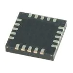
Ordering Information: See page 67. Pin Assignments Si4430/31/32
XOUT nSEL 15 SCLK 14 SDI 13 SDO 12 VDD_DIG 7 GPIO_0 8 GPIO_1 9 GPIO_2 10 11 NC VR_DIG nIRQ SDN XIN
Applications
Remote control Home security & alarm Telemetry Personal data logging Toy control Tire pressure monitoring Wireless PC peripherals
Remote meter reading Remote keyless entry Home automation Industrial control Sensor networks Health monitors Tag readers
VDD_RF 1 TX 2 RXp 3 RXn 4 NC 5 6 ANT
20 19 18 17 16
GND PAD
Description
Silicon Laboratories’ Si4430/31/32 devices are highly integrated, single chip wireless ISM transceivers. The high-performance EZRadioPRO® family includes a complete line of transmitters, receivers, and transceivers allowing the RF system designer to choose the optimal wireless part for their application. The Si4430/31/32’s high level of integration offers reduced BOM cost while simplifying the overall system design. The extremely low receive sensitivity (–121 dBm) coupled with industry leading +20 dBm output power ensures extended range and improved link performance. Built-in antenna diversity and support for frequency hopping can be used to further extend range and enhance performance. The Si4430/31/32 offers advanced radio features including continuous frequency coverage from 240–960 MHz in 156 Hz or 312 Hz steps allowing precise tuning control. Additional system features such as an automatic wake-up timer, low battery detector, 64 byte TX/RX FIFOs, automatic packet handling, and preamble detection reduce overall current consumption and allow the use of lower-cost system MCUs. An integrated temperature sensor, general purpose ADC, poweron-reset (POR), and GPIOs further reduce overall system cost and size. The Si4430/31/32’s digital receive architecture features a high-performance ADC and DSP based modem which performs demodulation, filtering, and packet handling for increased flexibility and performance. The direct digital transmit modulation and automatic PA power ramping ensure precise transmit modulation and reduced spectral spreading ensuring compliance with global regulations including FCC, ETSI, ARIB, and 802.15.4d regulations. An easy-to-use calculator is provided to quickly configure the radio settings, simplifying customer's system design and reducing time to market. Rev 1.1 10/10 Copyright © 2010 by Silicon Laboratories
Patents pending
Si4430/31/32
�S i4430/31/32-B1
Functional Block Diagram
2
Rev 1.1
�S i4430/31/32-B1 TABLE O F C ONTENTS
Section Page
1. Electrical Specifications . . . . . . . . . . . . . . . . . . . . . . . . . . . . . . . . . . . . . . . . . . . . . . . . . . .7 1.1. Definition of Test Conditions . . . . . . . . . . . . . . . . . . . . . . . . . . . . . . . . . . . . . . . . . . . 14 2. Functional Description . . . . . . . . . . . . . . . . . . . . . . . . . . . . . . . . . . . . . . . . . . . . . . . . . . . 15 2.1. Operating Modes . . . . . . . . . . . . . . . . . . . . . . . . . . . . . . . . . . . . . . . . . . . . . . . . . . . . 17 3. Controller Interface . . . . . . . . . . . . . . . . . . . . . . . . . . . . . . . . . . . . . . . . . . . . . . . . . . . . . . 18 3.1. Serial Peripheral Interface (SPI) . . . . . . . . . . . . . . . . . . . . . . . . . . . . . . . . . . . . . . . . 18 3.2. Operating Mode Control . . . . . . . . . . . . . . . . . . . . . . . . . . . . . . . . . . . . . . . . . . . . . . 20 3.3. Interrupts . . . . . . . . . . . . . . . . . . . . . . . . . . . . . . . . . . . . . . . . . . . . . . . . . . . . . . . . . 23 3.4. System Timing . . . . . . . . . . . . . . . . . . . . . . . . . . . . . . . . . . . . . . . . . . . . . . . . . . . . . 24 3.5. Frequency Control . . . . . . . . . . . . . . . . . . . . . . . . . . . . . . . . . . . . . . . . . . . . . . . . . . . 25 4. Modulation Options . . . . . . . . . . . . . . . . . . . . . . . . . . . . . . . . . . . . . . . . . . . . . . . . . . . . . . 32 4.1. Modulation Type . . . . . . . . . . . . . . . . . . . . . . . . . . . . . . . . . . . . . . . . . . . . . . . . . . . .32 4.2. Modulation Data Source . . . . . . . . . . . . . . . . . . . . . . . . . . . . . . . . . . . . . . . . . . . . . . 33 5. Internal Functional Blocks . . . . . . . . . . . . . . . . . . . . . . . . . . . . . . . . . . . . . . . . . . . . . . . . 37 5.1. RX LNA . . . . . . . . . . . . . . . . . . . . . . . . . . . . . . . . . . . . . . . . . . . . . . . . . . . . . . . . . . . 37 5.2. RX I-Q Mixer . . . . . . . . . . . . . . . . . . . . . . . . . . . . . . . . . . . . . . . . . . . . . . . . . . . . . . .37 5.3. Programmable Gain Amplifier . . . . . . . . . . . . . . . . . . . . . . . . . . . . . . . . . . . . . . . . . .37 5.4. ADC . . . . . . . . . . . . . . . . . . . . . . . . . . . . . . . . . . . . . . . . . . . . . . . . . . . . . . . . . . . . . . 37 5.5. Digital Modem . . . . . . . . . . . . . . . . . . . . . . . . . . . . . . . . . . . . . . . . . . . . . . . . . . . . . . 37 5.6. Synthesizer . . . . . . . . . . . . . . . . . . . . . . . . . . . . . . . . . . . . . . . . . . . . . . . . . . . . . . . .38 5.7. Power Amplifier . . . . . . . . . . . . . . . . . . . . . . . . . . . . . . . . . . . . . . . . . . . . . . . . . . . . . 39 5.8. Crystal Oscillator . . . . . . . . . . . . . . . . . . . . . . . . . . . . . . . . . . . . . . . . . . . . . . . . . . . . 40 5.9. Regulators . . . . . . . . . . . . . . . . . . . . . . . . . . . . . . . . . . . . . . . . . . . . . . . . . . . . . . . . . 40 6. Data Handling and Packet Handler . . . . . . . . . . . . . . . . . . . . . . . . . . . . . . . . . . . . . . . . . .41 6.1. RX and TX FIFOs . . . . . . . . . . . . . . . . . . . . . . . . . . . . . . . . . . . . . . . . . . . . . . . . . . . 41 6.2. Packet Configuration . . . . . . . . . . . . . . . . . . . . . . . . . . . . . . . . . . . . . . . . . . . . . . . . .42 6.3. Packet Handler TX Mode . . . . . . . . . . . . . . . . . . . . . . . . . . . . . . . . . . . . . . . . . . . . .43 6.4. Packet Handler RX Mode . . . . . . . . . . . . . . . . . . . . . . . . . . . . . . . . . . . . . . . . . . . . .43 6.5. Data Whitening, Manchester Encoding, and CRC . . . . . . . . . . . . . . . . . . . . . . . . . . 46 6.6. Preamble Detector . . . . . . . . . . . . . . . . . . . . . . . . . . . . . . . . . . . . . . . . . . . . . . . . . . 46 6.7. Preamble Length . . . . . . . . . . . . . . . . . . . . . . . . . . . . . . . . . . . . . . . . . . . . . . . . . . . . 47 6.8. Invalid Preamble Detector . . . . . . . . . . . . . . . . . . . . . . . . . . . . . . . . . . . . . . . . . . . . . 47 6.9. Synchronization Word Configuration . . . . . . . . . . . . . . . . . . . . . . . . . . . . . . . . . . . . . 47 6.10. Receive Header Check . . . . . . . . . . . . . . . . . . . . . . . . . . . . . . . . . . . . . . . . . . . . . . 48 6.11. TX Retransmission and Auto TX . . . . . . . . . . . . . . . . . . . . . . . . . . . . . . . . . . . . . . . 48 7. RX Modem Configuration . . . . . . . . . . . . . . . . . . . . . . . . . . . . . . . . . . . . . . . . . . . . . . . . . 49 7.1. Modem Settings for FSK and GFSK . . . . . . . . . . . . . . . . . . . . . . . . . . . . . . . . . . . . . 49 8. Auxiliary Functions . . . . . . . . . . . . . . . . . . . . . . . . . . . . . . . . . . . . . . . . . . . . . . . . . . . . . . 50 8.1. Smart Reset . . . . . . . . . . . . . . . . . . . . . . . . . . . . . . . . . . . . . . . . . . . . . . . . . . . . . . .50
Rev 1.1
3
�S i4430/31/32-B1
8.2. Microcontroller Clock . . . . . . . . . . . . . . . . . . . . . . . . . . . . . . . . . . . . . . . . . . . . . . . . .51 8.3. General Purpose ADC . . . . . . . . . . . . . . . . . . . . . . . . . . . . . . . . . . . . . . . . . . . . . . . 52 8.4. Temperature Sensor . . . . . . . . . . . . . . . . . . . . . . . . . . . . . . . . . . . . . . . . . . . . . . . . .53 8.5. Low Battery Detector . . . . . . . . . . . . . . . . . . . . . . . . . . . . . . . . . . . . . . . . . . . . . . . . .55 8.6. Wake-Up Timer and 32 kHz Clock Source . . . . . . . . . . . . . . . . . . . . . . . . . . . . . . . . 56 8.7. Low Duty Cycle Mode . . . . . . . . . . . . . . . . . . . . . . . . . . . . . . . . . . . . . . . . . . . . . . . . 58 8.8. GPIO Configuration . . . . . . . . . . . . . . . . . . . . . . . . . . . . . . . . . . . . . . . . . . . . . . . . . . 59 8.9. Antenna Diversity . . . . . . . . . . . . . . . . . . . . . . . . . . . . . . . . . . . . . . . . . . . . . . . . . . . 60 8.10. RSSI and Clear Channel Assessment . . . . . . . . . . . . . . . . . . . . . . . . . . . . . . . . . . 61 9. Reference Design . . . . . . . . . . . . . . . . . . . . . . . . . . . . . . . . . . . . . . . . . . . . . . . . . . . . . . . .62 10. Application Notes and Reference Designs . . . . . . . . . . . . . . . . . . . . . . . . . . . . . . . . . . 63 11. Customer Support . . . . . . . . . . . . . . . . . . . . . . . . . . . . . . . . . . . . . . . . . . . . . . . . . . . . . . 63 12. Register Table and Descriptions . . . . . . . . . . . . . . . . . . . . . . . . . . . . . . . . . . . . . . . . . . 64 13. Pin Descriptions: Si4430/31/32 . . . . . . . . . . . . . . . . . . . . . . . . . . . . . . . . . . . . . . . . . . . . 66 14. Ordering Information . . . . . . . . . . . . . . . . . . . . . . . . . . . . . . . . . . . . . . . . . . . . . . . . . . . . 67 15. Package Markings (Top Marks) . . . . . . . . . . . . . . . . . . . . . . . . . . . . . . . . . . . . . . . . . . . . 68 15.1. Si4430/31/32 Top Mark . . . . . . . . . . . . . . . . . . . . . . . . . . . . . . . . . . . . . . . . . . . . . . 68 15.2. Top Mark Explanation . . . . . . . . . . . . . . . . . . . . . . . . . . . . . . . . . . . . . . . . . . . . . . . 68 16. Package Outline: Si4430/31/32 . . . . . . . . . . . . . . . . . . . . . . . . . . . . . . . . . . . . . . . . . . . . 69 17. PCB Land Pattern: Si4430/31/32 . . . . . . . . . . . . . . . . . . . . . . . . . . . . . . . . . . . . . . . . . . . 70 Document Change List . . . . . . . . . . . . . . . . . . . . . . . . . . . . . . . . . . . . . . . . . . . . . . . . . . . . .72 Contact Information . . . . . . . . . . . . . . . . . . . . . . . . . . . . . . . . . . . . . . . . . . . . . . . . . . . . . . . .74
4
Rev 1.1
�S i4430/31/32-B1 L I S T O F F IGURES
Figure 1. Si4430/31 RX/TX Direct-Tie Application Example ..................................................... 16 Figure 2. Si4432 Antenna Diversity Application Example ......................................................... 16 Figure 3. SPI Timing.................................................................................................................. 18 Figure 4. SPI Timing—READ Mode ..........................................................................................19 Figure 5. SPI Timing—Burst Write Mode .................................................................................. 19 Figure 6. SPI Timing—Burst Read Mode .................................................................................. 19 Figure 7. State Machine Diagram.............................................................................................. 20 Figure 8. TX Timing................................................................................................................... 24 Figure 9. RX Timing .................................................................................................................. 24 Figure 10. Frequency Deviation ................................................................................................ 28 Figure 11. Sensitivity at 1% PER vs. Carrier Frequency Offset ................................................29 Figure 12. FSK vs GFSK Spectrums......................................................................................... 32 Figure 13. Direct Synchronous Mode Example......................................................................... 35 Figure 14. Direct Asynchronous Mode Example ....................................................................... 35 Figure 15. Microcontroller Connections..................................................................................... 36 Figure 16. PLL Synthesizer Block Diagram............................................................................... 38 Figure 17. FIFO Thresholds ...................................................................................................... 41 Figure 18. Packet Structure....................................................................................................... 42 Figure 19. Multiple Packets in TX Packet Handler .................................................................... 43 Figure 20. Required RX Packet Structure with Packet Handler Disabled ................................. 43 Figure 21. Multiple Packets in RX Packet Handler.................................................................... 43 Figure 22. Multiple Packets in RX with CRC or Header Error ................................................... 44 Figure 23. Operation of Data Whitening, Manchester Encoding, and CRC .............................. 46 Figure 24. Manchester Coding Example ...................................................................................46 Figure 25. Header ..................................................................................................................... 48 Figure 26. POR Glitch Parameters............................................................................................ 50 Figure 27. General Purpose ADC Architecture ......................................................................... 52 Figure 28. Temperature Ranges using ADC8 ........................................................................... 54 Figure 29. WUT Interrupt and WUT Operation.......................................................................... 57 Figure 30. Low Duty Cycle Mode .............................................................................................. 58 Figure 31. RSSI Value vs. Input Power..................................................................................... 61 Figure 32. TX/RX Direct-Tie Reference Design—Schematic.................................................... 62 Figure 33. 20-Pin Quad Flat No-Lead (QFN) ............................................................................69 Figure 34. PCB Land Pattern .................................................................................................... 70
Rev 1.1
5
�S i4430/31/32-B1 L I S T O F TABLES
Table 1. DC Characteristics1 ......................................................................................................7 Table 2. Synthesizer AC Electrical Characteristics1 ...................................................................8 Table 3. Receiver AC Electrical Characteristics1 .......................................................................9 Table 4. Transmitter AC Electrical Characteristics1 ................................................................. 10 Table 5. Auxiliary Block Specifications1 ...................................................................................11 Table 6. Digital IO Specifications (SDO, SDI, SCLK, nSEL, and nIRQ) ................................... 12 Table 7. GPIO Specifications (GPIO_0, GPIO_1, and GPIO_2) .............................................. 12 Table 8. Absolute Maximum Ratings ........................................................................................ 13 Table 9. Operating Modes ........................................................................................................17 Table 10. Serial Interface Timing Parameters .......................................................................... 18 Table 11. Operating Modes Response Time ............................................................................20 Table 12. Frequency Band Selection ....................................................................................... 26 Table 13. Packet Handler Registers ......................................................................................... 45 Table 14. Minimum Receiver Settling Time .............................................................................. 47 Table 15. POR Parameters ...................................................................................................... 50 Table 16. Temperature Sensor Range ..................................................................................... 53 Table 17. Antenna Diversity Control ......................................................................................... 60 Table 18. Register Descriptions ............................................................................................... 64 Table 19. Package Dimensions ................................................................................................ 69 Table 20. PCB Land Pattern Dimensions ................................................................................. 71
Rev 1.1
6
�S i4430/31/32-B1
1. Electrical Specifications
Table 1. DC Characteristics1
Parameter
Supply Voltage Range Power Saving Modes
Symbol
VDD IShutdown IStandby ISleep ISensor-LBD ISensor-TS IReady
Conditions
Min
1.8
Typ
3.0 15 450 1 1 1 800 8.5 18.5 85
Max
3.6 50 800 — — — — — — —
Units
V nA nA µA µA µA µA mA mA mA
RC Oscillator, Main Digital Regulator, and Low Power Digital Regulator OFF2 Low Power Digital Regulator ON (Register values retained) and Main Digital Regulator, and RC Oscillator OFF RC Oscillator and Low Power Digital Regulator ON (Register values retained) and Main Digital Regulator OFF Main Digital Regulator and Low Battery Detector ON, Crystal Oscillator and all other blocks OFF2 Main Digital Regulator and Temperature Sensor ON, Crystal Oscillator and all other blocks OFF2 Crystal Oscillator and Main Digital Regulator ON, all other blocks OFF. Crystal Oscillator buffer disabled Synthesizer and regulators enabled
— — — — — — — —
TUNE Mode Current RX Mode Current TX Mode Current —Si4432 TX Mode Current —Si4430/31
ITune IRX ITX_+20
txpow[2:0] = 111 (+20 dBm) Using Silicon Labs’ Reference Design. TX current consumption is dependent on match and board layout. txpow[2:0] = 110 (+13 dBm) Using Silicon Labs’ Reference Design. TX current consumption is dependent on match and board layout. txpow[2:0] = 010 (+1 dBm) Using Silicon Labs’ Reference Design. TX current consumption is dependent on match and board layout.
—
ITX_+13
—
30
—
mA
ITX_+1
—
17
—
mA
Notes: 1. All specification guaranteed by production test unless otherwise noted. Production test conditions and max limits are listed in the "Production Test Conditions" section on page 14. 2. Guaranteed by qualification. Qualification test conditions are listed in the "Production Test Conditions" section on page 14.
Rev 1.1
7
�S i4430/31/32-B1
Table 2. Synthesizer AC Electrical Characteristics1
Parameter Synthesizer Frequency Range—Si4431/32 Synthesizer Frequency Range—Si4430 Synthesizer Frequency Resolution2 Reference Frequency Input Level2 Synthesizer Settling Time2 Symbol FSYN FSYN FRES-LB FRES-HB fREF_LV Low Band, 240–480 MHz High Band, 480–960 MHz When using external reference signal driving XOUT pin, instead of using crystal. Measured peak-to-peak (VPP) Measured from exiting Ready mode with XOSC running to any frequency. Including VCO Calibration. Integrated over 250 kHz bandwidth (500 Hz lower bound of integration) F = 10 kHz F = 100 kHz F = 1 MHz F = 10 MHz Conditions Min 240 900 — — 0.7 Typ — — 156.25 312.5 — Max 930 960 — — 1.6 Units MHz MHz Hz Hz V
tLOCK
—
200
—
µs
Residual FM2 Phase Noise2
FRMS L(fM)
— — — — —
2 –80 –90 –115 –130
4 — — — —
kHzRMS dBc/Hz dBc/Hz dBc/Hz dBc/Hz
Notes: 1. All specification guaranteed by production test unless otherwise noted. Production test conditions and max limits are listed in the "Production Test Conditions" section on page 14. 2. Guaranteed by qualification. Qualification test conditions are listed in the "Production Test Conditions" section on page 14.
8
Rev 1.1
�S i4430/31/32-B1
Table 3. Receiver AC Electrical Characteristics1
Parameter RX Frequency Range—Si4431/32 RX Frequency Range—Si4430 RX Sensitivity2 Symbol FRX FRX PRX_2 PRX_40 PRX_100 PRX_125 PRX_OOK (BER < 0.1%) (2 kbps, GFSK, BT = 0.5, f = 5 kHz)3 (BER < 0.1%) (40 kbps, GFSK, BT = 0.5, f = 20 kHz)3 (BER < 0.1%) (100 kbps, GFSK, BT = 0.5, f = 50 kHz)3 (BER < 0.1%) (125 kbps, GFSK, BT = 0.5, f = 62.5 kHz) (BER < 0.1%) (4.8 kbps, 350 kHz BW, OOK)3 (BER < 0.1%) (40 kbps, 400 kHz BW, OOK)3 Up to +5 dBm Input Level 915 MHz 868 MHz 433 MHz 315 MHz Conditions Min 240 900 — Typ — — –121 Max 930 960 — Units MHz MHz dBm
—
–108
—
dBm
—
–104
—
dBm
—
–101
—
dBm
— — 2.6 — — — — — — — — — — — — — —
–110 –102 — 0 51–60j 54–63j 89–110j 107–137j ±0.5 –31 –35 –40 –52 –56 –63 –30 —
— — 620 0.1 — — — — — — — — — — — — –54
dBm dBm kHz ppm
RX Channel Bandwidth3 BER Variation vs Power Level3 LNA Input Impedance3 (Unmatched—measured differentially across RX input pins) RSSI Resolution 1-Ch Offset Selectivity
3 3
BW PRX_RES RIN-RX
RESRSSI C/I1-CH
dB dB dB dB dB dB dB dB dBm
Desired Ref Signal 3 dB above sensitivity, BER < 0.1%. Interferer and desired modu2-Ch Offset Selectivity C/I2-CH lated with 40 kbps F = 20 kHz GFSK with 3 3-Ch Offset Selectivity C/I3-CH BT = 0.5, channel spacing = 150 kHz Blocking at 1 MHz Offset3 1MBLOCK Desired Ref Signal 3 dB above sensitivity. Interferer and desired modulated with Blocking at 4 MHz Offset3 4MBLOCK 40 kbps F = 20 kHz GFSK with BT = 0.5 Blocking at 8 MHz Offset3 8MBLOCK Image Rejection3 ImREJ POB_RX1 Rejection at the image frequency. IF=937 kHz Measured at RX pins
Spurious Emissions3
Notes: 1. All specification guaranteed by production test unless otherwise noted. Production test conditions and max limits are listed in the "Production Test Conditions" section on page 14. 2. Receive sensitivity at multiples of 30 MHz may be degraded. If channels with a multiple of 30 MHz are required it is recommended to shift the crystal frequency. Contact Silicon Labs Applications Support for recommendations. 3. Guaranteed by qualification. Qualification test conditions are listed in the "Production Test Conditions" section on page 14.
Rev 1.1
9
�S i4430/31/32-B1
Table 4. Transmitter AC Electrical Characteristics1
Parameter TX Frequency Range—Si4431/32 TX Frequency Range—Si4430 FSK Data Rate2 OOK Data Rate
2
Symbol FTX FTX DRFSK DROOK Δf1 Δf2 ΔfRES PTX PTX PRF_OUT PRF_TEMP PRF_FREQ B*T POB-TX1 POB-TX2
Conditions
Min 240 900 0.123 0.123
Typ — — — —
Max 930 960 256 40 ±320 ±160
Units MHz MHz kbps kbps kHz kHz kHz dBm dBm dB dB dB
Modulation Deviation Modulation Deviation Resolution2 Output Power Range—Si44323 Output Power Range—Si4430/313 TX RF Output Steps2 TX RF Output Variation vs. Temperature TX RF Output Level Variation vs. Frequency2 Transmit Modulation Filtering2 Spurious Emissions2 Level2
860–960 MHz 240–860 MHz
±0.625 ±0.625 — +1 –8 0.625 — — 3 2 1 0.5 — — — —
— +20 +13 — — — — –54 –54 –42 –42
controlled by txpow[2:0] –40 to +85 C Measured across any one frequency band Gaussian Filtering Bandwith Time Product POUT = +13 dBm, Frequencies