Si50122-A5/A6
C R YS TA L - L ESS P C I -E X P R E S S G EN 1 , G EN 2, & G EN 3
DUAL O UTPUT C LOCK G ENERATOR
Features
Crystal-less clock generator with
integrated CMEMS
PCI-Express Gen 1/2/3 compliant
Two PCIe 100 MHz differential
HCSL outputs
One 25 MHz single-ended
LVCMOS output
Supports Serial (ATA) at
100 MHz
Low power differential output
buffers
No termination resistors required
for differential output clocks
Triangular spread spectrum
profile for maximum EMI
reduction (Si50122-A6)
Industrial Temperature –40 to
85 °C
2.5 V, 3.3 V Power supply
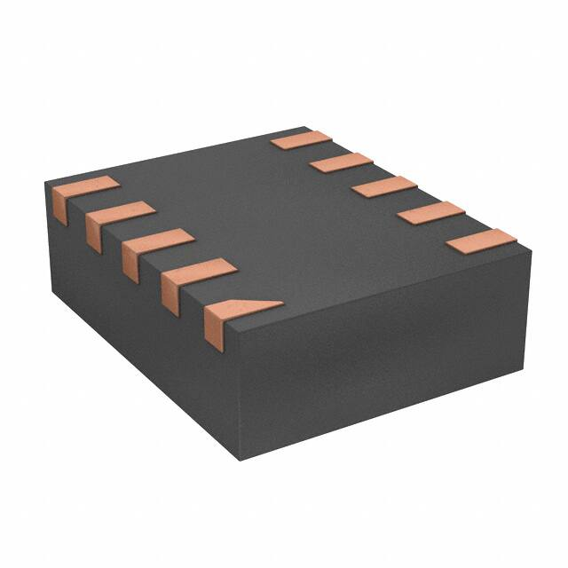
Small package 10-pin TDFN
(2.0x2.5 mm)
Si50122-A5 does not support
spread spectrum outputs
Si50122-A6 supports 0.5% down
spread outputs
Ordering Information:
See page 10
Pin Assignments
Applications
Network Attached Storage
Multi-function Printer
Digital TV
Set top box
Solid State Drives (SSD)
Wireless Access Point
Home Gateway
Digital Video Cameras
VSS
REFOUT
Description
Si50122-A5/A6 is a high performance, crystal-less PCIe clock generator
that can generate two 100 MHz PCIe clock and one 25 MHz LVCMOS
clock outputs. The clock outputs are compliant to PCIe Gen 1, Gen 2, and
Gen 3 specifications. The ultra-small footprint (2.0x2.5 mm) and industryleading low power consumption make Si50122-A5/A6 the ideal clock
solution for consumer and embedded applications where board space is
limited and low power is needed.
1
10
VDD
2
9
VDD
8
D IF F2
Si50122
NC
3
D IF F1
4
7
D IFF2
D IF F1
5
6
VSS
Patents pending
Functional Block Diagram
VDD
REFOUT
DIFF1
CMEMS
PLL
(SSC)
Divider
DIFF2
VSS
Rev 0.7 9/14
Copyright © 2014 by Silicon Laboratories
Si50122-A5/A6
�Si50122-A5/A6
2
Rev 0.7
�Si50122-A5/A6
TABLE O F C ONTENTS
Section
Page
1. Electrical Specifications . . . . . . . . . . . . . . . . . . . . . . . . . . . . . . . . . . . . . . . . . . . . . . . . . . .4
2. Test and Measurement Setup . . . . . . . . . . . . . . . . . . . . . . . . . . . . . . . . . . . . . . . . . . . . . . .7
3. Pin Descriptions . . . . . . . . . . . . . . . . . . . . . . . . . . . . . . . . . . . . . . . . . . . . . . . . . . . . . . . . . .9
4. Ordering Guide . . . . . . . . . . . . . . . . . . . . . . . . . . . . . . . . . . . . . . . . . . . . . . . . . . . . . . . . . . 10
5. Package Outlines . . . . . . . . . . . . . . . . . . . . . . . . . . . . . . . . . . . . . . . . . . . . . . . . . . . . . . . .11
6. Recommended Design Guideline . . . . . . . . . . . . . . . . . . . . . . . . . . . . . . . . . . . . . . . . . . . 13
Contact Information . . . . . . . . . . . . . . . . . . . . . . . . . . . . . . . . . . . . . . . . . . . . . . . . . . . . . . . .14
Rev 0.7
3
�Si50122-A5/A6
1. Electrical Specifications
Table 1. Recommended Operating Conditions
Parameter
Symbol
Test Condition
Min
Typ
Max
Unit
Supply Voltage (3.3 V Supply)
VDD
3.3 V ± 10%
2.97
3.3
3.63
V
Supply Voltage (2.5 V Supply)
VDD
2.5 V ± 10%
2.25
2.5
2.75
V
Table 2. DC Electrical Specifications
Parameter
Symbol
Test Condition
Min
Typ
Max
Unit
Operating VoltageVDD=3.3 V
VDD
3.3 V ± 10%
2.97
3.30
3.63
V
Operating VoltageVDD=2.5 V
VDD
2.5 V ± 10%
2.25
2.5
2.75
V
Operating Supply Current
IDD
Full active; 3.3 V ± 10%
—
20
23
mA
Full active; 2.5 V ± 10%
—
18
21
mA
CIN
Input Pin Capacitance
—
3
5
pF
COUT
Output Pin Capacitance
—
—
5
pF
Input Pin Capacitance
Output Pin Capacitance
4
Rev 0.7
�Si50122-A5/A6
Table 3. AC Electrical Specifications
Parameter
Symbol
Test Condition
Min
Typ
Max
Unit
TDC
Measured at 0 V differential
45
—
55
%
TSKEW
Measured at 0 V differential
—
—
100
ps
Output Frequency
FOUT
VDD = 3.3 V
—
100
—
MHz
Frequency Accuracy
FACC
All output clocks
—
—
100
ppm
Slew Rate
tr/f2
Measured differentially from
±150 mV
0.6
—
5.0
V/ns
Crossing Point Voltage at 0.7 V
Swing
VOX
300
—
550
mV
Voltage High
VHIGH
—
—
1.15
V
Voltage Low
VLOW
–0.3
—
—
V
Spread Range
SRNG
Down Spread, -A6 only
—
—
–0.5
%
Modulation Frequency
FMOD
-A6 only
30
31.5
33
kHz
DIFF Clocks
Duty Cycle
Skew
DIFF Clocks Jitter Parameters, VDD = 3.3 V ±10%
PCIe Gen1 Pk-Pk
Pk-PkGEN1
PCIe Gen 1
—
20.7
35
ps
PCIe Gen2 Phase Jitter
RMSGEN2
10 kHz < F < 1.5 MHz
—
0.8
2.1
ps
1.5 MHz < F < Nyquist
—
1.4
2.2
ps
Includes PLL BW 2-4 MHz,
CDR = 10 MHz
—
0.4
0.7
ps
PCIe Gen3 Phase Jitter
RMSGEN3
DIFF Clocks Jitter Parameters, VDD = 2.5 V ±10%
PCIe Gen1 Pk-Pk
Pk-PkGEN1
PCIe Gen 1
—
25
40
ps
PCIe Gen2 Phase Jitter
RMSGEN2
10 kHz < F < 1.5 MHz
—
0.9
2.9
ps
1.5 MHz < F < Nyquist
—
1.7
3.0
ps
RMSGEN3
Includes PLL BW 2-4 MHz,
CDR = 10 MHz
—
0.4
0.7
ps
TDC
Measurement at 1.5 V
45
—
55
%
Output Rise Time
tr
CL = 10 pF, 20% to 80%
1.2
3.0
ns
Output Fall Time
tf
CL = 10 pF, 20% to 80%
1.2
3.0
ns
Cycle to Cycle Jitter
TCCJ
Measurement at 1.5 V
—
—
250
ps
Long Term Accuracy
LACC
Measured at 1.5 V
—
—
50
ppm
TSTABLE
First power up to first output
—
—
10
ms
PCIe Gen3 Phase Jitter
25 MHz at 3.3 V
Duty Cycle
Powerup Time
Clock Stabilization from Powerup
Note: Visit www.pcisig.com for complete PCIe specifications.
Rev 0.7
5
�Si50122-A5/A6
Table 4. Thermal Conditions
Parameter
Symbol
Test Condition
Min
Temperature, Storage
TS
Non-functional
Temperature, Operating Ambient
TA
Temperature, Junction
Typ
Max
Unit
–65
150
°C
Functional
–40
85
°C
TJ
Functional
—
150
°C
Dissipation, Junction to Case
ØJC
JEDEC (JESD 51)
—
38.3
°C/W
Dissipation, Junction to Ambient
ØJA
JEDEC (JESD 51)
—
90.4
°C/W
Test Condition
Min
Max
Unit
—
4.6
V
Table 5. Absolute Maximum Conditions
Parameter
Main Supply Voltage
Input Voltage
ESD Protection (Human Body Model)
Flammability Rating
Symbol
VDD_3.3V
Typ
VIN
Relative to VSS
–0.5
4.6
VDC
ESDHBM
JEDEC (JESD 22 - A114)
2000
—
V
UL-94
UL (Class)
V–0
Note: While using multiple power supplies, the voltage on any input or I/O pin cannot exceed the power pin during powerup.
Power supply sequencing is NOT required.
6
Rev 0.7
�Si50122-A5/A6
2. Test and Measurement Setup
This diagram shows the test load configuration for the differential clock signals.
M e a s u re m e n t
P o in t
L1
O U T+
5 0
2 pF
L1 = 5"
M e a s u re m e n t
P o in t
L1
O U T-
5 0
2 pF
Figure 1. 0.7 V Differential Load Configuration
Figure 2. Differential Measurement for Differential Output Signals
(for AC Parameters Measurement)
Rev 0.7
7
�Si50122-A5/A6
Figure 3. Single-ended Measurement for Differential Output Signals
(for AC Parameters Measurement)
L1 = 0.5", L2 = 5"
50
REF
Measurement
Point
L1
33
L2
10 pF
Figure 4. Single-ended Clocks with Single Load Configuration
80%
1.5V
20%
Figure 5. Single-ended Output Signal (for AC Parameter Measurement)
8
Rev 0.7
�Si50122-A5/A6
3. Pin Descriptions
VSS
1
10
VDD
REFOUT
2
9
VDD
8
DIFF2
Si50122
NC
3
DIFF1
4
7
DIFF2
DIFF1
5
6
VSS
Figure 6. 10-Pin TDFN
Table 6. Si50122-Ax-GM 10-Pin TDFN Descriptions
Pin #
Name
Type
Description
1
VSS
GND
2
REFOUT
3
NC
4
DIFF1
O, DIF 0.7 V, 100 MHz differential clock
5
DIFF1
O, DIF 0.7 V, 100 MHz differential clock
6
VSS
7
DIFF2
O, DIF 0.7 V, 100 MHz differential clock
8
DIFF2
O, DIF 0.7 V, 100 MHz differential clock
9
VDD
PWR Power supply
10
VDD
PWR Power supply
Ground
O, SE 25 MHz LVCMOS clock
NC
GND
No Connect
Ground
Rev 0.7
9
�Si50122-A5/A6
4. Ordering Guide
Part Number
Spread Option
Package Type
Temperature
Si50122-A5-GM
No Spread
10-pin TDFN
Industrial, –40 to 85 C
Si50122-A5-GMR
No Spread
10-pin TDFN—Tape and Reel
Industrial, –40 to 85 C
Si50122-A6-GM
–0.5% Spread
10-pin TDFN
Industrial, –40 to 85 C
Si50122-A6-GMR
–0.5% Spread
10-pin TDFN—Tape and Reel
Industrial, –40 to 85 C
Si 50122
52112
Ax
Bx
Base part number
A : Product Revision A
x=5 : non
x=3
non- spread outputs
x=6
x=4 : -0.5 % spread outputs
GMR
GM2R
Operating Temp Range
:
G : - 40 to + 85 ° C
M
10 - TDFNPackage
Package,
ROHS6, Pb, Pb-free
free
M::10-TDFN
, ROHS6
R : Tape & Reel
( blank) = Tubes
Figure 7. Ordering Information
10
Rev 0.7
�Si50122-A5/A6
5. Package Outlines
Figure 8. 10-Pin TDFN Package Drawing
Rev 0.7
11
�Si50122-A5/A6
Table 7. Package Diagram Dimensions
Symbol
Min
Nom
Max
A
0.80
0.85
0.90
A1
0.00
—
0.05
A3
b
0.203 REF
0.20
0.25
D
2.00 BSC
e
0.50 BSC
E
2.50 BSC
L
0.35
0.4
aaa
0.10
bbb
0.10
ccc
0.10
ddd
0.05
eee
0.08
0.30
0.45
Notes:
1. All dimensions shown are in millimeters (mm) unless otherwise noted.
2. Dimensioning and Tolerancing per ANSI Y14.5M-1994.
12
Rev 0.7
�Si50122-A5/A6
6. Recommended Design Guideline
3.3 V / 2.5V
FB
VDD
4.7uF
0.1uF
Si 50122
Note: FB Specifications:
DC resistance 0.1–0.3
Impedance at 100 MHz > 1000
Figure 9. Recommended Application Schematic
Rev 0.7
13
�ClockBuilder Pro
One-click access to Timing tools,
documentation, software, source
code libraries & more. Available for
Windows and iOS (CBGo only).
www.silabs.com/CBPro
Timing Portfolio
www.silabs.com/timing
SW/HW
Quality
Support and Community
www.silabs.com/CBPro
www.silabs.com/quality
community.silabs.com
Disclaimer
Silicon Laboratories intends to provide customers with the latest, accurate, and in-depth documentation of all peripherals and modules available for system and software implementers
using or intending to use the Silicon Laboratories products. Characterization data, available modules and peripherals, memory sizes and memory addresses refer to each specific
device, and "Typical" parameters provided can and do vary in different applications. Application examples described herein are for illustrative purposes only. Silicon Laboratories
reserves the right to make changes without further notice and limitation to product information, specifications, and descriptions herein, and does not give warranties as to the accuracy
or completeness of the included information. Silicon Laboratories shall have no liability for the consequences of use of the information supplied herein. This document does not imply
or express copyright licenses granted hereunder to design or fabricate any integrated circuits. The products must not be used within any Life Support System without the specific
written consent of Silicon Laboratories. A "Life Support System" is any product or system intended to support or sustain life and/or health, which, if it fails, can be reasonably expected
to result in significant personal injury or death. Silicon Laboratories products are generally not intended for military applications. Silicon Laboratories products shall under no
circumstances be used in weapons of mass destruction including (but not limited to) nuclear, biological or chemical weapons, or missiles capable of delivering such weapons.
Trademark Information
Silicon Laboratories Inc., Silicon Laboratories, Silicon Labs, SiLabs and the Silicon Labs logo, CMEMS®, EFM, EFM32, EFR, Energy Micro, Energy Micro logo and combinations
thereof, "the world’s most energy friendly microcontrollers", Ember®, EZLink®, EZMac®, EZRadio®, EZRadioPRO®, DSPLL®, ISOmodem ®, Precision32®, ProSLIC®, SiPHY®,
USBXpress® and others are trademarks or registered trademarks of Silicon Laboratories Inc. ARM, CORTEX, Cortex-M3 and THUMB are trademarks or registered trademarks of
ARM Holdings. Keil is a registered trademark of ARM Limited. All other products or brand names mentioned herein are trademarks of their respective holders.
Silicon Laboratories Inc.
400 West Cesar Chavez
Austin, TX 78701
USA
http://www.silabs.com
�


 工商网监
湘ICP备2023018690号
工商网监
湘ICP备2023018690号
